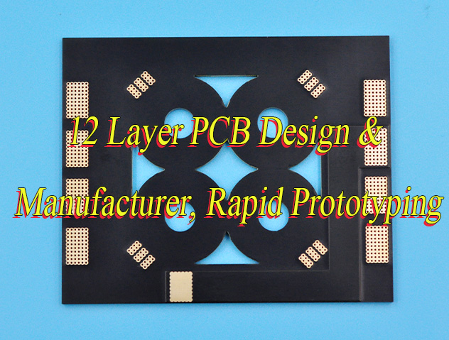
What is 12 Layer PCB fabrication? This guide details its applications, fabrication process, our specialized services, capabilities and how to get a quote.
Are you troubled with these problems?
- How to solve signal crosstalk and delay issues in dense 12-layer PCB routing?
- With multiple layers and challenging PCB material expansion control, how to ensure interlayer alignment accuracy?
- Can quality and efficiency be balanced given long prototype cycles and cost pressures?
As a 12 layer PCB fabrication manufacturer, EBest Circuit (Best Technology) can provide you service and solutions:
- Precise Stack-Up Design + Signal Integrity Simulation: Utilizing proprietary impedance calculation models and EMC simulation tools to preemptively mitigate high-frequency signal distortion risks, ensuring clean, interference-free critical signal paths.
- Smart Lamination Process + Laser Positioning System: Adopting TG170 high-stability substrates paired with real-time temperature-pressure monitoring and X-ray hole calibration, achieving ≤50μm layer misalignment tolerance to overcome high-layer alignment challenges.
- Flexible Production Line + Tiered Pricing Strategy: Establishing a rapid prototyping line for 5-7 day prototype delivery; implementing “step-down pricing” for small-to-medium batches to reduce upfront investment costs.
Welcome to contact us if you have any inquiry for multilayer PCB Board: sales@bestpcbs.com.
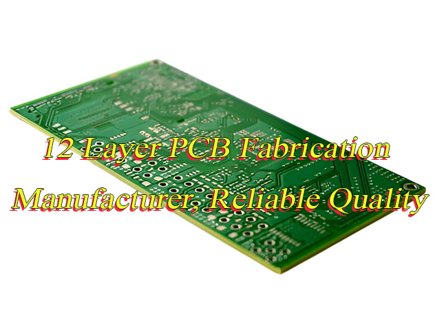
What Is 12 Layer PCB Fabrication?
12 layer PCB fabrication refers to the process of producing printed circuit boards with 12 layers of conductive copper foil circuit patterns. These layers (including signal layers, power layers, and ground layers) are interconnected through precision lamination and plated copper vias (PTH) to form complex, high-density circuit channels. This multilayer structure is designed for complex electronic devices that require extremely high performance, high-speed signal integrity, strict power distribution, and electromagnetic compatibility (EMC). The manufacturing process involves precise interlayer alignment, drilling, electroplating, and stringent control, making it significantly more technically challenging and costly than low-layer PCBs.
When to Use 12-Layer PCB Fabrication?
Applications of 12 layer PCB fabrication:
- Communication equipment: such as 5G base stations, high-speed routers, switches, and satellite communication equipment, requires processing high-frequency signals and ensuring signal integrity.
- High-performance computing: servers, data center equipment, and artificial intelligence hardware need to support multi-processor collaboration and high-speed data transmission.
- Medical electronics: CT scanners, monitoring equipment, and medical imaging systems require high reliability and interference immunity.
- Automotive electronics: Advanced Driver Assistance Systems (ADAS), in-vehicle infotainment, and engine control units need to meet stringent environmental stability standards.
- Industrial automation: industrial controllers, robotic systems, and precision instruments need to implement multi-channel signal control and power management.
- Aerospace and defense: avionics equipment, radar systems, and military communication hardware require resistance to extreme environments and long-term reliability.
12 Layer PCB Fabrication Process
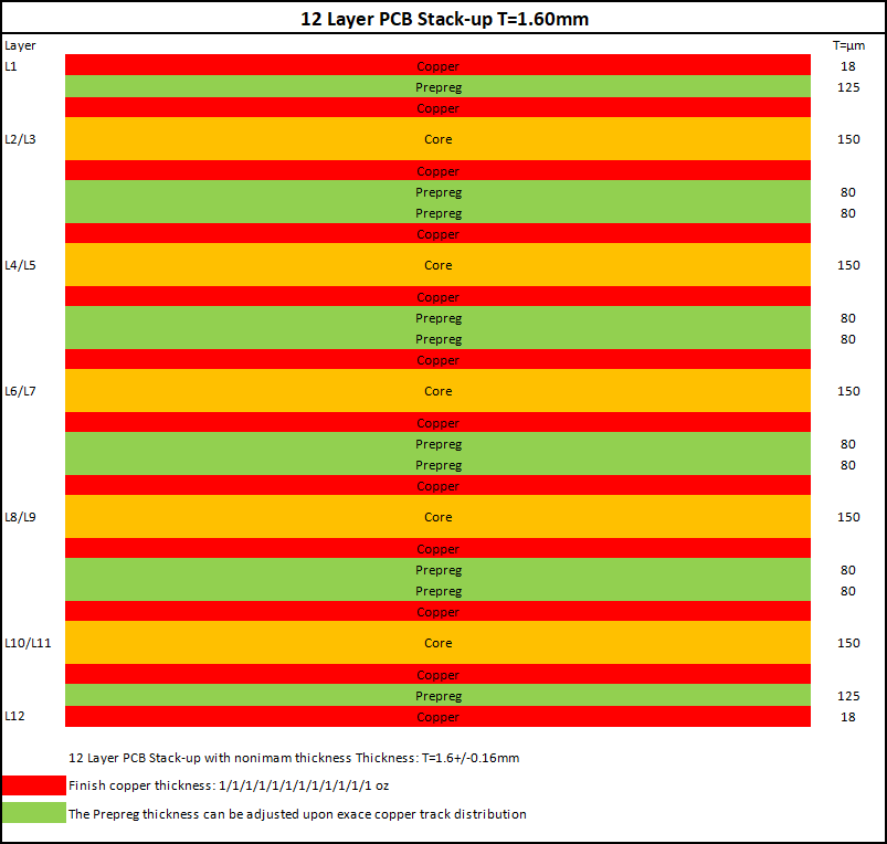
1. Stackup Design
- Signal-Power-Ground Coordination Design: Adhere to three principles: signal layers adjacent to ground layers, power layers partitioned and isolated, and impedance accurately matched. Typical 12-layer structures use “signal-ground-power-ground” repeating units. High-frequency signal layers (e.g., ≥25Gbps) should be sandwiched between two ground layers (stripline structure) with spacing ≤0.5mm to suppress crosstalk below -40dB. Power layers are partitioned by voltage domains (e.g., 3.3V/1.8V/0.9V) with ≥0.5mm ground isolation bands to reduce power ripple coupling by 50%.
- Layer Thickness Balance and Symmetry Control: Top/bottom layer base material thickness and copper foil weight must be strictly symmetric (e.g., 1oz copper + 0.2mm base for outer layers, 0.5oz copper + 0.15mm base for inner layers). Total thickness is controlled at 2.0±0.1mm with warpage ≤0.75% to avoid connector insertion issues or mechanical strength degradation.
- EMC Optimization Design: Minimize differential/common-mode radiation through “signal layer adjacent to reference planes” and “tight coupling between power and ground planes”. For example, a 12-layer board can allocate 6 signal layers and 6 reference planes, ensuring high-frequency signals reference the same plane during layer transitions to reduce cross-partition phenomena.
2. Inner Layer Core Board Production
- Pattern Transfer Precision Control: Utilize laser direct imaging (LDI) technology with exposure energy accuracy ±50mJ/cm² and line width/spacing accuracy ≤75μm. After cleaning, copper-clad laminates are coated with photosensitive film. UV light solidifies transparent regions, while unexposed areas are stripped using alkaline solutions (e.g., NaOH). Post-etching micro-etching enhances surface roughness to Ra 0.8-1.2μm for improved interlayer bonding.
- Black Oxide/Brown Oxide Treatment: Inner layer copper surfaces undergo chemical oxidation to form micro-porous structures (1-2μm thick), ensuring no delamination risk during lamination and enhancing adhesion for subsequent hole metallization.
3. Lamination Process
- Precision Temperature-Pressure Control: In vacuum environments, segmented pressure application is used: 5-15 minutes of pre-pressing to expel air bubbles, followed by 30-60 minutes of full-pressure curing at 180-220°C and 200-400psi pressure. Heating rates are controlled at 2-5°C/min to prevent thermal stress-induced delamination or warpage. Prepreg (PP) melts and flows during curing, forming the multilayer substrate with interlayer alignment accuracy ≤±50μm.
- Material Compatibility Verification: Base material CTE (coefficient of thermal expansion) must match adhesive properties. Cleanliness is maintained below Class 1000 with humidity at 40-60%RH to avoid moisture absorption affecting interlayer bonding.
4. Drilling and Hole Metallization
- High-Precision Drilling Technology: Mechanical drilling covers diameters of 0.1-0.3mm at speeds of 100-200kRPM, feed rates of 0.5-1.5mm/s, and coolant flows of 500-1000mL/min, achieving hole wall roughness ≤20μm. Laser drilling (CO₂/Nd:YAG) for blind/buried holes supports diameters as small as 50μm, requiring controlled carbon residue removal via plasma etching or chemical cleaning to ensure clean hole walls.
- Hole Metallization Quality Control: Chemical copper plating begins with a 1μm conductive layer, thickened to 25μm via electroplating with thickness uniformity ≤±10%. Reliability is validated through thermal shock tests (-40°C to 125°C for 1000 cycles) to prevent copper layer peeling or fracture.
5. Outer Layer Circuit Production
- Pattern Transfer and Etching: Positive film processes transfer outer layer circuits. Exposure energy ranges from 600-800mJ/cm², developer concentration is 1.2%, and development time is 60-90 seconds for precise window dimensions (e.g., 0.1mm window deviation ≤±0.02mm). Post-etching tin stripping preserves copper traces with line width/spacing accuracy ±5%.
- Solder Mask Application: Screen printing (300-400 mesh) or spraying (atomization pressure 0.3-0.5MPa) applies solder mask with wet film thickness 30-40μm, reducing to 20-30μm after drying. Pre-baking at 70-80°C removes solvents, exposure defines windows at 500-800mJ/cm², and post-curing at 120-150°C enhances adhesion to 7N/cm with insulation resistance ≥10¹³Ω.
6. Surface Treatment
- Process Comparison and Selection: Hot air solder leveling (HAL) offers low cost but higher surface roughness; OSP is simple but has a storage life ≤3 months. Electroless nickel/immersion gold (ENIG) suits fine-pitch leads with excellent durability; immersion silver/tin suits high-frequency applications but requires moisture and electronic migration protection.
7. Electrical Testing and Reliability Verification
- Full-Link Testing Standards: Flying probe tests detect opens/shorts with impedance accuracy ±10%; fixture tests validate functional connectivity. Reliability tests include thermal shock (-40°C to 125°C for 500 cycles), thermal cycling (-55°C to 125°C for 1000 cycles), humid heat aging (85°C/85%RH for 168 hours), and vibration tests (random vibration 20G). Hole pull strength ≥10N and peel strength ≥1.0N/mm are ensured.
- Non-Destructive Testing Techniques: X-ray inspection checks hole metal filling rates; SEM observes microstructural defects; insulation resistance ≥10¹¹Ω and voltage withstand tests validate electrical isolation.
8. Final Inspection and Packaging
- Comprehensive Quality Inspection: Visual checks assess pad integrity and solder mask defects (e.g., bubbles/pinholes); dimensional measurements maintain ±0.1mm accuracy. Packaging uses anti-static bags + corrugated boxes with moisture/vibration protection, compliant with IPC-A-600 standards for damage-free transport.
- Environmental Sustainability: Wastewater undergoes “physical-chemical + biochemical + membrane filtration” tertiary treatment with reuse rate ≥70%. Exhaust gases are purified via spray towers/catalytic combustion to emissions <10mg/m³. Hazardous waste is entrusted to licensed recyclers with copper recovery ≥95%, achieving green production and cost efficiency.
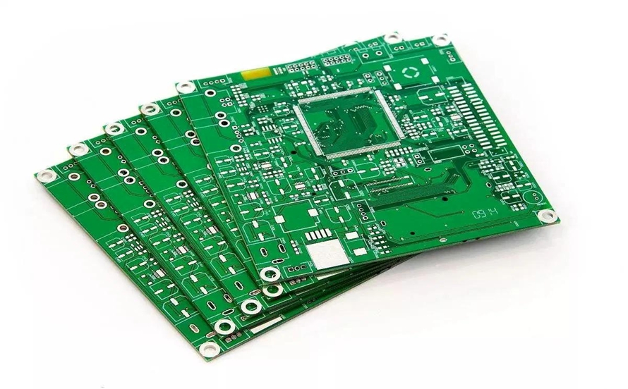
12 Layer PCB Board Fabrication Services We Offered
- High Reliability Material Guarantee: Utilizes Grade A FR-4 substrate and high-Tg laminate, certified by ISO 9001 quality system, ensuring electrical stability across -40°C to 125°C wide temperature range and reducing after-sales failure costs caused by material defects.
- Rapid Prototyping Service: Offers 24-hour quick-turn prototyping with DFM design verification to identify manufacturability issues at the prototype stage, accelerating time-to-market by over 30% and aiding in seizing market opportunities.
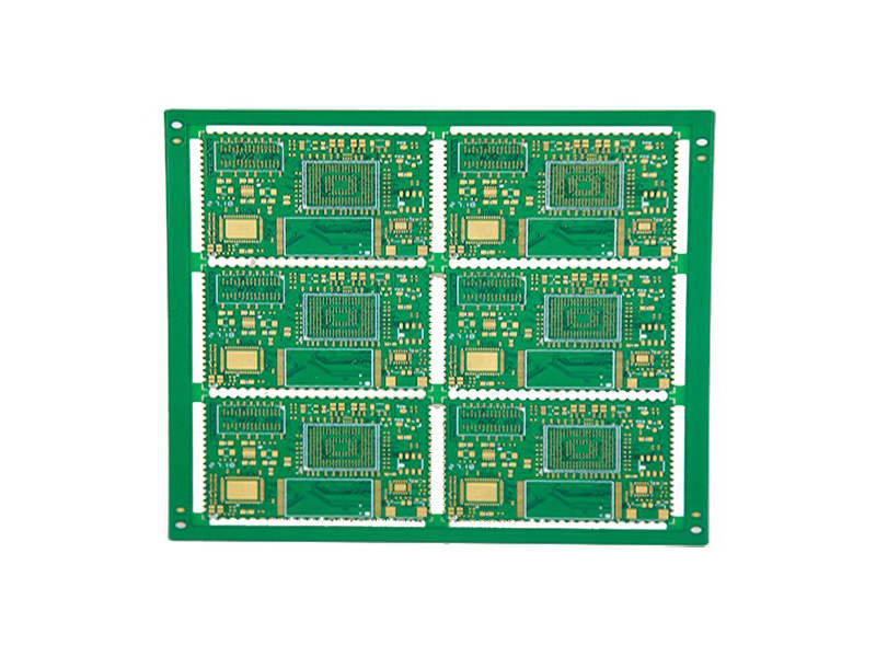
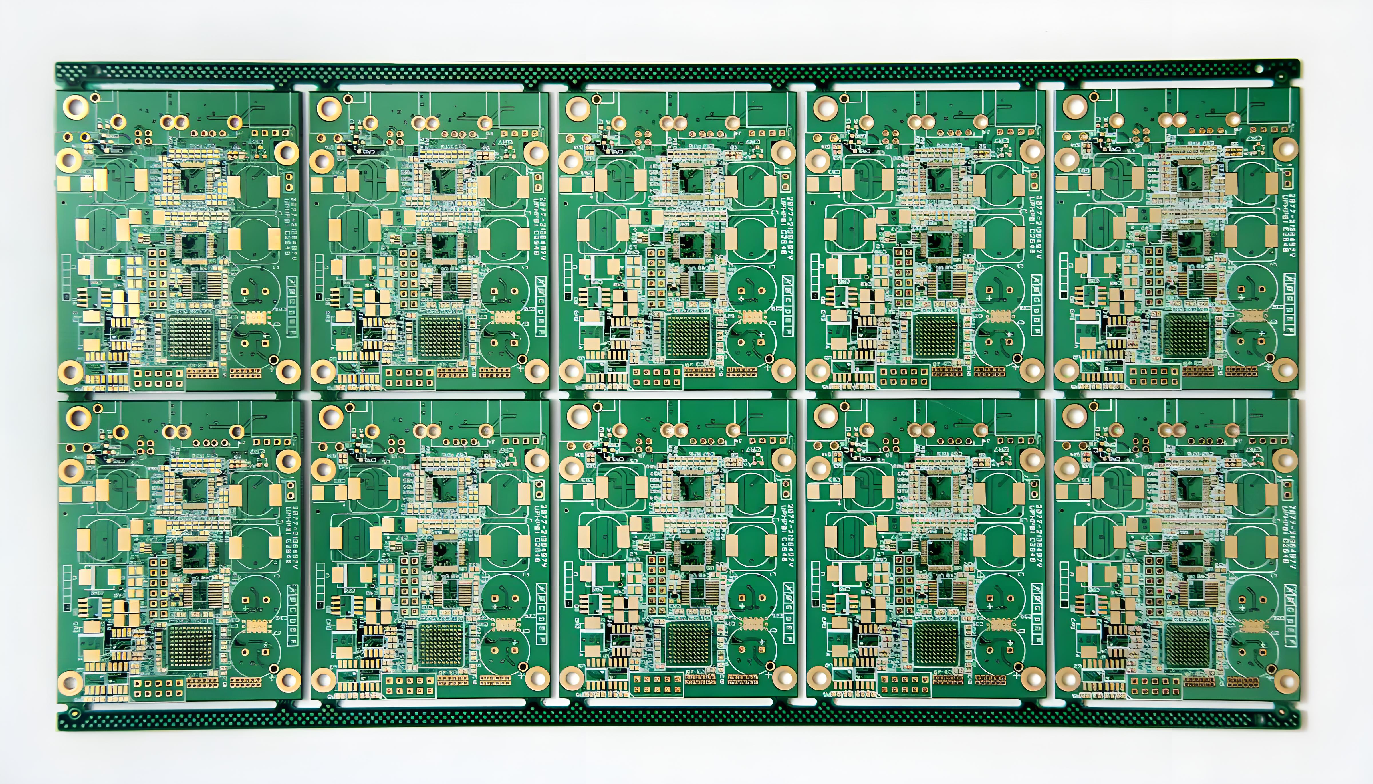
- Cost Optimization Solution: Reduces per-board cost by 15%-20% through intelligent panelization algorithms and material utilization optimization, while providing tiered pricing to accommodate cost-sensitive needs across different order volumes.
- Professional Design Support: Provides free DFM analysis conducted by senior engineers for signal integrity simulation, thermal design optimization, and manufacturability review, proactively avoiding design flaws and reducing R&D iterations.
- Flexible Capacity Scaling: Equipped with 5 fully automated production lines supporting seamless transition from small-batch trials (50+ pieces) to mass production (100,000+ m² monthly capacity) for project scalability.
- 24/7 Technical Support: Features bilingual technical teams offering end-to-end support from design consultation to post-sales troubleshooting, with ≤2-hour response time for uninterrupted project progress.
- Customized Packaging & Logistics: Implements ESD-safe and vacuum packaging tailored to product specifications, integrated with global logistics networks for secure delivery and minimized transport damage risks.
Why Choose EBest Circuit (Best Technology) as 12 Layer PCB Fabrication Manufacturer?
Reasons why choose us as 12 Layer PCB fabrication manufacturer:
- Quality Compliance with Global Certifications: Certified to ISO 9001:2015, IATF 16949:2016, ISO 13485:2016, RoHS, and REACH, ensuring full compliance with automotive, medical, and consumer electronics standards. This guarantees seamless market access for clients worldwide.
- Strict Quality Control: Implements AOI , X-Ray and manual verification for 100% testing of critical parameters like layer alignment, impedance control, and hole copper thickness. Defect rates are below 0.03%, exceeding industry benchmarks for reliability.
- Transparent Pricing with No Hidden Costs: Modular pricing structure clearly breaks down engineering, material, and testing fees. Customizable cost optimization schemes reduce total expenses by 15-20% compared to competitors, enhancing client competitiveness.
- 48-Hour Rapid Prototyping for Urgent Orders: Dedicated fast-track channel delivers prototypes within 48 hours after design confirmation, 60% faster than industry norms. Free engineering validation ensures first-pass success, accelerating time-to-market.
- Complimentary DFM Design Optimization: Expert engineers provide free Design for Manufacturing analysis to pre-identify signal integrity, thermal management, and testability issues. DFM-optimized designs cut manufacturing costs by 30% and boost yield by 20%, preventing costly redesigns.
- End-to-End One-Stop Solutions: Full-service support spans design consultation, material selection, assembly testing, and logistics. Clients save over 50% in coordination costs while ensuring consistent quality from prototype to mass production.
- Flexible Production with Strategic Material Inventory: Maintains stock of high-frequency materials and high-TG substrates, enabling quick turnaround for small-batch and multi-variant orders. Flexible lines handle 100+ specifications simultaneously, accommodating urgent insertions.
- Sustainable Green Manufacturing: Uses lead-free processes and water-based cleaning to meet RoHS/REACH standards. Carbon footprint tracking optimizes energy use, supporting client ESG goals and enhancing brand reputation.
Our Multi-Layer PCB Manufacturing Capabilities
| Item | Capabilities |
| Layer Count | 1 – 32 Layers |
| Max Board Dimension | 24*24″ (610*610mm) |
| Min Board Thickness | 0.15mm |
| Max Board Thickness | 6.0mm – 8.0mm |
| Copper Thickness | Outer Layer:1oz~30oz, Inner Layer:0.5oz~30oz |
| Min Line Width/Line Space | Normal: 4/4mil (0.10mm); HDI: 3/3mil (0.076mm) |
| Min Hole Diameter | Normal: 8mil (0.20mm) ; HDI: 4mil (0.10mm) |
| Min Punch Hole Dia | 0.1″ (2.5mm) |
| Min Hole Spacing | 12 mil (0.3mm) |
| Min PAD Ring(Single) | 3mil (0.075mm) |
| PTH Wall Thickness | Normal: 0.59mil (15um); HDI: 0.48mil (12um) |
| Min Solder PAD Dia | Normal: 14mil (0.35mm); HDI: 10mil(0.25mm) |
| Min Soldermask Bridge | Normal: 8mil (0.2mm); HDI: 6mil (0.15mm) |
| Min BAG PAD Margin | 5mil (0.125mm) |
| PTH/NPTH Dia Tolerance | PTH: ± 3mil (0.075mm) ; NPTH: ±2 mil (0.05mm) |
| Hole Position Deviation | ±2 mil (0.05mm) |
| Outline Tolerance | CNC: ± 6mil (0.15mm); Die Punch: ± 4mil (0.1mm); Precision Die: ± 2mil (0.05mm) |
| Impedance Controlled | Value>50ohm: ±10%; Value≤50ohm: ±5 ohm |
| Max Aspect Ratio | 0.334027778 |
| Surface Treatment | ENIG, Flash Gold, Hard Gold Finger, Gold Plating(50mil), Gold finger, Selected Gold plating, ENEPIG, ENIPIG; HAL, HASL(LF), OSP, Silver Imm., Tin Imm |
| Soldermask Color | Green/White/Black/Yellow/Blue/Red |
Our Certification & Quality Inspection
- ISO 9001:2015: A general quality management system covering design, development, and production, ensuring standardized processes and stable quality.
- IATF 16949:2016: A quality management system conforming to the highest global automotive industry standards, specifically designed to provide high-quality components for the automotive supply chain.
- ISO 13485:2016: A dedicated quality management system for medical devices, ensuring the safety and effectiveness of medical products throughout their entire lifecycle.
- RoHS: Ensures all electronic and electrical products comply with hazardous substance restrictions, guaranteeing environmental safety.
- REACH: Complies with EU chemical regulations, strictly controlling high-risk chemical substances in products.
How to Get A Quote For 12-Layer PCB Fabrication Service?
List of materials required for quotation:
- Layer Count and Stackup: Specify the 12-layer configuration (signal/power/ground layer distribution) and interlayer dielectric thickness requirements (e.g., prepreg model, insulation layer thickness).
- Substrate Specifications: Define base material type (e.g., FR4, high-speed Rogers 4350B), copper foil thickness (inner/outer layer, e.g., 1/2 oz), and board thickness tolerance (e.g., 1.6mm±10%).
- Dimensions and Outline: Provide PCB length/width, edge margin, irregular cutting contours (e.g., V-cut/slot holes), and panelization method (e.g., 2×3 array).
- Trace Precision: Indicate minimum trace width/spacing (e.g., 4mil/4mil), impedance control (e.g., 50Ω±10% single-ended), differential pair spacing, and blind/buried via specifications (e.g., 1-step HDI blind via).
- Surface Finish: Select surface treatment (e.g., ENIG, HASL, OSP), solder mask color (e.g., green/black), legend ink color, and plating thickness.
- Drilling and Via Plating: State hole size range (e.g., 0.3mm-6.0mm via), minimum mechanical drill diameter, laser drilling capability (e.g., 0.1mm blind via), and via copper thickness requirement (≥25μm).
- Special Processes: Include requirements for backdrilling, embedded resistors/capacitors, thermal-electric separated copper base, hybrid high-frequency, rigid-flex, or impedance test reports.
- Quantity and Lead Time: Provide sample quantity, batch volume (e.g., 500pcs/1000pcs), delivery timeline (e.g., 7-day rush/14-day standard), and packaging (e.g., vacuum-sealed).
- Testing and Compliance: Clarify electrical test standards (e.g., flying probe/in-circuit test), reliability tests (e.g., thermal shock, burn-in), and environmental certifications (RoHS/REACH).
- File Submission: Require complete Gerber files, Excellon drill data, stackup diagrams, impedance simulation reports, and process documentation (e.g., BOM).
Welcome to contact us if you have any request for 12 layer PCB fabrication: sales@bestpcbs.com.