

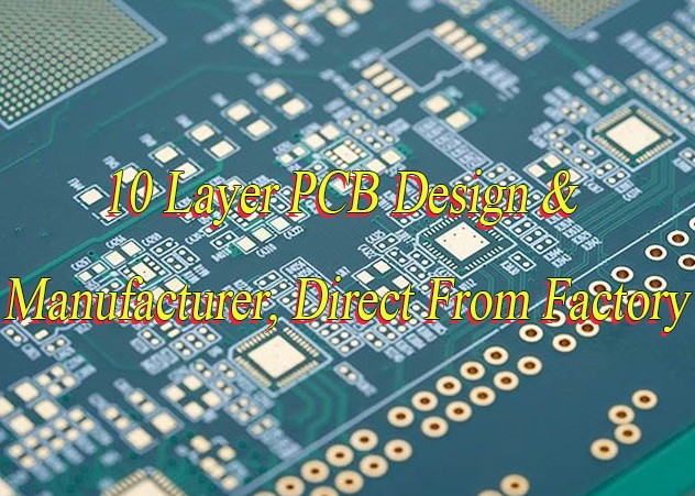
What is 10 layer PCB? Let’s discover its thickness, stackup, design spec and guide, production process, cost, difference between 8 layer PCB via this blog.
Are you troubled with these problems?
- Is controlling the alignment accuracy between layers in high-layer PCBs difficult, leading to unstable signal transmission?
- Are thermal management challenges in 10-layer boards affecting product performance and lifespan?
- Long lead times for small-batch, high-variety orders impacting project schedules?
As a 10 layer PCB manufacturer, EBest Circuit (Best Technology) can provide you service and solution:
- Innovative interlayer alignment technology ensuring zero signal loss in 10-layer board signal transmission;
- Intelligent thermal management solutions improving product heat dissipation efficiency by over 30%;
- A rapid-response production system enabling 7-day express delivery for small-batch orders.
Welcome to contact us if you have any inquiry for 10 layer PCB design and manufacturing: sales@bestpcbs.com.
What Is 10 Layer PCB?
A 10 layer PCB is a multilayer printed circuit board composed of ten layers of conductive copper foil and insulating material, stacked alternately. Its core advantage lies in achieving a more complex and high-density circuit layout within a limited space through this multilayer structure.
Compared to ordinary 2-layer or 4-layer boards, 10-layer PCBs offer superior performance in signal transmission speed, power distribution, and electromagnetic compatibility (EMC), effectively suppressing electromagnetic interference and improving system stability. They are commonly found in high-end communication equipment, servers, smartphones, and other applications with high performance and signal integrity requirements.
How Thick Is a 10 Layer PCB?
The thickness of a 10-layer PCB typically ranges from 0.8mm to 3.2mm, with 1.6mm being the most common standard thickness (accounting for approximately 60% of industry applications). Specific values are dynamically adjusted based on substrate type (e.g., FR-4, high-frequency materials), copper foil thickness (primarily 0.5oz for the inner layer and 1oz for the outer layer), and impedance control requirements. The tolerance range is generally ±10% of the nominal thickness. For example, the actual thickness of a 1.6mm board needs to be controlled between 1.44-1.76mm, while ultra-thin designs (0.8mm) are mostly used in mobile devices, and thicker boards (2.0mm and above) are suitable for high-power applications.
10 Layer PCB Stackup Example
| Layer Number | Layer Type | Description |
| 1 | Top Signal Layer | Low-speed signals, component placement |
| 2 | Ground Layer (GND) | Provides return path for top layer and layer 3 |
| 3 | High-Speed Signal Layer | Critical signals (e.g., clocks, differential pairs) |
| 4 | High-Speed Signal Layer | Orthogonal routing to layer 3 to reduce crosstalk |
| 5 | Power Layer (PWR) | Primary power distribution |
| 6 | Ground Layer (GND) | Forms tightly coupled power-ground plane with layer 5 |
| 7 | High-Speed Signal Layer | Same as layers 3 and 4, embedded between planes |
| 8 | High-Speed Signal Layer | Orthogonal routing to layer 7 |
| 9 | Ground Layer (GND) | Provides return path for layer 8 and bottom layer |
| 10 | Bottom Signal Layer | Low-speed signals, component placement |
Difference Between 8 Layer vs 10 Layer PCB
1. Layer Count and Structure
- 8 Layer PCB: 4 signal layers + 2 power/ground planes + 2 hybrid layers. Typical stackup alternates signal-power-ground-signal for balanced coupling.
- 10 Layer PCB: 6 signal layers + 3 power/ground planes + 1 shielding layer. Additional layers enable finer signal isolation and reference plane segmentation, e.g., high-speed layers embedded between planes.
2. Routing Capability and Density
- 8 Layer PCB: Medium complexity routing channels support BGA pitches ≥0.8mm, suitable for PCIe 3.0/4.0 interfaces.
- 10 Layer PCB: High-density routing supports BGA pitches ≤0.5mm, accommodating PCIe 5.0/6.0, DDR5, and other high-bandwidth interfaces with 20-30% more routing channels.
3. Signal Integrity (SI) and Electromagnetic Compatibility (EMC)
- 8 Layer PCB: Mid-frequency (≤5GHz) signals achieve low crosstalk via symmetric power-ground planes. EMI radiation meets standard limits.
- 10 Layer PCB: High-frequency (>10GHz) signals benefit from multi-layer reference planes, reducing crosstalk by 15-20dB and improving mixed-signal isolation. EMC immunity enhances.
4. Power Integrity (PI) and Thermal Management
- 8 Layer PCB: Dual power-ground planes support ≤10A current. Thermal management relies on inner copper foils, limiting temperature rise to ≤15°C.
- 10 Layer PCB: Triple-plane design reduces power impedance (≤1mΩ) and supports >15A current. Copper thickness accumulation improves thermal efficiency by 20%, reducing temperature rise to ≤10°C.
5. Cost and Manufacturing Lead Time
- 8 Layer PCB: Lower material costs by 20-30%, shorter lead time by 1-2 weeks, yield rate ≥95%. Ideal for mass production.
- 10 Layer PCB: Higher alignment complexity reduces yield to 90-93%, increases cost by 30-50%, and extends lead time by 2-3 weeks. Suitable for high-requirement projects.
6. Reliability and Mechanical Strength
- 8 Layer PCB: Sufficient durability for conventional industrial/consumer environments. Bending strength ≥200MPa.
- 10 Layer PCB: Enhanced reliability under vibration/thermal cycling. Bending strength ≥250MPa, ideal for automotive/aerospace applications.
7. Typical Application Scenarios
- 8 Layer PCB: Mid-to-high-end motherboards, network switches, automotive infotainment systems, industrial controls.
- 10 Layer PCB: High-performance servers, 5G base stations, medical imaging devices, high-speed test instruments.
8. Selection Recommendations
- 8 Layer PCB: Optimal for moderate complexity, cost-sensitive designs with signal speeds ≤5GHz.
- 10 Layer PCB: Preferred for dense high-speed links, fine-pitch BGAs, strict EMI/EMC requirements, or multi-power domains where performance outweighs cost.
10 Layer PCB Design Technical Requirements
| Parameters | Typical Value/Range |
| Standard Thickness | 1.6mm (±10%) |
| High-Frequency Material Thickness | 0.8-2.4mm |
| Substrate Type | FR-4 / Rogers RO4350B Hybrid |
| Inner Layer Min Trace Width/Spacing | 4/4mil (0.1mm) |
| Outer Layer Recommended Trace Width/Spacing | 5/5mil |
| Copper Thickness Configuration | Inner: 1oz (35μm) / Outer: 1.5oz (50μm) / Power: 2oz (70μm) |
| 50Ω Microstrip (Outer Layer) | Trace Width: 8mil (Dielectric: 5mil) |
| 50Ω Stripline(Inner Layer) | Trace Width: 5mil (Dielectric: 4mil) |
| Impedance Tolerance | ±10% |
| Mechanical Drill Limit | 0.2mm |
| Laser Drill Limit | 0.1mm |
| Via Aspect Ratio | ≤8:1 (0.2mm hole at 1.6mm thickness) |
| Preferred Routing Layers | Layer 3 / Layer 8 (Signal Layers) |
| Symmetrical Stackup | Top-Gnd-Sig-Pwr-Gnd-Sig-Gnd-Pwr-Sig-Bottom |
| Surface Finish | ENIG / Immersion Gold (0.05-0.1μm) |
| Solder Mask Bridge Min Width | 3mil |
10 Layer PCB Design Guideline
Below is a detailed guide for 10 layer PCB design:
1. Layer Stackup Planning
- Standard Configuration: Recommend “Signal-GND-Power-Signal-Signal-Power-GND-Signal-GND-Signal” structure (Top to Bottom) to ensure symmetry and minimize warpage. Prioritize power and ground layers in the middle to form shielding cavities and suppress EMI.
- Layer Thickness Allocation: Core signal layers require 50±5Ω impedance control. Power/ground layers thickness ≥0.2mm to reduce plane impedance. Use low-loss FR4 (Df≤0.008) or high-speed materials (e.g., Panasonic Megtron 6).
- Reference Planes: High-speed signal layers must neighbor complete reference planes (ground or power). Differential pairs maintain ≥20mil spacing and avoid crossing split planes.
2. Power Integrity (PI) Design
- Power Plane Partitioning: Segment independent power domains (digital/analog/RF) per functional modules. Use stitching capacitors (100nF+10μF combo) across splits with ≤10mm spacing.
- Decoupling Capacitor Placement: Position high-frequency decoupling caps (0.1μF ceramic) within 5mm of IC power pins. Bulk capacitors (100μF) placed at board edges form low-frequency energy storage networks.
- Plane Resonance Suppression: Grid-pattern power planes or embedded capacitor materials avoid >200MHz plane resonance. Validate critical planes via 3D simulation (e.g., Ansys SIwave).
3. Signal Integrity (SI) Optimization
- Impedance Control: Single-ended signals at 50Ω, differential at 100Ω±10%. Calculate trace width/spacing via Polar SI9000. High-speed signals (e.g., DDR5, PCIe 4.0) require continuous impedance without discontinuities.
- Crosstalk Mitigation: Maintain ≥3W spacing (W = trace width). Sensitive signals (e.g., clocks) use shielded differential pairs or guard traces. Length matching error ≤5mil.
4. Electromagnetic Compatibility(EMC) Design
- Shielding & Grounding: RF modules use metal shields with ≥20 pads/cm² grounding density. Chassis ground connects to PCB ground via conductive adhesive/spring contacts (contact resistance <10mΩ).
- Filtering: Add common-mode chokes (100μH) and X/Y capacitors (0.1μF) at input power ports to suppress conducted noise. High-speed interfaces (e.g., USB3.0) include common-mode filters.
- Grounding Strategy: Mixed grounding (digital/analog grounds connected at a single point near noise sources). Board edges feature 20mil-wide ground rings for low-impedance return paths.
5. Thermal Management & Reliability
- Heat Dissipation: High-power devices (e.g., FPGA) use ≥2oz copper under pads with thermal via arrays (12mil diameter, 20mil pitch). Thermally sensitive components stay clear of heat sources.
- Thermal Stress Relief: BGA devices adopt checkerboard routing to avoid CTE mismatch. Board edges include stress-relief slots to prevent solder cracking.
- Pad Design: QFN/BGA pads use non-solder mask defined (NSMD) with pads 10-15% smaller than package size. Through-hole pads add thermal relief to minimize solder voids.
6. Design for Manufacturing (DFM) & Testability (DFT)
- DFM Rules: Minimum trace/space ≥4mil (100μm), via size ≥8mil/16mil (pad/hole). Blind/buried vias evaluate cost; prefer HDI (e.g., 2+8+2 structure).
- DFT Design: Critical signals include test points (≥1mm diameter, ≥200mil spacing). Board edges reserve JTAG ports compatible with ATE equipment.
- File Specifications: Gerber outputs include stackup tables, impedance reports, and drill files. Provide 3D STEP models for mechanical assembly validation.
7. High-Speed Digital Design
- Differential Pair Routing: Equal length (error ≤5mil), GND guard traces, spacing ≥3× differential gap. Avoid split planes; prioritize inner layers.
- Clock Distribution: Clock sources near loads with star topology. Clock lines use GND shielding; length matching error ≤1mm (corresponds to 100ps timing error).
- Simulation Validation: Use HyperLynx/ADS for signal integrity analysis, focusing on eye diagram margin (≥50% UI) and S-parameter resonance.
8. Power Management Circuitry
- DC/DC Layout: Switching regulators place input capacitors near modules to minimize loop area. Power inductors prohibit routing underneath to avoid EMI.
- LDO Design: LDO outputs pair low-ESR tantalum (10μF) and ceramic (100nF) capacitors to suppress oscillation.
- Power Monitoring: Critical rails include voltage monitor points for debugging. Reserve test points (TP) for production testing.
9. Analog & RF Design
- Low-Noise Design: Sensitive analog circuits (e.g., ADC drivers) use dedicated ground planes to avoid digital noise coupling. Use temp-stable resistors (±1%) and precision capacitors (C0G).
- RF Routing: 50Ω microstrip lines control thickness (H=dielectric height) with ≤5% impedance error. RF modules use metal shielding with dense ground pads.
- Antenna Isolation: RF antenna areas stay clear of digital signals with GND shielding. Antenna feeds include π-matching networks for impedance tuning.
10. Documentation & Collaboration
- Design Documentation: Include complete BOM (part number, package, supplier), stackup tables, impedance calculations, and simulation summaries.
- Version Control: Use Git/SVN for design file version tracking to ensure traceability.
- Cross-Team Collaboration: Regular sync with hardware/structural/test engineers to align design with system requirements.
10 Layer PCB Fabrication Process
1. Design Data Verification and Process Planning
- Design Specification Check: Verify line width, spacing, and interlayer alignment accuracy against IPC-6012 standards. Validate minimum line width/spacing ≥75μm, interlayer/layer spacing tolerance ≤±20μm, and layer alignment error ≤50μm using AOI systems for automatic Gerber-to-actual deviation analysis.
- Material Selection Confirmation: Determine core material models (e.g., FR4-Tg170/RO4350B), prepreg types (1080/2116/7628), and copper foil thickness (1/2OZ/3OZ) based on application requirements (high-frequency/high-speed/high-power/heat-resistant). Validate thermal expansion coefficient matching.
- Process Flow Planning: Develop a 28-step detailed process route map highlighting critical control points (e.g., lamination temperature profiles, plating current densities) and special process requirements (blind/buried via fabrication, back-drilling depth control).
- Impedance Calculation Verification: Utilize Polar SI9000 tools to calculate stackup impedance values (single-ended 50Ω/differential 100Ω). Optimize stackup structure considering dielectric thickness tolerance (±5%) and dielectric constant (εr=4.2±0.3) to ensure TDR measurement deviation ≤±10%.
2. Inner Layer Image Transfer
- Substrate Preparation: Process double-sided copper-clad laminates through mechanical brushing (brush pressure 1.5kg/cm²) and chemical cleaning (acid wash → water rinse → microetching). Achieve surface roughness Ra≤0.5μm and copper surface cleanliness per IPC-TM-650 standards.
- Dry Film Lamination: Apply photoresist dry film (15-25μm thickness) in a Class 1000 cleanroom using roller lamination at 2-4kg/cm² pressure, 35-45℃ temperature, ensuring no bubbles or wrinkles.
- Exposure Imaging: Employ LDI laser direct imaging (355nm wavelength) with 70-90mJ/cm² exposure energy and ±10μm alignment accuracy for residue-free pattern transfer.
- Developing Process: Use sodium carbonate solution (1.0±0.1% concentration) at 30±2℃ for 45-60 seconds. Ensure line width deviation ≤±5% and no residual film defects post-development.
- Acid Etching: Utilize cupric chloride etchant (180g/L CuCl₂, 2.5N HCl) at 45±2℃ with 1.8-2.2m/min conveyor speed. Achieve etching factor ≥2.0 and undercut ≤10%.
- Strip Process: Remove cured dry film using sodium hydroxide solution (3-5% concentration) at 50±3℃ for 1-2 minutes, ensuring no residual film affecting subsequent processes.
3. Inner Layer Automated Optical Inspection
- Defect Detection: Utilize 20-megapixel CCD cameras for automatic detection of opens (≥50μm), shorts (≥30μm), and notches (depth ≥1/4 line width) with ±2μm accuracy.
- Data Comparison: Perform pixel-level comparison between inspection images and original Gerber data, generating defect maps with coordinate annotations. Support CAD data import and automated repair recommendations.
- Defect Marking: Mark non-conforming points using UV laser marking (2W power, 20kHz frequency) with 0.5×0.5mm dimensions for manual re-inspection or automated repair equipment targeting.
4. Lamination Molding
- Stackup Structure: Assemble “copper foil-prepreg-inner core-prepreg-copper foil” sequence with 0.1mm PET release film between layers to prevent adhesion. Maintain stack thickness tolerance ±3%.
- Pre-lamination Alignment: Secure interlayer alignment using rivet positioning (±0.03mm accuracy) or hot-melt adhesive curing (180℃/3 seconds). Ensure interlayer alignment error ≤50μm.
- Hot Pressing: Implement segmented heating (120℃/30min→150℃/60min→180℃/90min) and progressive pressure application (50-100kg/cm²) in vacuum press. Achieve full prepreg curing with glass transition temperature Tg≥150℃.
- Cooling Pressure Maintenance: Control cooling rate 1-2℃/min while maintaining pressure until temperature drops below 40℃ to prevent thermal stress-induced warpage (warpage ≤0.75%).
5. Mechanical Drilling
- Drilling Parameter Setting: Optimize spindle speed (8000-30000rpm) and feed rate (0.5-3.0m/min) based on hole diameter (0.2-6.0mm), board thickness (0.8-6.0mm), and material properties. Implement segmented drilling to reduce tool wear.
- Cover/Backing Plate Utilization: Combine aluminum cover plates (1.5mm thickness) with composite backing plates (phenolic resin + fiberglass) to ensure burr-free hole entries and smooth chip removal. Achieve hole wall roughness Ra≤3.2μm.
- Hole Position Accuracy Control: Employ high-precision CNC drilling machines (±0.05mm positional accuracy) with laser alignment systems (±10μm accuracy) for precise hole positioning. Maintain hole position deviation ≤50μm.
- Hole Wall Quality Inspection: Validate hole wall integrity through metallographic cross-section analysis—no delamination, no smear. Ensure hole copper uniformity ≥85% and metallization thickness ≥20μm.
6. Hole Metallization
- Electroless Copper Plating: Perform desmearing (potassium permanganate), palladium activation (50ppm Pd²⁺), and electroless copper deposition (0.8g/L Cu²⁺) to form 0.3-0.5μm copper layers at 0.2μm/min deposition rate. Achieve ≥5B adhesion strength.
- Full Board Plating: Use acidic sulfate copper electrolyte (60g/L CuSO₄, 180g/L H₂SO₄) at 2.0A/dm² current density for 45 minutes to thicken hole copper to 20-25μm. Maintain plating uniformity ±10%.
- Hole Wall Quality Testing: Evaluate hole copper coverage (≥90%) via backlight testing (grades 1-10) and verify uniformity/pinhole-free integrity through cross-section analysis. Ensure electrical connection reliability.
7. Outer Layer Image Transfer
- Secondary Dry Film: Apply photoresist film (20-30μm thickness) to electroplated copper surfaces using vacuum laminators for bubble-free adhesion. Maintain 3-5kg/cm² pressure at 40±2℃.
- Outer Layer Exposure: Implement high-precision alignment systems (±5μm accuracy) for outer layer pattern transfer using 80-100mJ/cm² exposure energy. Ensure sharp edges without residual images.
- Pattern Plating: Sequentially plate copper layers (25-30μm thickness at 3.0A/dm²) and tin protective layers (5-8μm thickness). Tin serves as etch resist for subsequent processes.
- Strip and Etch: Remove resist using sodium hydroxide solution followed by alkaline etching (150g/L CuCl₂, 200g/L NH₄Cl) to remove non-circuit copper. Achieve etching factor ≥2.5 and line width deviation ≤±5%.
8. Solder Mask and Surface Finish
- Solder Mask Application: Apply liquid photoimageable solder mask (20-30μm thickness) via screen printing (120 mesh) or coating processes. Ensure mask extends 0.1mm beyond pad areas without bubbles/pinholes.
- Solder Mask Exposure: Use UV exposure (300-500mJ/cm² energy) to define pad openings. Cured mask must withstand 24h solvent resistance and thermal shock (288℃/10s) without cracking.
- Legend Printing: Print component identifiers, board numbers, and version info using epoxy ink (15-20μm thickness) with ±0.1mm accuracy and clear, smear-free lettering.
- Surface Finish Selection: Choose ENIG (3-5μm Au/5-7μm Ni), HASL (5-8μm SnPb), immersion silver (2-4μm Ag), or OSP (0.3-0.5μm organic solderability preservative) per requirements. Ensure solderability meets IPC-J-STD-001 standards.
9. Electrical Testing and Final Inspection
- Continuity Testing: Verify circuit continuity (≤1Ω resistance) and insulation (≥100MΩ resistance) using flying probe (50μm probe pitch) or bed-of-nails testers. Achieve 100% test coverage.
- Impedance Testing: Sample-test characteristic impedance values (single-ended 50±5Ω/differential 100±10Ω) at 1GHz frequency using TDR equipment. Ensure signal integrity compliance.
- Dimensional Inspection: Validate form dimensions (±0.1mm), hole position accuracy (±0.05mm), and thickness uniformity (±3%) using coordinate measuring machines per IPC-A-600 standards.
- Visual Inspection: Conduct visual and microscopic examinations per IPC-A-600 standards to verify absence of scratches, dents, foreign materials, oxidized pads, and legible markings. Target final yield ≥99.5%.
Why Choose EBest Circuit (Best Technology) as 10 Layer PCB Manufacturer?
Below are reasons why choose us as 10 layer PCB manufacturer:
- 19 Years of Expertise: Decades of high-layer PCB manufacturing experience with a proprietary production error database, enabling proactive risk mitigation and cost reduction for clients.
- Global Certification Compliance: Certifications including ISO 9001, IATF 16949 automotive standards, medical-grade compliance, and RoHS ensure adherence to international market requirements.
- Cost-Sensitive Solutions: Competitive pricing with tailored cost optimization strategies for client designs, directly reducing project expenses and enhancing market competitiveness.
- 24 Hour Rapid Prototyping: Urgent orders supported by accelerated prototyping services, ensuring market-first opportunities and shortened time-to-market cycles.
- Free DFM Analysis: Complimentary Design for Manufacturability reviews to identify and resolve manufacturability issues early, reducing redesign costs and improving production efficiency.
- 99.2% On-Time Delivery: High-precision delivery management with 99.2% order fulfillment rate, safeguarding production schedules and minimizing delay-related costs.
- 100% Batch Inspection: Stringent quality control with full-batch inspection for mass production, backed by ISO 9001, IATF 16949, medical-grade, and RoHS certifications to ensure defect-free delivery.
- Data-Driven Process Optimization: Leveraging a 19-year production error database for predictive process adjustments, delivering stable and cost-effective manufacturing solutions.
- Scalable Production Capacity: Flexible capacity management from prototyping to volume production, ensuring seamless transitions and avoiding capacity-related delays.
- End-to-End Service Support: Full lifecycle support from design consultation and prototyping to mass production and post-sales tracking, maximizing client ROI and project value.
How Much Does A 10-Layer PCB Cost?
The price of a 10-layer PCB varies significantly depending on the material specifications, manufacturing complexity, and order quantity. For example, using standard FR-4 material, 1 oz copper thickness, and ENIG surface treatment, a small batch (e.g., 10 boards) of 10-layer boards would cost approximately $220 per square meter. In mass production (e.g., over a thousand boards), the price can drop to $15–$25 per board due to economies of scale (assuming a board area of approximately 0.1 square meters). Actual pricing will depend on specific design requirements such as trace width/spacing, via diameter, blind/buried vias, and impedance control. You can directly provide drawings to a professional PCB manufacturer like EBest Circuit (Best Technology) to get an accurate quote. Contact us now: sales@bestpcbs.com.