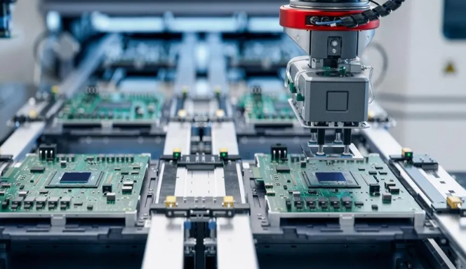
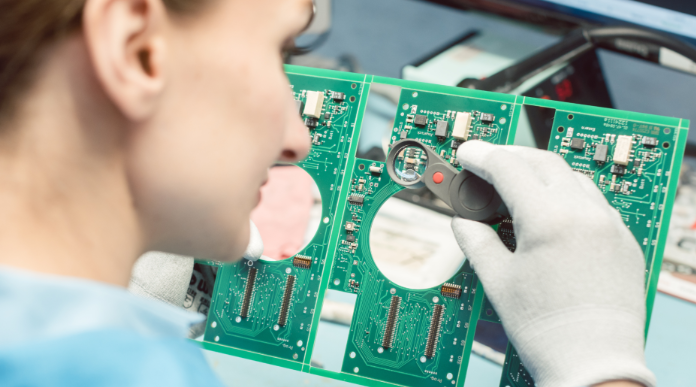
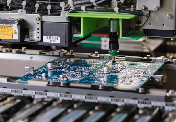
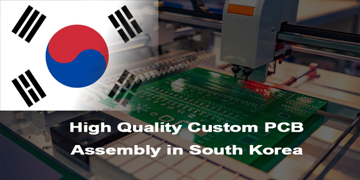
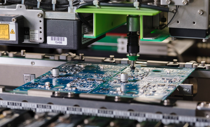
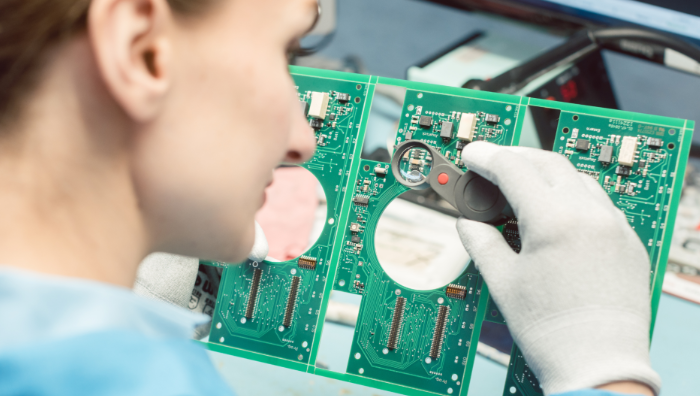
High-quality PCB assembly in South Korea integrates advanced manufacturing technologies including those for BT packaging substrates and AiP substrates with rigorous quality control to meet diverse industry demands. Supported by mature industrial clusters and global supply chain integration, PCB assembly in South Korea caters to key sectors like electronics, automotive, and medical, delivering reliable products that balance performance, efficiency, and industry-specific standards.
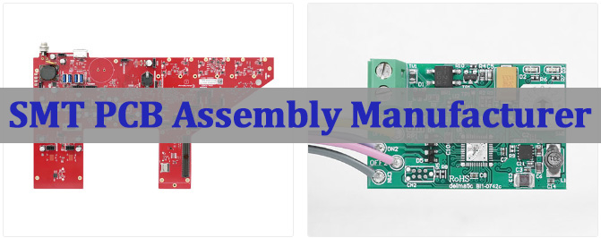
Top 10 PCB Assembly Manufacturer in South Korea
| Company Name | Advantage | Assembly Capability | Delivery Lead Time |
| EBest Circuit Co., Limited | 19-year experience, ISO9001/AS9100D/IATF16949 certified, MES system, one-stop service | 2-30 layers, HDI, rigid-flex, SMT, BGA mounting, 0402 components, AOI/X-Ray inspection | 24hrs (urgent), 3-5 days (standard), 25 days (mass production) |
| BHflex | Rigid-flex PCB specialist, IVH/HDI tech, global branches, automotive/medical focus | 2-24 layers, flexible/rigid-flex PCBA, fine-pattern FPCB, SMT assembly, functional testing | 72hrs (urgent), 4-7 days (standard), 28 days (mass production) |
| Daeduck Electronics | 50+ years experience, ultra-thin PCBA expert, semiconductor packaging, ISO9001/IATF16949 | 2-28 layers, ultra-thin PCBA, CSP/FCCSP packaging, SMT, X-Ray inspection | 48hrs (urgent, simple layers), 5-8 days (standard), 30 days (mass production) |
| ISU Petasys | Listed company, ultra-multilayer PCBA, global factories, 900+ employees, network focus | 2-40 layers, ultra-high integration PCBA, SMT/BGA, network equipment assembly | 72hrs (urgent), 6-10 days (standard), 35 days (mass production) |
| KMTS (Kwang Myung Tech Solution) | Seoul-based, one-stop service, ISO9001/ISO14001, OEM/ODM support, cost-effective | 2-16 layers, rigid PCBA, SMT assembly, AOI/X-Ray testing, component sourcing | 48hrs (urgent), 3-6 days (standard), 22 days (mass production) |
| Ace Tech Circuit (ATC) | Gyeonggi-based, AS9100/ISO14001, burn-in PCBA, high-temperature material expertise | 2-100 layers, rigid PCBA, FR-4/polyimide/PTFE, SMT, burn-in testing | 72hrs (urgent, ≤10 layers), 5-9 days (standard), 32 days (mass production) |
| Bluetop | Gyeonggi-do based, HDI PCBA specialist, medical/telecom focus, ceramic materials | 2-42 layers, HDI/rigid PCBA, medical device assembly, SMT, sterility testing | 5 days (urgent), 4-8 days (standard), 26 days (mass production) |
| EOS Corporation | Aerospace/automotive focus, ISO9001/AS9100D, flexible/HDI PCBA expertise | 2-42 layers, flexible/hybrid PCBA, automotive electronic assembly, vibration testing | 72hrs (urgent, automotive), 6-10 days (standard), 30 days (mass production) |
| Flexon | Gyeonggi-based, rigid-flex/flexible PCBA, polyimide materials, small-batch focus | 2-12 layers, flexible/rigid-flex PCBA, SMT, small-batch assembly, functional testing | 4 days (urgent), 3-7 days (standard), 20 days (mass production) |
| Interflex Co., Limited | Automotive/medical focus, rigid-flex PCBA, one-stop assembly, industry compliance | 2-20 layers, rigid/rigid-flex PCBA, automotive/medical assembly, SMT, AOI testing | 5 days (urgent), 5-8 days (standard), 27 days (mass production) |
Pain Points of PCB Assembly in South Korea
- Is it difficult to get urgent PCB prototyping with a lead time shorter than 3 days in South Korea?
- Is it challenging to find manufacturers that offer both high-precision HDI PCB assembly and reliable prototyping?
- Do many manufacturers lack transparent production tracking for PCB assembly orders in South Korea?
- Is it hard to ensure consistent quality across small-batch and large-scale PCB assembly in South Korea?
- Do supply chain delays often affect the delivery of PCB assembly prototypes in South Korea?
- Is it expensive to get PCB assembly prototypes that meet medical or aerospace industry standards?
- Do many manufacturers fail to provide timely technical support for custom PCB assembly requests?
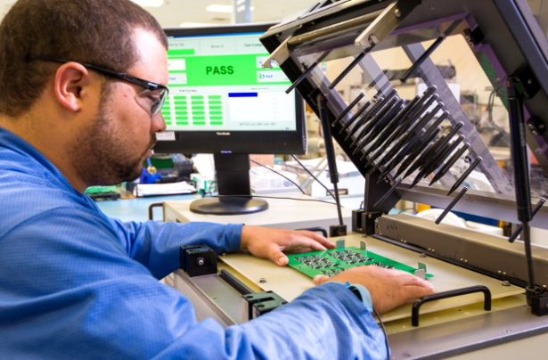
Why Choose EBest(Best Technology) for PCB Assembly in South Korea?
Reasons why choose EBest( Best Technology) for PCB assembly in South Korea partner:
- Urgent Prototyping Solution: Our 24-hour fast prototyping and delivery is 30% faster than the industry average, getting your prototypes in record time without delays.
- 19 Years of Proven PCB Expertise: With 19 years of experience in PCB production and over 5,000 global clients across electronics, medical and automotive sectors, we master tailored solutions for sector-specific pain points.
- Strict Quality Control You Can Trust: Certified with ISO9001, AS9100D and IATF 16949, we maintain a 99.8% product qualification rate to ensure consistent quality for both small-batch trials and large-scale production while meeting global industry standards.
- One-Stop PCB Assembly in South Korea (Turnkey Service): We cover every step from design review and component sourcing to assembly and testing, eliminating the hassle of coordinating with multiple suppliers. This cuts coordination time by 40%, letting you focus on your core projects.
- Transparent Production Tracking: Our MES system provides real-time production data tracking, allowing you to monitor your order’s progress anytime, anywhere. Enjoy full visibility and peace of mind throughout the process with no guesswork or hidden delays.
- Cost-Effective Solutions for Rising Costs: Our bulk component sourcing channels slash material costs by 15% without sacrificing quality. This effectively mitigates the pressure of rising gold, copper and component prices, helping you stay within budget while maintaining product excellence.
- High-Precision Assembly Capabilities: We support 2-30 layers, HDI, BGA and 0402 component assembly, ideal for high-end, precision-driven projects. Our advanced processes ensure stable signal transmission and long-term product reliability to meet even the strictest high-precision demands.
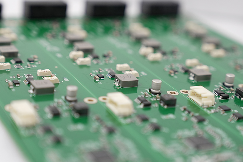
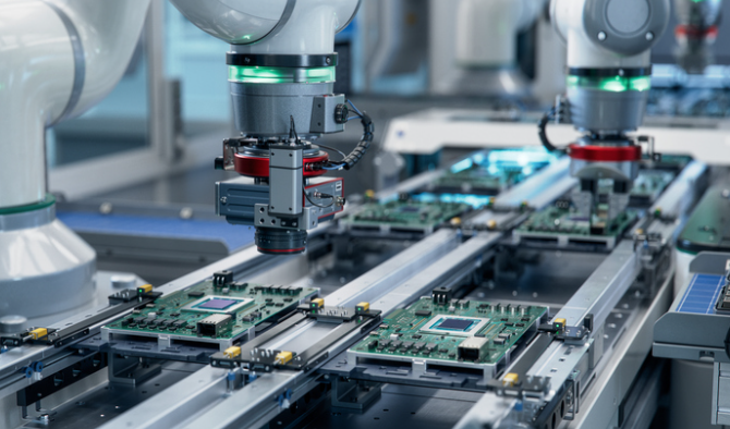
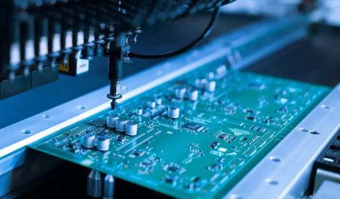
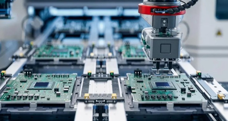
Types of Custom South Korea PCB Assembly Service We Offered
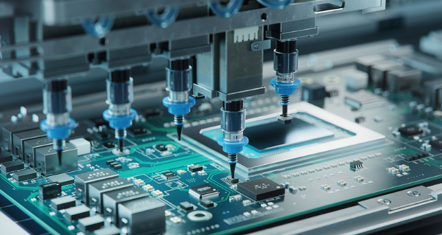
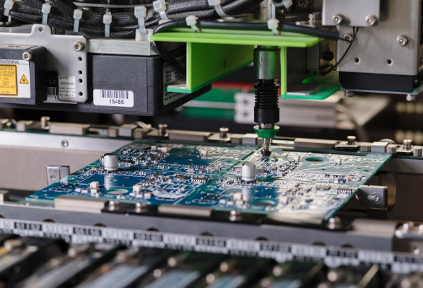
- Surface Mount Technology (SMT) Assembly: High-precision placement of components on PCB surfaces, supporting single/double-sided SMT.
- Through-Hole Technology (THT) Assembly: Manual or automated insertion of components with leads through PCB holes.
- Mixed SMT/THT Assembly: Combination of SMT and THT processes for hybrid circuit designs.
- BGA/QFN Assembly: Precision placement of Ball Grid Array (BGA) and Quad Flat No-Lead (QFN) packages with X-ray inspection.
- Quick-Turn Prototyping: Rapid prototype assembly (3–5 days) for fast design validation.
- Mass Production Assembly: Scalable high-volume production with 7–10-day lead times.
- Testing Services: AOI (Automated Optical Inspection), X-ray, ICT (In-Circuit Test), and FCT (Functional Circuit Test).
- Eco-Friendly Processes: Lead-free soldering, RoHS compliance, and low-energy manufacturing.
- Custom Design Support: DFM (Design for Manufacturability) analysis, impedance control, and thermal/EMC optimization.
- Supply Chain Management: End-to-end component sourcing, logistics, and one-stop PCBA (PCB Assembly) services.
- Specialty Material Handling: Support for Rogers/Taconic substrates, metal-core PCBs, and high-temperature materials.
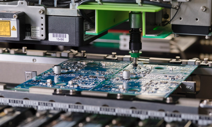
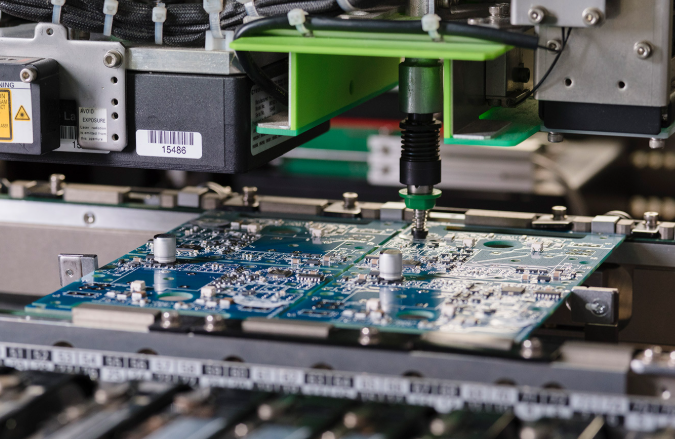
Our Quality Control Process for South Korea PCBA Orders
Below are our quality control process for South Korea PCB Assembly orders:
- Incoming Material Inspection: 100% inspect PCB substrates, electronic components and solder paste, verifying key parameters such as substrate thickness, component batch consistency and solder paste viscosity to ensure full compliance with customer specifications and RoHS standards, which eliminates quality risks from the source.
- Design Review: Conduct detailed DFM (Design for Manufacturability) analysis before production, focusing on pad size rationality, component spacing and via layout, and optimize designs for easier assembly and testing to avoid manufacturability issues and reduce rework time.
- In-Process Inspection: Conduct multi-stage testing after SMT and reflow soldering. AOI detects common surface defects like component misalignment, missing parts and cold joints, while X-Ray targets hidden defects in fine-pitch components such as BGA to prevent quality hazards.
- Electrical Testing: 100% ICT and FCT testing is performed on all finished PCBA. ICT verifies circuit continuity, detects open circuits, short circuits and incorrect component installation, while FCT simulates real working conditions to ensure functional performance meets operational requirements.
- Environmental Testing: Conduct strict environmental tests for high-reliability orders such as medical and aerospace PCBA, including temperature and humidity cycling, vibration and aging tests, to ensure long-term stability when products operate in harsh environments.
- Final Inspection: Perform comprehensive visual, packaging and documentation reviews on finished products. Visual inspection checks for surface scratches and poor soldering; packaging review ensures anti-static and moisture-proof protection; documentation review confirms all compliance reports are complete.
- Traceability Management: Our MES system records real-time production and inspection data, including raw material batch numbers, production parameters and test results. Each PCBA is assigned a unique traceability code to enable full-lifecycle tracking, which facilitates quick problem location and analysis if issues arise.
Our South Korea PCB Assembly Capabilities
| Item | Capabilities |
| Placer Speed | 13,200,000 chips/day |
| Bare Board Size | 0.2 x 0.2 inches – 20 x 20 inches/ 22*47.5 inches |
| Minimum SMD Component | 01005 |
| Minimum BGA Pitch | 0.25mm |
| Maximum Components | 50*150mm |
| Assembly Type | SMT, THT, Mixed assembly |
| Component Package | Reels, Cut Tape, Tube, Tray, Loose Parts |
| Lead Time | 1 – 5 days |
Case Studies of Our South Korea Medical PCB Assembly
We partnered with Seoul Medical Devices Co., Ltd., a local South Korean medical equipment maker, to provide custom PCB assembly in South Korea for their new portable blood glucose monitor. The client specializes in high-precision clinical diagnostic devices and aims to enter the Southeast Asian market, where Singaporean buyers value proven case references and strict quality compliance.
Project Background: The client specializes in portable clinical diagnostic equipment, and its new portable blood glucose monitor is for hospital outpatient and home care use. It requires stable PCB performance to ensure accurate blood glucose readings (error margin ≤ ±5%). The client chose our PCB assembly in South Korea service for our ISO13485 certification, Class 10000 cleanroom production, and local supply chain advantages, which meet its strict medical compliance and tight delivery needs.
Project Requirements: The project had strict requirements: ISO13485-aligned production for full traceability and contamination control, 10-layer rigid-flex PCBA assembly with 0402 small-pitch components, a minimum 99.9% yield rate, 8-day prototyping for design verification, and 22-day mass production delivery to support its Southeast Asian launch.
Project Challenges: The project had three key challenges: an 8-day prototyping timeline (including design review, medical component sourcing, assembly and testing) that is 30% faster than the industry average, strict compliance with KFDA, ISO13485 and RoHS standards requiring certified components and contamination-free assembly, and high precision for 0402 components (±0.03mm placement accuracy) to ensure stable signal transmission.
Our Solutions: We implemented targeted solutions to address these challenges: a dedicated medical PCB assembly team with over 5 years of experience in KFDA and ISO13485 compliance, a local medical component supply chain to cut sourcing time by 2 days, an expedited production line and Class 10000 cleanroom for medical production, MES system for full production traceability, and detailed DFM analysis to ensure 0402 component placement precision.
Results: Our solutions delivered exceptional results that exceeded the client’s expectations and fully met the standards valued by Singaporean buyers. The prototype was delivered in 6 days, 2 days ahead of the 8-day requirement, allowing the client ample time to complete design verification. The mass production yield rate reached 99.96%, surpassing the 99.9% minimum requirement, with only 23 minor appearance defects out of 5000 units all of which were reworked to meet medical standards. Mass production was delivered in 20 days, 2 days ahead of the 22-day schedule, supporting the client’s timely launch in Southeast Asia. The client successfully passed KFDA, CE MDR and FDA 510(k) certifications.
FAQs of PCB Assembly in South Korea
Q1: Is it possible to get urgent PCB prototyping in South Korea with a 24-hour lead time, especially for multi-layer boards?
A1: Yes, we offer 24-hour urgent PCB prototyping for simple 2-layer boards, which fully meets the urgent project needs. For 4-8 layer boards, we can complete prototyping within 48-72 hours, and for 10+ layer high-precision boards, the urgent lead time is 5 days. Our expedited production line and local component supply chain ensure fast delivery without compromising quality.
Q2: With the continuous rise of raw material prices such as gold and copper, how can we reduce the cost of PCB prototyping in South Korea?
A2: We help clients control prototyping costs through two core ways. First, our bulk component sourcing channels can reduce raw material costs by 15% without sacrificing quality. Second, we provide cost-saving material options for non-critical prototypes, while offering free DFM analysis to avoid rework costs caused by design problems.
Q3: What should I do if there are design defects in the PCB prototype after delivery, which affects the follow-up test progress?
A3: We take proactive and efficient measures to solve this problem. Before prototyping production, we provide free DFM (Design for Manufacturability) analysis to identify and optimize potential design defects in advance. If minor design issues still occur after delivery, we offer free rework within 24 hours and assign professional engineers to provide technical support for design optimization.
Q4: Can I track the production progress of my PCB prototyping order in real time to avoid uncertainty about the delivery time?
A4: Yes, you can track the progress in real time. Our MES production management system records every link of prototyping, including material incoming, SMT assembly, testing and packaging. You can check the detailed progress, inspection results and estimated delivery time at any time through our client portal, without the need for repeated consultation.
Q5: If I need PCB prototyping that meets medical industry standards, can manufacturers in South Korea quickly meet the relevant compliance requirements?
A5: Yes, we can fully meet your needs. Our medical PCB prototyping is fully aligned with ISO13485 standards, with Class 10000 cleanroom production, strict contamination control and reliability testing. We have rich experience in medical prototyping and can complete the production and compliance testing of medical-grade prototypes within the standard lead time, supporting your product certification progress.