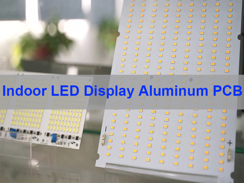
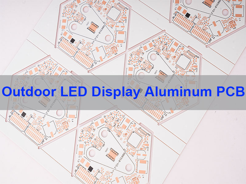
Why Choose EBest for Your LED Strip Light Aluminum PCB Needs?
EBest is your trusted partner for high-quality LED Strip Light Aluminum PCB, with 19+ years of industry experience and proven expertise in delivering reliable, high-performance solutions. Our LED Strip Light Aluminum PCB products meet strict industry standards, ensuring optimal performance for all your lighting projects.
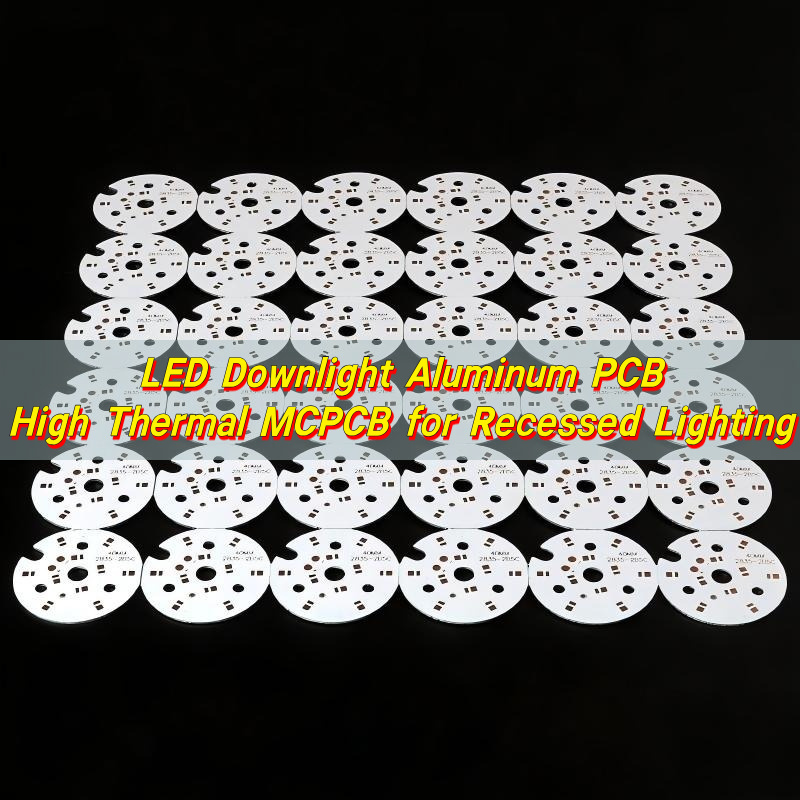
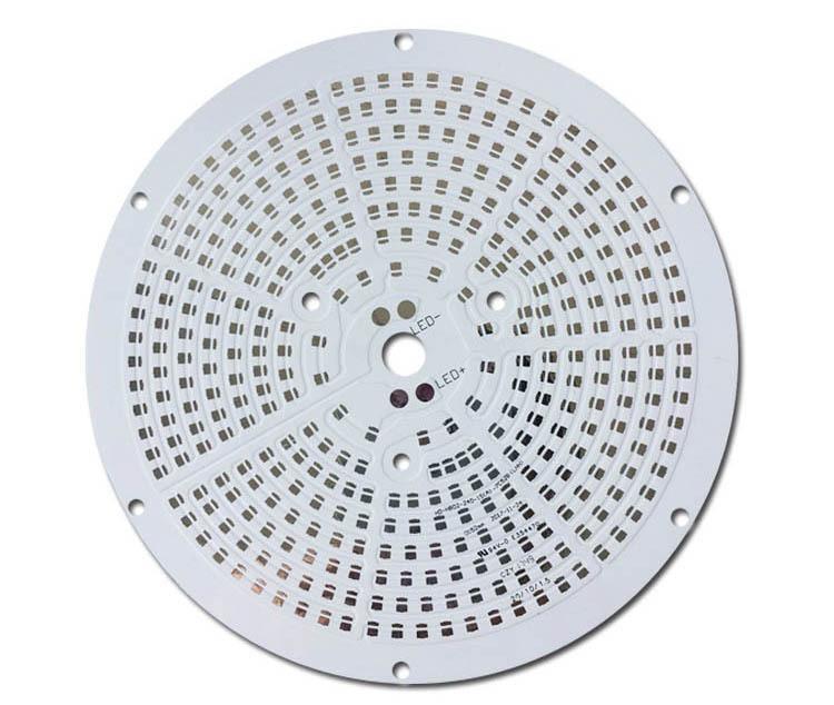
Core parameters of our LED Strip Light Aluminum PCB: Thermal conductivity up to 2.0-3.0 W/(m·K), copper foil thickness 1oz-10oz, aluminum base material (6061/5052/1060), insulation layer thickness 50-150μm, operating temperature range -40℃ to 85℃, and compliance with RoHS/UL standards. Order from EBest today for stable supply, fast delivery, and professional support.
Why Choose EBest for LED Strip Light Aluminum PCB?
- Quality: Our LED Strip Light Aluminum PCB undergoes 100% full inspection before delivery, with strict quality control processes and certifications to ensure consistency and reliability. We use A+ grade materials and advanced manufacturing techniques to avoid common issues like poor heat dissipation and circuit failure.
- Delivery: With a monthly production capacity of 260,000 square feet (28,900 square meters), we guarantee fast turnaround times. Urgent orders for LED Strip Light Aluminum PCB can be shipped within 24 hours, meeting your tight project deadlines.
- Service: We offer one-stop solutions for LED Strip Light Aluminum PCB, including custom design, prototype production, mass manufacturing, and after-sales support. Our team provides personalized guidance to solve your specific project challenges.
- Supply Chain: We have a stable and perfect supply chain for all components related to LED Strip Light Aluminum PCB, ensuring consistent material quality and on-time delivery without supply risks.
What Are the Key Pain Points of LED Strip Light Aluminum PCB, and How Does EBest Solve Them?
Many users face common challenges with LED Strip Light Aluminum PCB, including poor heat dissipation, unstable performance, inconsistent quality, and delayed delivery. EBest addresses each pain point with targeted solutions to ensure your projects run smoothly.
- Pain Point 1: Poor heat dissipation leading to LED light decay and short lifespan.
Solution: Our LED Strip Light Aluminum PCB uses high-thermal-conductivity aluminum bases and optimized copper foil design, including extended heat pads and full散热过孔, to reduce thermal resistance and keep LED junction temperatures below 70℃.
- Pain Point 2: Inconsistent circuit performance and color deviation.
Solution: We use precision etching processes (error ±5μm) and independent current-limiting designs for each LED, ensuring uniform current distribution and consistent light output across the entire strip.
- Pain Point 3: Quality inconsistencies and high failure rates.
Solution: Every batch of our LED Strip Light Aluminum PCB undergoes strict testing, including thermal resistance, voltage resistance, and circuit continuity checks, with a failure rate below 0.1%.
- Pain Point 4: Delayed delivery and supply chain disruptions.
Solution: Our stable supply chain and large production capacity ensure on-time delivery, even for large orders. We also offer expedited service for urgent LED Strip Light Aluminum PCB needs.
Choose EBest for your LED Strip Light Aluminum PCB projects, and let us solve your pain points with our professional solutions and reliable service.
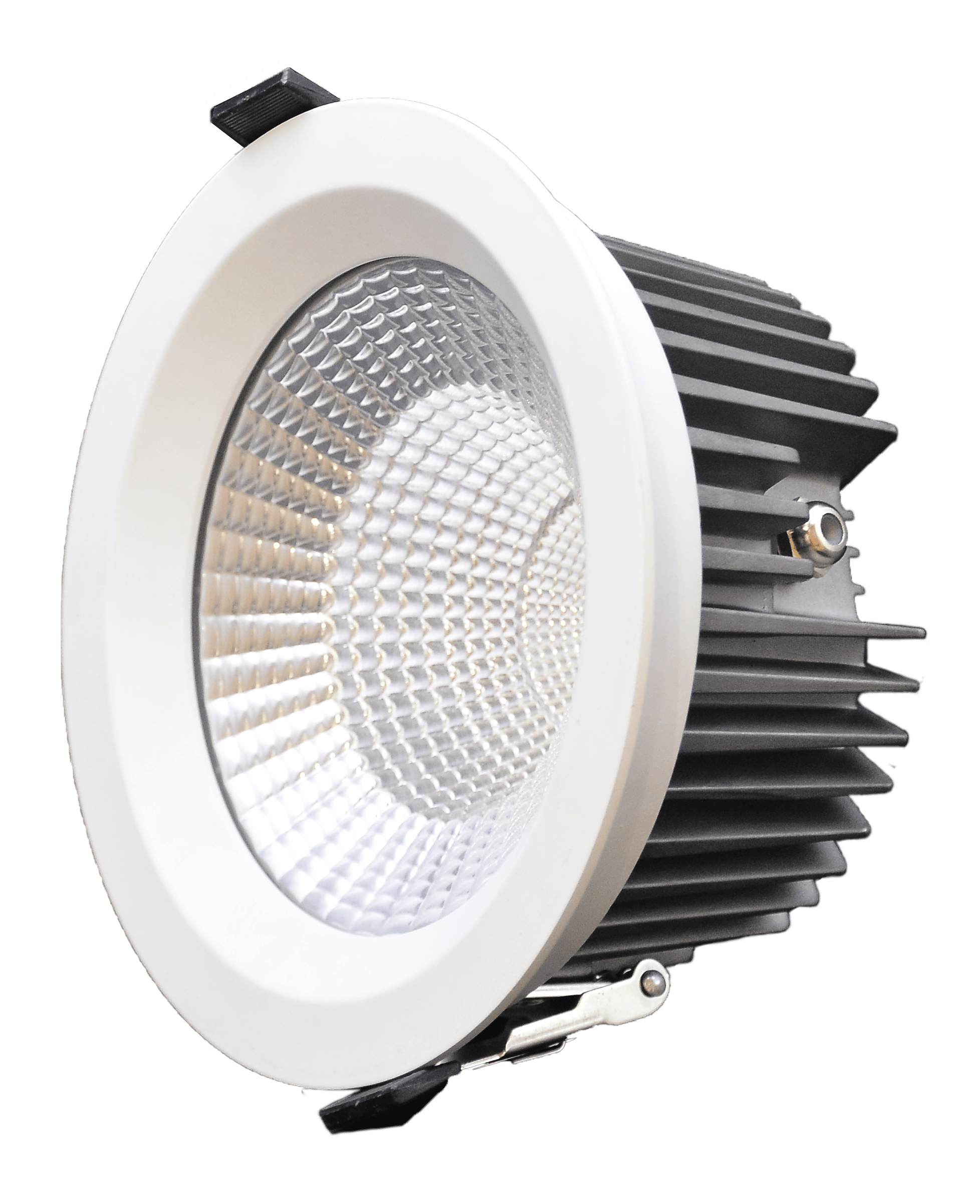
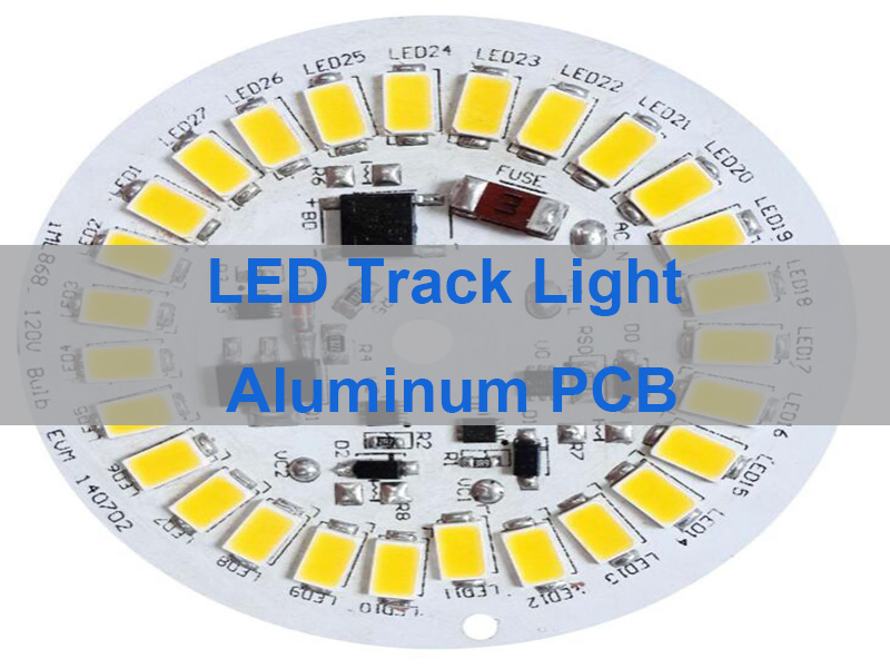
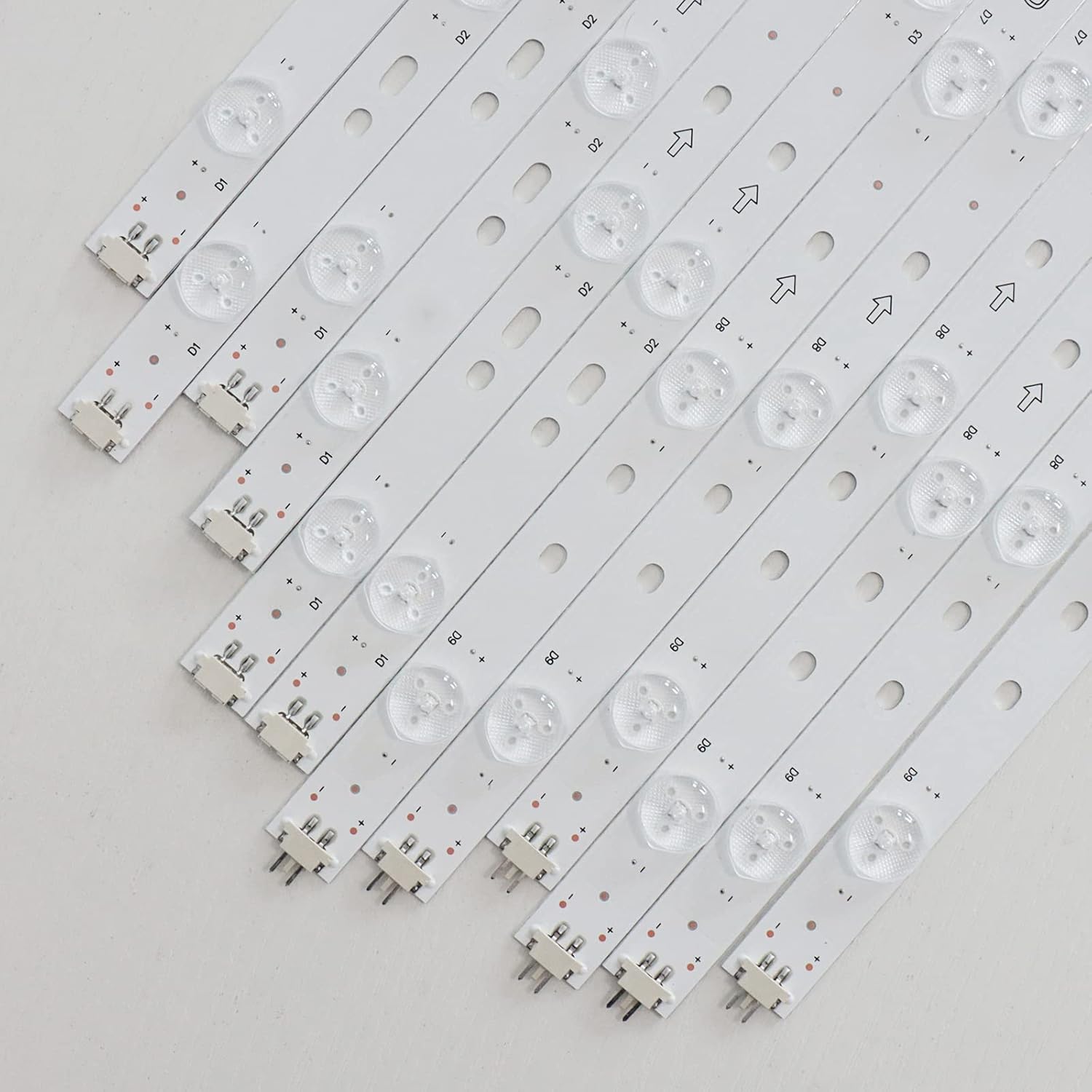
What Is LED Strip Light Aluminum PCB, and Why Is It Essential for LED Lighting?
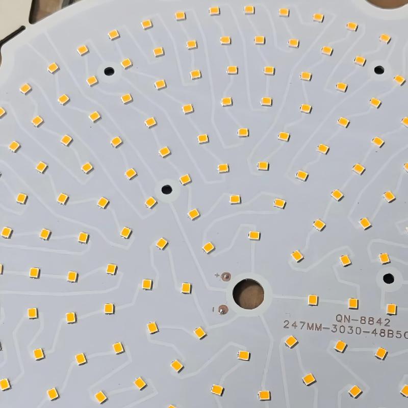
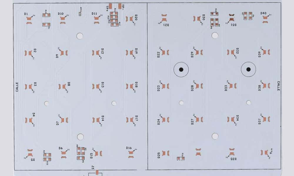
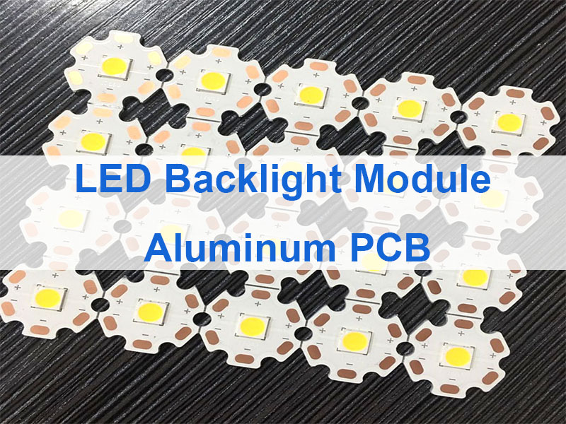
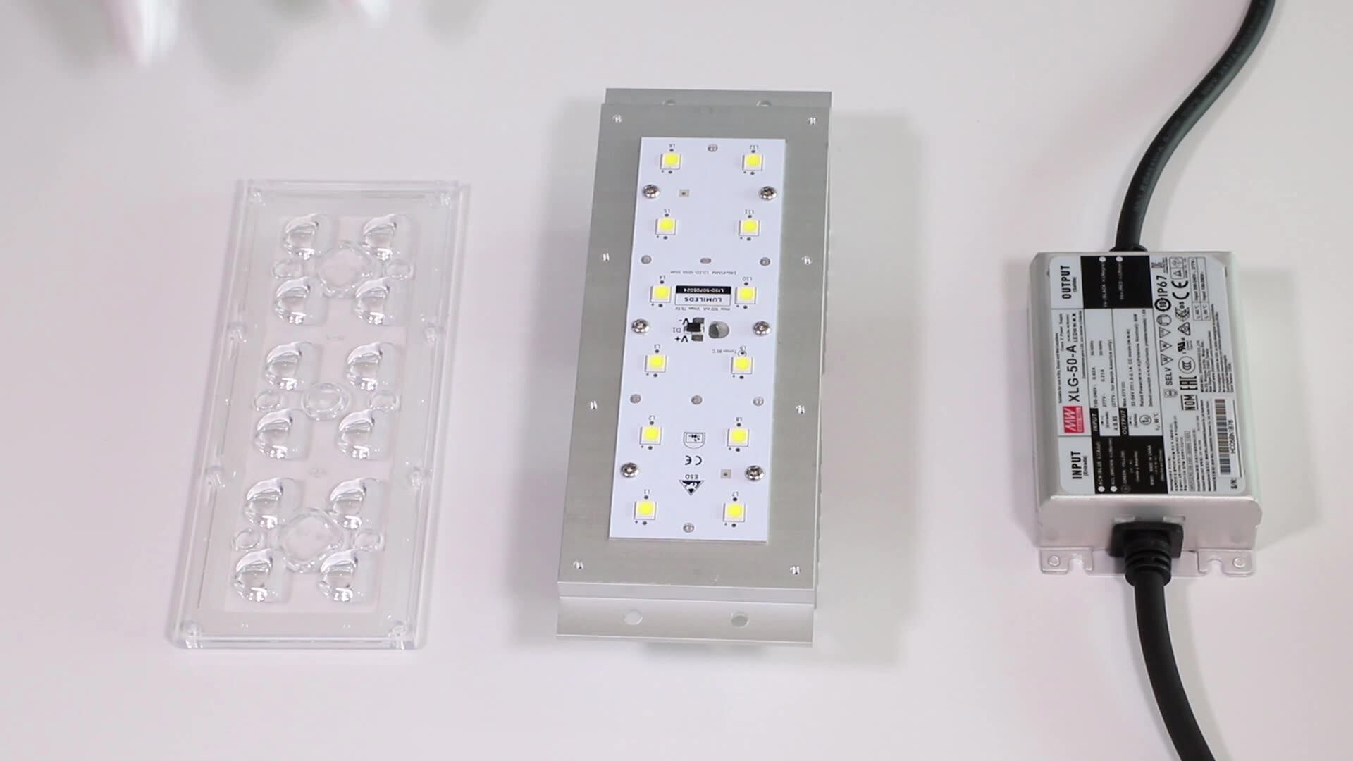
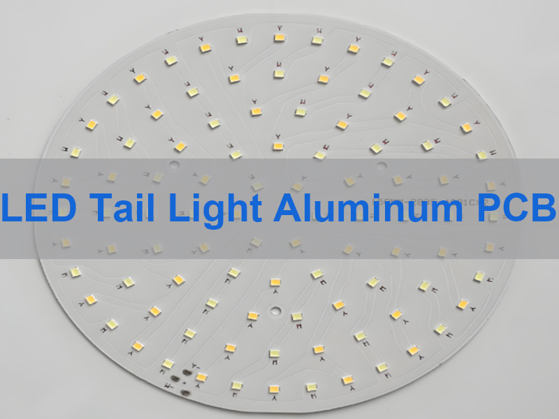
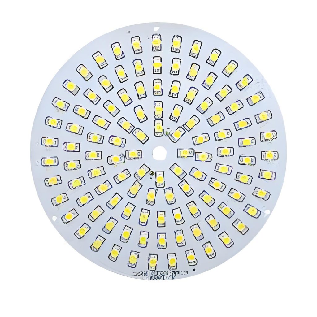
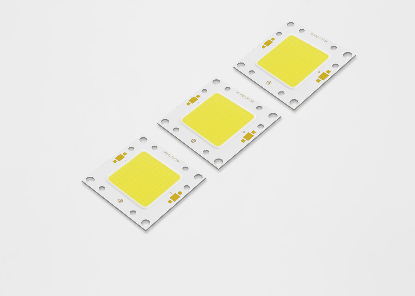
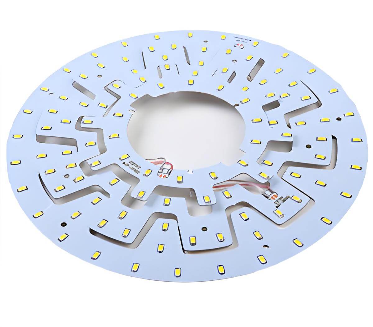
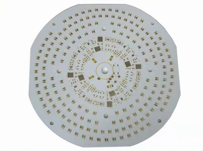
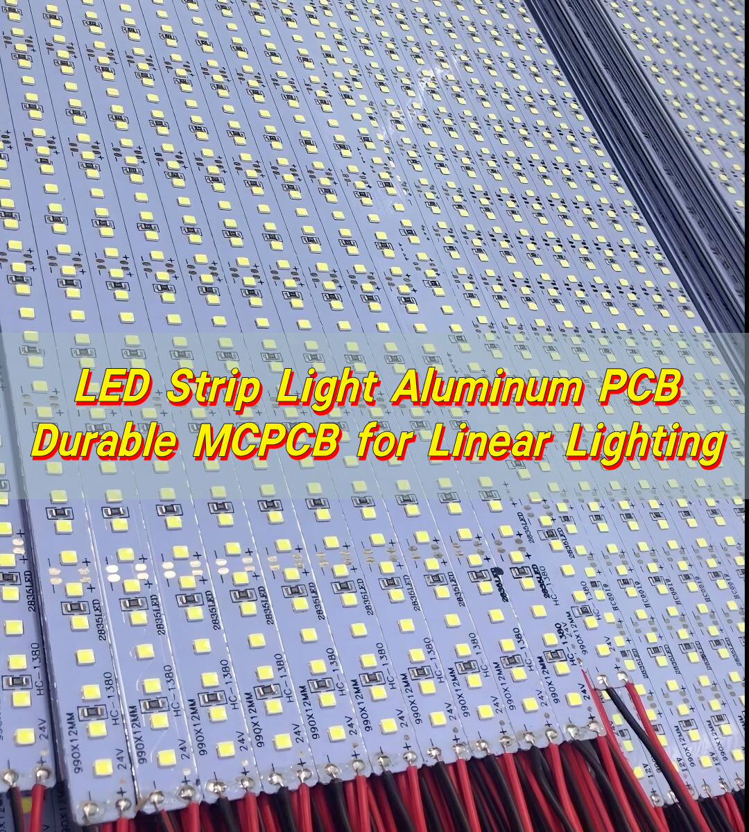
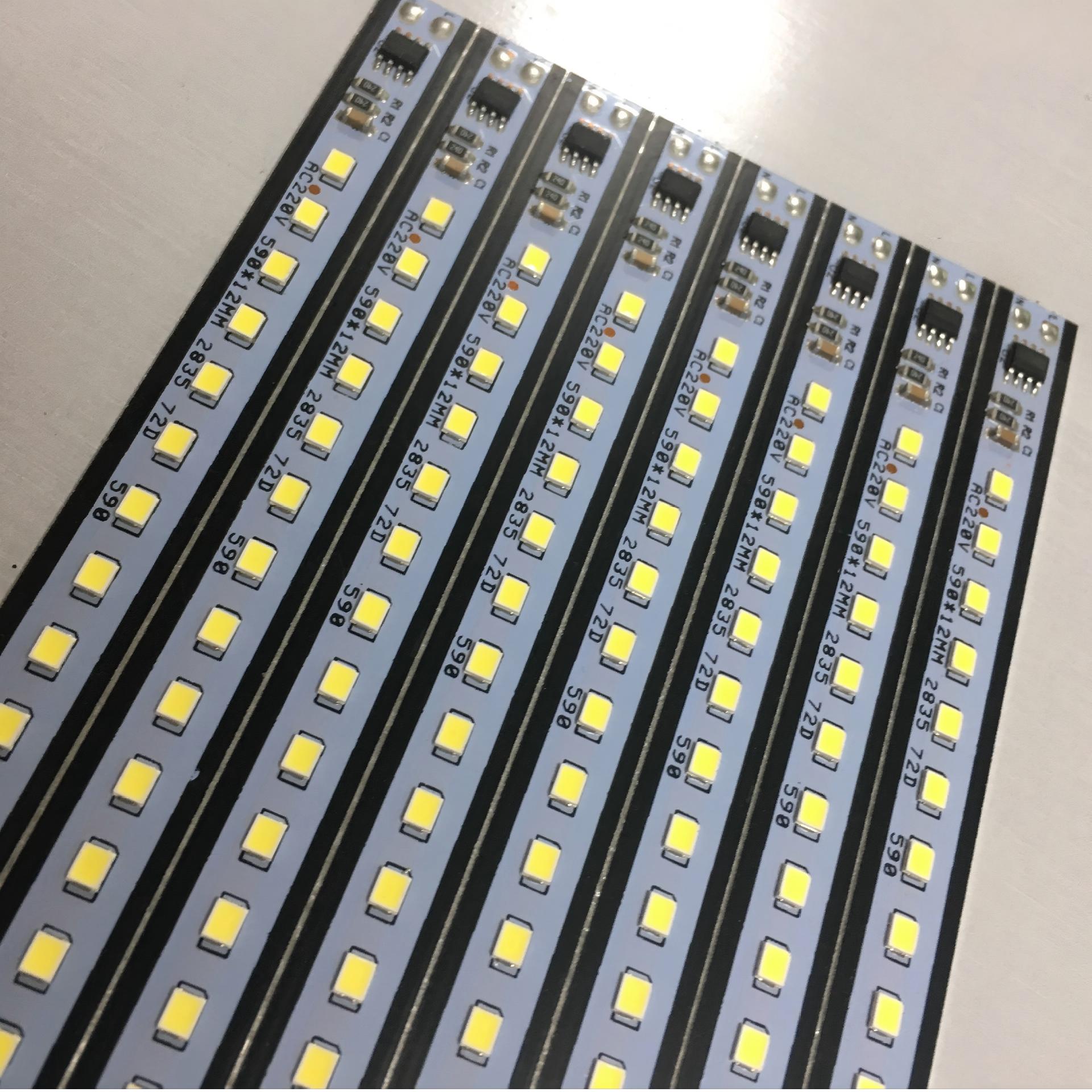
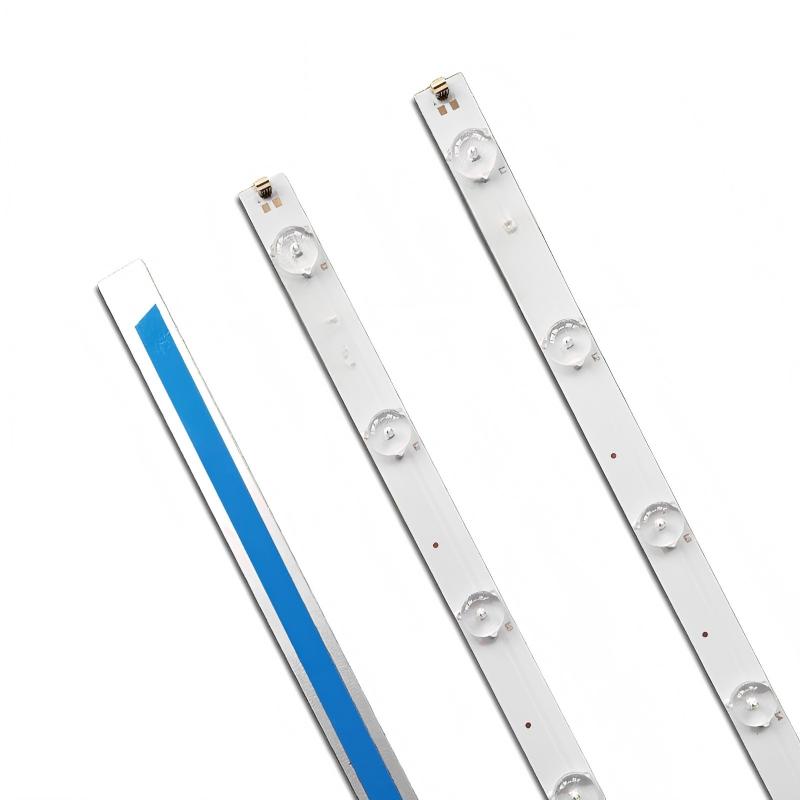
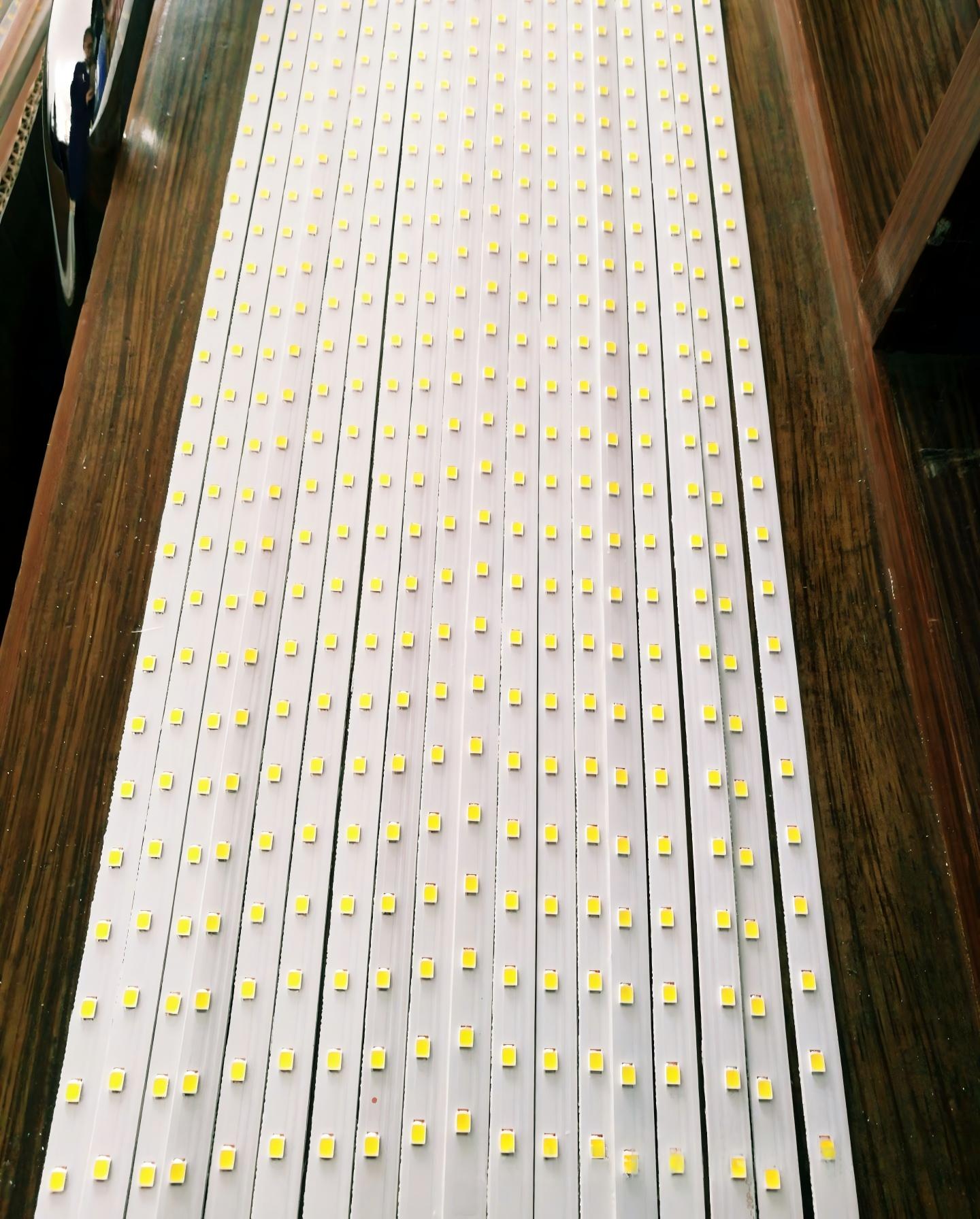
LED Strip Light Aluminum PCB is a specialized printed circuit board with an aluminum base, designed specifically for LED strip lights. It consists of three layers: circuit layer (copper foil), insulation layer, and metal base (aluminum).
It is essential for LED lighting because LEDs generate significant heat during operation—90% of electrical energy is converted to heat. Without proper heat dissipation, LED lifespan shortens by 50% for every 10℃ increase in junction temperature.
Our LED Strip Light Aluminum PCB efficiently transfers heat from LEDs to the aluminum base, reducing thermal resistance and extending LED lifespan by 300% compared to traditional FR-4 PCBs.
How to Design LED Strip Light Aluminum PCB for Optimal Heat Dissipation?
Optimal heat dissipation for LED Strip Light Aluminum PCB starts with three key design steps, ensuring heat is quickly transferred and dissipated to protect LEDs.
Key Design Tips for Heat Dissipation
- 1. Increase heat pad size: Extend the LED pad to a larger copper area to expand heat-carrying capacity, ensuring heat spreads evenly across the board.
- 2. Add sufficient thermal vias: Use 0.3mm vias spaced 1.5mm apart, with plugging and copper cladding to form a three-dimensional heat dissipation channel.
- 3. Choose appropriate copper thickness: For LEDs above 1W, use 2oz (70μm) copper foil to improve heat conduction and current-carrying capacity.
EBest’s design team can help you optimize your LED Strip Light Aluminum PCB layout for maximum heat dissipation, tailored to your specific project needs.
What Are the Differences Between LED Strip Light Aluminum PCB and FR-4 PCB?
LED Strip Light Aluminum PCB and FR-4 PCB differ significantly in heat dissipation, performance, and application. Below is a detailed comparison to help you choose the right option.
| Comparison Factor | LED Strip Light Aluminum PCB | FR-4 PCB |
|---|---|---|
| Thermal Conductivity | 1.0-3.0 W/(m·K), excellent heat dissipation | 0.2 W/(m·K), poor heat dissipation |
| LED Lifespan Impact | Extends LED lifespan by 300%+ | Shortens LED lifespan due to heat buildup |
| Mechanical Performance | High durability, resistant to bending and impact | Brittle, easy to crack under stress |
| Application | Ideal for LED strip lights, high-power LED lighting | Suitable for low-power electronics, non-heat-generating components |
| Temperature Resistance | -40℃ to 85℃, suitable for harsh environments | 0℃ to 60℃, limited to mild environments |
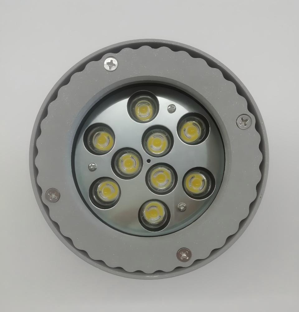
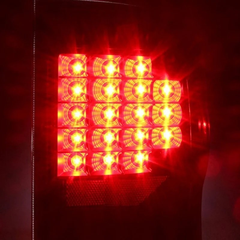
Which Industries Use LED Strip Light Aluminum PCB Most Frequently?
LED Strip Light Aluminum PCB is widely used in various industries that rely on high-performance LED lighting. Below are four popular industries and real application cases from EBest.
1. Residential Lighting Industry
Case: EBest provided LED Strip Light Aluminum PCB for a European residential lighting brand. The product featured 2oz copper foil and optimized heat dissipation design, ensuring stable light output for 50,000+ hours. It solved the client’s problem of frequent LED burnout in under-cabinet and ceiling strip lights.
2. Commercial Lighting Industry
Case: A shopping mall in the US partnered with EBest for LED strip lighting in its retail displays. Our LED Strip Light Aluminum PCB with anode oxidation treatment reduced light decay to 3% after 1000 hours of continuous use, meeting the mall’s high brightness and durability requirements.
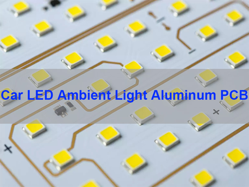
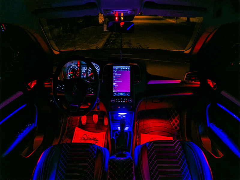
3. Automotive Lighting Industry
Case: EBest supplied LED Strip Light Aluminum PCB for automotive interior lighting (dashboard, door panels). The product met IATF 16949 standards, withstanding -40℃ to 85℃ temperature changes and ensuring stable performance in extreme driving conditions.
4. Outdoor Lighting Industry
Case: A highway tunnel project in Asia used EBest’s LED Strip Light Aluminum PCB for tunnel lighting. The product featured corrosion-resistant aluminum base and waterproof design, maintaining 88% light efficiency after 3 years of outdoor use.
How to Test the Quality of LED Strip Light Aluminum PCB?
Testing LED Strip Light Aluminum PCB quality is critical to avoid project failures. Follow these key steps to ensure your PCB meets industry standards and performance requirements.
Key Quality Testing Steps
- 1. Thermal Resistance Test: Use an infrared thermal imager to check surface temperature distribution. The temperature difference should not exceed 3℃ under 10W/cm² heat load.
- 2. Voltage Resistance Test: Verify the insulation layer can withstand 2kV+ breakdown voltage without leakage, ensuring electrical safety.
- 3. Circuit Continuity Test: Check for open circuits or short circuits in the PCB, ensuring all LED connections are stable.
- 4. Material Inspection: Confirm the aluminum base and copper foil meet specified grades, with no scratches, oxidation, or material defects.
EBest conducts all these tests on every batch of LED Strip Light Aluminum PCB, providing test reports for your peace of mind.
What Are the Latest Trends in LED Strip Light Aluminum PCB Technology?
The LED Strip Light Aluminum PCB industry is constantly evolving, with new technologies focusing on better performance, higher efficiency, and more sustainable designs.
- Trend 1: Higher thermal conductivity materials, such as ceramic-filled insulation layers, to further reduce thermal resistance and improve LED lifespan.
- Trend 2: Integrated design, combining LED driver circuits directly on the LED Strip Light Aluminum PCB to reduce product size and assembly complexity.
- Trend 3: Environmentally friendly materials and processes, ensuring all LED Strip Light Aluminum PCB products meet RoHS, REACH, and other green standards.
EBest stays ahead of these trends, investing in R&D to offer the latest LED Strip Light Aluminum PCB solutions for your projects.
How to Customize LED Strip Light Aluminum PCB for Your Specific Project?
Customizing LED Strip Light Aluminum PCB is simple with EBest, as we offer flexible solutions tailored to your project’s unique requirements. Follow these steps to get your custom PCB.
Customization Process
- 1. Share your requirements: Provide details like LED specifications, dimensions, thermal requirements, and application environment.
- 2. Design consultation: Our team will review your requirements and offer optimized design suggestions for your LED Strip Light Aluminum PCB.
- 3. Prototype production: We produce a small batch prototype for your testing, ensuring it meets your performance expectations.
- 4. Mass production: Once the prototype is approved, we start mass production with strict quality control and on-time delivery.
What Certifications Does EBest Have for LED Strip Light Aluminum PCB?
EBest holds multiple international certifications forLED Strip Light Aluminum PCB, ensuring our products meet global quality and safety standards. Below is a detailed list of our certifications.
| Certification Name | Scope of Application | Key Benefit |
|---|---|---|
| IATF 16949 | Automotive-grade LED Strip Light Aluminum PCB | Meets strict automotive industry quality standards |
| ISO 9001:2015 | All LED Strip Light Aluminum PCB products | Ensures consistent quality control processes |
| ISO 13485:2016 | Medical-related LED Strip Light Aluminum PCB | Complies with medical device quality requirements |
| AS9100D | Aerospace-grade LED Strip Light Aluminum PCB | Meets high-reliability aerospace standards |
| REACH | All LED Strip Light Aluminum PCB products | Complies with EU environmental regulations |
| RoHS | All LED Strip Light Aluminum PCB products | Free of hazardous substances |
| UL | All LED Strip Light Aluminum PCB products | Meets US safety standards for electrical products |
What Services Does EBest Offer for LED Strip Light Aluminum PCB?
EBest provides a full range of services for LED Strip Light Aluminum PCB, from design to delivery, ensuring a seamless experience for our clients.
Core Services
- 1. PCB Fabrication: Prototype and low-volume production of LED Strip Light Aluminum PCB, with custom substrate and material options.
- 2. Component Sourcing: Stable supply of all electronic components for LED Strip Light Aluminum PCB, including SMD, BGA, and QFN.
- 3. Assembly Services: Box Assembly, Through-Hole Assembly, and Flex PCB Assembly for complete LED strip solutions.
- 4. Value-Added Services: Injection molding, CNC Machining, and Sheet Metal services to support your entire product assembly.
- 5. Expedited Service: Urgent LED Strip Light Aluminum PCB orders can be shipped within 24 hours to meet your tight deadlines.
FAQ: Common Questions About LED Strip Light Aluminum PCB (Answered)
Below are the most common questions about LED Strip Light Aluminum PCB, with clear, concise answers to help you make informed decisions.
1. How long does LED Strip Light Aluminum PCB last?
LED Strip Light Aluminum PCB has a service life of 50,000+ hours when properly designed and manufactured. EBest’s products, with optimized heat dissipation, can extend this lifespan by an additional 20-30%.
2. Can LED Strip Light Aluminum PCB be used outdoors?
Yes, LED Strip Light Aluminum PCB can be used outdoors. EBest offers waterproof and corrosion-resistant options, with aluminum bases treated to withstand harsh weather conditions (-40℃ to 85℃).
3. What is the maximum current LED Strip Light Aluminum PCB can carry?
The maximum current depends on copper foil thickness: 1oz copper foil can carry up to 2A, 2oz up to 4A, and 10oz up to 15A. EBest can customize copper thickness based on your current requirements.
4. How to prevent LED color deviation with LED Strip Light Aluminum PCB?
Color deviation is prevented by using independent current-limiting resistors for each LED or color channel, and precision etching to ensure uniform current distribution. EBest’s design team optimizes PCB layout to eliminate color inconsistency.
5. Does LED Strip Light Aluminum PCB require a heatsink?
For low-power LED strips (≤10W), the aluminum base of the PCB acts as a sufficient heatsink. For high-power strips (>10W), EBest can integrate additional heatsink fins into the LED Strip Light Aluminum PCB design.
6. Can EBest produce flexible LED Strip Light Aluminum PCB?
Yes, EBest offers flexible LED Strip Light Aluminum PCB, combining the heat dissipation benefits of aluminum with the flexibility of flexible PCBs, ideal for curved or irregular lighting applications.
7. How long does it take to produce LED Strip Light Aluminum PCB?
Standard production time is 3-7 days for small to medium batches. EBest’s expedited service can deliver urgent orders within 24 hours, ensuring you meet your project deadlines.
How to Ensure Stable Supply of LED Strip Light Aluminum PCB for Mass Production?
Stable supply is critical for mass production of LED strip lights. EBest ensures consistent supply of LED Strip Light Aluminum PCB through three key measures.
First, we have long-term partnerships with trusted material suppliers, ensuring a steady supply of aluminum bases, copper foil, and insulation materials.
Second, our large production capacity (260,000 square feet/month) allows us to handle large orders without delays or supply gaps.
Third, we maintain safety stock of key materials for LED Strip Light Aluminum PCB, ensuring we can quickly respond to unexpected order increases or supply chain disruptions.
Why Is Thermal Management Critical for LED Strip Light Aluminum PCB?
Thermal management is critical for LED Strip Light Aluminum PCB because LEDs are highly sensitive to temperature. High temperatures cause LED light decay, color deviation, and premature failure.
LED chips convert 90% of electrical energy into heat. Without proper thermal management, junction temperatures rise, reducing LED lifespan by 50% for every 10℃ increase.
EBest’s LED Strip Light Aluminum PCB is designed to maximize heat dissipation, keeping junction temperatures below 70℃ and ensuring stable performance and long LED lifespan.
We provide high-quality LED Strip Light Aluminum PCB products and one-stop solutions to meet all your lighting project needs. Whether you need prototypes, custom designs, or mass production, EBest is your trusted partner. Contact us to place your order today at sales@bestpcbs.com