

Effective Pads PCB design is a cornerstone of creating reliable, high-performance printed circuit boards (PCBs). Pads serve as the critical connection points between components and the conductive traces of the board. This guide explores advanced concepts, materials, types, and design rules to optimize your PCB pad design for manufacturing (DFM) and long-term reliability.
Does poor pad design constantly undermine your PCB’s reliability and manufacturability?
- Frequent Solder Defects: Incorrect pad size or shape leads to tombstoning, bridging, or poor joints.
- Thermal Management Failure: Inefficient thermal pad design causes component overheating and reduced lifespan.
- Signal Integrity Issues: Poor pad-to-trace transitions create impedance discontinuities, degrading signal quality.
- Manufacturing Headaches: Pads incompatible with soldering processes cause low assembly yield and rework.
- Long-Term Reliability Risks: Weak pad connections fatigue and crack under thermal or mechanical stress.
Addressing these requires systematic design strategies focused on pad optimization.
- Precision Pad Geometry: Design pads per IPC standards and datasheets to ensure perfect solder fillets and joint strength.
- Optimized Thermal Management: Use via-in-pad with thermal simulation for effective heat dissipation from power components.
- Signal Integrity First: Apply controlled impedance design and smooth transitions at pads to maintain signal quality.
- DFM-Driven Design: Adhere to strict solder mask and stencil guidelines for flawless SMT assembly.
- Robustness Engineering: Reinforce connections with teardrops and robust pad structures verified by stress analysis.
EBest Circuit (Best Technology) offers a comprehensive range of solutions, including rigid PCBs, flexible circuits, rigid-flex circuits, metal-core PCBs, ceramic PCBs, PCB layout, and box-build assembly. Founded in 2006, we have specialized in one-stop PCB and PCBA services, covering PCB design, component sourcing, rapid prototyping, volume production, PCB assembly, and full box-build solutions. Our engineering and sales teams are professionally trained, with many members bringing over 10 years of hands-on project experience supporting global customers. We are certified to ISO 13485, AS9100D, and IATF 16949, and our production lines are integrated with an MES system to ensure traceability and process control. Our core focus markets include medical devices, aerospace, industrial control, and IoT applications, where reliability and compliance are critical. For factory audits or partnership inquiries, please contact us at sales@bestpcbs.com.
What Is Pads PCB Design?
Pads PCB design refers to the strategic planning, sizing, shaping, and placement of the conductive contact areas on a PCB where components are soldered. These circuit board pads are the fundamental interface for surface-mount (SMD) and through-hole components. The primary goal is to ensure a robust mechanical and electrical connection that can withstand assembly processes, thermal cycling, and operational stresses.
What Are PCB Pads Made Of?
PCB pads are fabricated from the same copper foil layer that forms the board’s traces. The process involves:
- Copper Foil: Typically Electrodeposited (ED) or Rolled Annealed (RA) copper, laminated onto the substrate.
- Surface Finish: A thin coating applied over the bare copper to prevent oxidation and enhance solderability. Common finishes include:
- HASL (Hot Air Solder Leveling): A traditional, cost-effective tin-lead or lead-free coating.
- ENIG (Electroless Nickel Immersion Gold): Provides a flat surface, excellent for fine-pitch components and gold wire bonding.
- OSP (Organic Solderability Preservative): A thin organic layer that protects copper until soldering.
- Immersion Silver/Tin: Offers good solderability and a relatively flat surface.
- Solder Mask: The polymer layer that covers most of the PCB but opens up at the pad locations to define the solderable area. Its proper alignment is critical.
What Are Design Pads For?
Pads serve multiple essential functions:
- Electrical Connection: Provide the conductive path for signals and power between the component and the PCB traces.
- Mechanical Anchor: Physically secure the component to the board.
- Thermal Path: Act as a channel to transfer heat from the component to the PCB planes or heatsinks, especially crucial for thermal pad PCB design.
- Soldering Interface: Define the area where solder forms the joint.
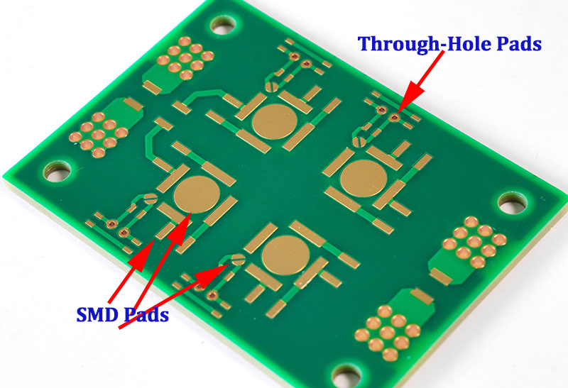
Types of PCB Pads and Their Applications
In PCB design, pads are more than simple solder points. Different pad types serve distinct electrical, mechanical, thermal, and manufacturing purposes. Understanding these differences helps engineers make faster, more reliable design decisions—especially when balancing assembly yield, testability, and long-term reliability.
| Pad Type | Description | Primary Application |
|---|---|---|
| Surface-Mount (SMD) Pads | Flat copper pads on PCB surface | Discrete SMDs, ICs, QFN, BGA |
| Through-Hole Pads | Copper annular ring around drilled hole | Connectors, power parts, DIP packages |
| Thermal Pads | Large central pad with heat paths | QFN, power ICs, heat dissipation |
| Test Pads | Exposed copper without components | ICT, flying probe testing |
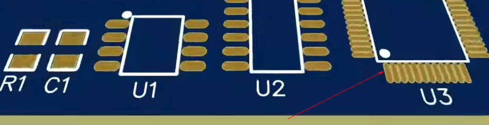
| Fiducial Pads | Non-solder reference pads | SMT alignment and vision systems |
| Solder Bridge Pads | Paired pads for optional shorting | Configuration, mode selection |
| Touch Pads | Copper pads for capacitive sensing | User interface controls |
While the table provides a quick reference, each pad type introduces specific design trade-offs that deserve attention during layout:
- SMD Pads: Pad geometry directly affects solder wetting, tombstoning risk, and placement accuracy. IPC footprint standards are often the starting point, but manufacturing capability must be considered.
- Through-Hole Pads: Hole diameter, annular ring width, and plating thickness determine mechanical strength and solder fill quality, especially in multi-layer boards.
- Thermal Pads: These pads strongly influence junction temperature and solder voiding behavior. Via patterns, paste coverage ratio, and reflow profiles must be coordinated, making thermal pad PCB design a cross-disciplinary task.
- Test Pads: Test accessibility is often overlooked until late in the project. Early planning improves coverage without increasing board size.
- Fiducial Pads: In PCB manufacturing, fiducial pads refer to optical fiducials realized as solid copper pads. Though electrically inactive, fiducials are critical for placement accuracy in high-density SMT assembly.
- Solder Bridge Pads: These enable low-cost configuration changes but require careful spacing to avoid unintended shorts during reflow.
- Touch Pads: Capacitive touch pads demand consistent copper geometry, controlled solder mask openings, and clean reference planes to ensure stable sensing.
In a nutshell, different PCB pad types exist because no single pad design fits every electrical, thermal, or manufacturing requirement. A well-chosen pad strategy improves assembly yield, testability, thermal performance, and overall product reliability.
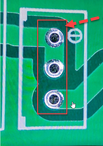
What Is Anti Pad in PCB Design?
An anti-pad is a clearance hole in an internal copper plane (power or ground) that electrically isolates a via or plated through-hole barrel from that plane. It prevents an unintended short circuit. The size of the anti-pad is a critical part of the PCB pad stack design and must be large enough to ensure proper insulation while maintaining plane integrity.
Difference Between Holes and Pads in PCB Design
This is a fundamental distinction in PCB pad hole design:
- Hole: A physical drilled cavity in the PCB. Its primary purposes are:
- To accommodate the lead of a through-hole component.
- To form the barrel of a via (for layer-to-layer connection).
- Pad: The copper land area that surrounds and connects to the hole. Its functions are:
- For Through-Hole Components: Provides the annular ring for soldering the lead and creating a reliable connection.
- For Vias: Can be a “tented” SMD pad on the surface or an internal connection point.
In short, the hole is the void; the pad is the conductive material around it that makes the connection possible.
Important Considerations for Pads PCB Design
Adhering to PCB pad design guidelines is essential for manufacturability and reliability.
- Pad Size & Shape (Land Pattern): Follow IPC-7351 standards. Pads must be large enough for a reliable solder fillet but not so large as to cause bridging or tombstoning.
- Solder Mask Definition: The solder mask opening should be slightly larger than the copper pad (typically 0.05-0.1mm per side) to prevent misalignment from exposing the trace.
- Silkscreen Clearance: Silkscreen PCB design guidelines mandate that ink must never cover a pad. Maintain a minimum clearance (e.g., 0.2mm) to avoid contamination.
- Copper-to-Edge Clearance: Pads, especially for connectors, must be set back sufficiently from the board outline to prevent shorting during routing.
- Trace Connection: Use teardrops where PCB design trace between pads or traces connect to small pads/vias to strengthen the joint and prevent cracking.
- Thermal Relief Pads: Use for connections to large copper planes (like ground) to prevent heat sinking, which makes soldering difficult.
Thermal Pad Design and Solder Voiding
Thermal pad PCB design for components like QFNs is critical. A central pad with a grid of small vias (“via-in-pad”) is used for heat dissipation. However, this can lead to solder voiding as gases escape during reflow. Mitigation strategies include:
- Via-in-Pad Design: Use small diameter vias (e.g., 0.2mm) and ensure they are filled and capped (with epoxy or copper) to prevent solder wicking into the via and creating voids.
- Solder Paste Stenciling: Use a segmented stencil opening (grid of small apertures) over the thermal pad instead of one large opening to allow gases to escape.
- Optimized Reflow Profile: A slower temperature ramp can help gases escape before the solder seals the area.
Via-in-Pad Techniques and Design Trade-Offs
PCB design via in pad places vias directly in the SMD pad, offering significant benefits but requiring careful management.
- Advantages:
- Space Savings: Eliminates the need to route traces away from the pad to access a via.
- Improved Electrical Performance: Provides the shortest possible path for high-speed or power signals, reducing inductance.
- Enhanced Thermal Conductivity: Critical for thermal modeling and design optimization of PCB vias and pads under BGAs and QFNs.
- Trade-Offs and Solutions:
- Solder Wicking/Voiding: Solder can flow down the via barrel, starving the joint. Solution: Specify filled and plated-over (capped) vias.
- Increased Cost: Via filling and capping adds process steps and cost.
- Assembly Complexity: May require sequential lamination or specialized processes.
A related but distinct practice is PCB design vias on pads for through-hole components, where vias are placed adjacent to the component hole’s pad to route signals to other layers, which is generally more straightforward.
FAQs
Q: What Is the Difference Between a Pad and a Via?
A: A pad is primarily designed to make a connection to a component lead. A via is a plated through-hole designed solely to provide an electrical connection between different layers of the PCB. A via can be placed within a pad (via-in-pad) or connected to it by a short trace.
Q: What Is the Difference Between a Pad and a Lead?
A: The pad is the copper feature on the PCB. The lead (or pin) is the metallic terminal of the electronic component that is soldered to the pad.
Q: What Are the Key Elements of Pad Design?
A: The key elements are defined in the PCB pad stack design and include:
- Copper Layer Geometry: Size, shape, and orientation of the pad on each relevant layer.
- Solder Mask Opening: Size and alignment relative to the copper.
- Paste Mask Layer (for SMD): Defines the stencil aperture for solder paste.
- Drill Information (for through-hole): Hole size and location.
- Anti-pad Size (for planes): Clearance in internal copper layers. By mastering these elements, you ensure your PCB design pads form the foundation of a robust and reliable circuit assembly.
Q: Are Fiducial Pads the Same as PCB Fiducial Markers?
A: Yes. In PCB engineering and SMT assembly, fiducial pads and PCB fiducial markers refer to the same functional feature.
Both describe exposed copper reference points used by pick-and-place machines, AOI systems, and other automated assembly equipment to accurately locate and align the PCB during component placement.
The term PCB fiducial markers is the industry-standard expression commonly used in SMT process documentation and equipment manuals, while fiducial pads emphasizes the physical pad structure on the PCB itself. In practice, the two terms are interchangeable, and the difference is mainly one of wording rather than function.