

What is small PCB board? Let’s explore its definition, benefits, applications, design spec and guide, production process and recommended PCB manufacturer through this blog.
Are you troubled with these problems?
- How to fit multi-modules (sensors + 5G) in wearables without compromising performance?
- How to ensure stable signals for 5G/AR modules with micro-scale traces?
- How to prevent thermal failure in compact devices like drones/medical portables?
As a professional small PCB manufacturer, we can provide you service and solutions:
- Space Optimization: Micron-scale HDI routing and 4-layer stackup integrate controller, sensor, and Bluetooth within 20cm² with 40% density improvement.
- Signal Stability: Routing simulation and arc transitions reduce 5G module delay by 20% and crosstalk by 15dB.
- Thermal Control: High-density thermal vias and heat channels limit temperature rise to ≤30°C with 25% efficiency gain.
- Compact PCB challenges solved with three key solutions precise routing, stable signals, optimized thermal management.
Welcome to contact us if you have any request for small PCB board: sales@bestpcbs.com.
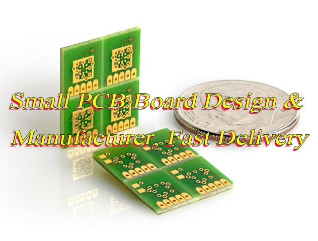
What is Small PCB Board?
Small PCB Board refers to a printed circuit board designed with significantly reduced physical dimensions (typically under 20 cm² in area or with any side ≤50 mm) to fit space-constrained applications, while integrating essential electronic components and conductive pathways to enable specific functionalities within compact devices like wearables, medical implants, or micro-sensors. Its miniaturization necessitates specialized manufacturing techniques, such as high-density interconnect (HDI), laser micro-vias, and precise impedance control to maintain electrical performance despite stringent size limitations.
What Are Benefits of Small Circuit Board?
Space Utilization Optimization
- Minimize equipment size to meet rigid compact layout requirements for wearables/IoT modules.
- Multi-layer stack design enables complex functions within limited area, reducing overall system footprint.
Signal Integrity Enhancement
- Shortened trace length reduces signal delay/crosstalk, ideal for high-frequency circuits (e.g., 5G/RF modules).
- Ground/power planes facilitate low-impedance design, mitigating EMI risks.
Cost Control Superiority
- Reduced material consumption (substrate/copper foil) directly lowers per-unit production costs.
- Smaller boards optimize panelization efficiency in mass manufacturing.
Thermal Performance Improvement
- Concentrated layout enables targeted thermal management (e.g., localized thermal vias/conduits).
- Shortened thermal resistance paths enhance heat dissipation efficiency for high-power components (e.g., ICs).
Lightweight Design Support
- Reduces end-product weight, critical for drones/medical portables.
- Compatible with flexible PCBs for 3D space-saving installation.
Production Yield Improvement
- Smaller area reduces warpage risk during soldering processes (e.g., wave soldering).
- Higher AOI inspection/repair efficiency due to accessible defect locations.
Iteration Flexibility Enhancement
- Lower cost for rapid prototyping (e.g., quick-turn PCB samples) accelerates product validation cycles.
- Modular design supports incremental upgrades without full system redesign.
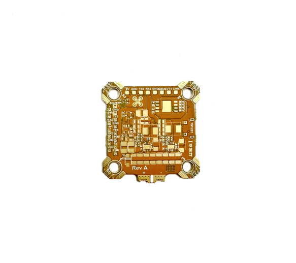
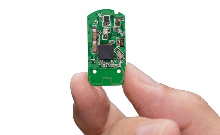
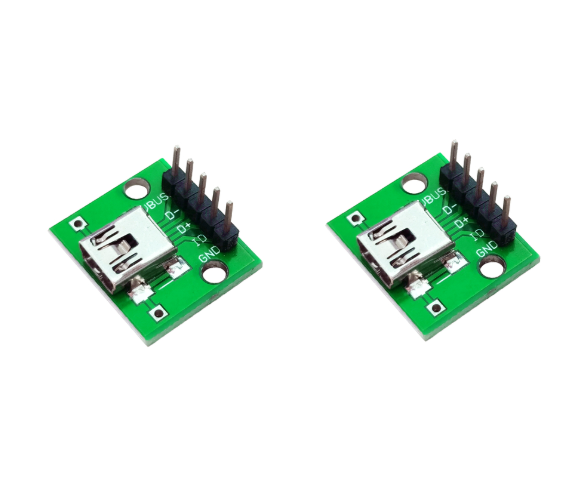
What Are Applications of Small PCB Board?
- Consumer Electronics: Smartwatch/bracelet main control boards, TWS earphone circuits, smartphone camera modules.
- Medical Devices: Cardiac pacemaker control boards, endoscopic imaging modules, portable glucose meter sensor circuits.
- Industrial Automation: Micro-sensors (temperature/humidity/pressure), PLC interface modules, instrumentation control cores.
- IoT (Internet of Things): Smart home sensor nodes, RFID tags, environmental monitoring terminals.
- Automotive Electronics: ADAS radar control units, in-vehicle infotainment micro-modules, tire pressure monitoring chips.
- Aerospace: Drone flight control boards, satellite attitude adjustment circuits, spacecraft micro-sensors.
- Communication Equipment: 5G micro-base station RF modules, fiber optic transceiver core boards, millimeter-wave antenna arrays.
- Advanced Technology: AR/VR glasses driver boards, nanorobot control units, bionic mechanical power systems.
- Education & Research: Experimental teaching microcontrollers, scientific research detection device circuits, micro-prototype development boards.
Small PCB Board Design Technical Parameter
| Specific Parameter | Value/Range |
| Minimum trace width | 6mil (0.153mm) |
| Standard design trace width | 10mil (0.254mm) |
| Minimum trace spacing | 6mil (0.153mm) |
| Trace to board edge clearance | 0.508mm (20mil) |
| Minimum via hole size | 0.3mm (12mil) |
| Via spacing | ≥6mil (Recommended 8mil) |
| PTH hole size design | ≥Component pin +0.2mm |
| PTH pad outer ring | ≥0.2mm (8mil) |
| Hole size to board thickness ratio | ≤5-8 |
| 1OZ copper thickness | ≈35μm |
| 2OZ copper thickness | ≈70μm |
| Solder mask opening single-side | 0.1mm (4mil) |
| Character width | ≥0.153mm (6mil) |
| Character height | ≥0.811mm (32mil) |
| Slot design minimum spacing | ≥1.6mm |
| Panelization gap | ≥1.6mm (For 1.6mm board thickness) |
| Panelization process edge | ≥5mm |
| Power trace width recommendation | 50-100mil |
| Signal trace width recommendation | 8-12mil |
| Ground plane priority | Widest |
Small PCB Board Design Guideline
Below is a guide of small PCB board design:
1. Precision Dimension Control & Tolerance Verification
- Outline Size Standards: Strict adherence to ≤20cm² limits (e.g., 10mm×10mm smartwatch mainboards) with 0.1-1.2mm ultra-thin substrates (FR4-Tg170+), validated by IPC-2221 ±0.1mm tolerance. Case: Medical implants achieve seamless tissue integration via 0.2mm tolerance control.
- 3D Space Optimization: MCAD tools (SolidWorks) ensure ≥0.5mm clearance between PCB/housing/batteries, preventing assembly stress-induced cracks.
2. Stackup Optimization & Simulation Validation
- Stackup Strategy: 4-layer “Signal-GND-Power-Signal” reduces HF crosstalk by 40% (5G module validation data); 8-layer expands to “Signal-GND-Signal-Power-GND-Signal-GND-Signal” for multi-channel radar units.
- HDI Microvia Application: 0.1mm/0.08mm trace/space via laser-drilled 0.1mm microvias, paired with blind/buried vias to enhance routing density. Example: AR glasses driver boards achieve 3× density increase and 20% latency reduction via HDI.
3. Impedance & Signal Integrity Refinement
- Control Standards: 50Ω±10%@900MHz (TDR error ≤5%), differential 100Ω±5%; length matching ≤5mil (0.127mm) prevents timing skew. Case: UHF RFID read range improved by 30% via impedance tuning.
- EMI/Crosstalk Mitigation: 135° arc transitions replace 90° bends; SIwave simulations ensure ≤10mV ground bounce. Real-world: Automotive infotainment EMI reduced by 15dB via optimized grounding.
4. Thermal Management Strategies & Thermal Simulation
- Via Design: ≥10/cm² density, 0.2-0.3mm diameter, ≥3W/m·K conductivity (Cu-graphene composites); 0.5mm copper thermal channels paired with FloTHERM simulations limit ΔT≤30℃. For example: Drone flight controllers reduce IGBT ΔT by 25℃.
- Thermal-Mechanical Coupling: ANSYS Mechanical validates CTE matching, preventing delamination. Industrial sensors achieve 2× reliability improvement via coupled analysis.
5. Power Integrity Deep Design & Verification
- Plane Segmentation: ≤0.5mV noise (PI simulation validated), decoupling caps ≤5mm (0402 packages); dedicated power layers with low-ESR caps (10μF/6.3V) minimize ripple. Case: 5G microbase stations achieve 12dB noise reduction.
- PDN Analysis: SIwave ensures ≤5% voltage drop for high-speed digital circuits.
6. Material & Surface Finish Selection
- Substrates: PTFE (εr=2.1)/ceramic (εr=9.8) for mmWave; FR4-Tg170+ for general use. Copper thickness: 18μm inner/35μm outer layers.
- Finishes: ENIG for reliability, OSP for cost efficiency; Immersion Ag for HF applications.
7. DFM Full-Process Compliance
- Drilling: Laser-drilled 0.1mm (HDI), mechanical 0.2mm; V-cut/stamp hole panelization for SMT (0201 components).
- DFM Checks: Mentor tools validate min holes/trace/spacing; ≥2mm test point spacing and full AOI coverage ensure ≥99% yield (CPK≥1.33).
8. Mechanical & Reliability Full-Spectrum Validation
- Mounting Holes: ±0.1mm tolerance, IEC 60068-2-27 shock test (500g/1ms); -40℃~125℃ range with 85℃/85%RH/1000h and -55℃~125℃/500-cycle tests.
- Certifications: ISO 13485 (medical), AEC-Q100 Grade 1 (automotive), IEC 60947 (industrial). Example: ADAS modules achieve decade-long fault-free operation via AEC-Q100.
How to Make a Small Printed Circuit Board?
1. Circuit Design and File Generation
- Using EDA software (e.g., Altium Designer 23, KiCad) to complete schematic design and PCB layout, generating Gerber files containing circuit, drilling, and solder mask information. DFM review ensures compliance with IPC-A-600 standards, including minimum trace width (6mil/0.153mm), spacing (8mil/0.2mm), and hole size tolerance (±0.05mm).
2. Substrate Preparation and Cutting
- Select FR-4 epoxy glass cloth substrate (IPC-4101 certified) based on application requirements. Cut large copper-clad laminate to design size using precision shearing machines. Perform mechanical/chemical cleaning (e.g., pumice scrubbing) to remove oxidation and ensure surface adhesion for subsequent processes.
3. Inner Layer Circuit Formation
- Apply dry film photoresist on copper-clad board, transfer design patterns via UV exposure (365nm wavelength, 10-20mJ/cm? energy). Develop to remove unexposed areas, etch unprotected copper using ferric chloride solution, then strip residual film. AOI inspection detects defects like shorts/opens with 5μm resolution.
4. Lamination and Stacking
- After browning treatment (copper surface oxidation to enhance bonding), alternate core boards and prepreg (PP) sheets. Stack with copper foil outer layers, press under vacuum/hot-press (180-200℃, 300-500psi pressure) to achieve layer bonding and curing. Semi-cured epoxy resin forms insulated interlayer connections.
5. Drilling and Hole Metallization
- Mechanical/laser drilling creates through-holes/blind vias (diameter down to 0.1mm). Hole wall metallization involves chemical copper deposition (0.3-1μm thin layer) followed by electroplating to 20-25μm thickness. X-ray drilling ensures positional accuracy ±0.05mm.
6. Outer Layer Circuit Formation
- Repeat inner-layer process: apply liquid photoresist → exposure → pattern plating (copper/tin) → etching → stripping. Differential etching ensures uniform copper thickness. Tin protection preserves circuit patterns during etching.
7. Solder Mask and Surface Finish
- Apply epoxy ink (e.g., green solder mask) via screen printing, expose/develop to open pad windows. Surface finishes include HASL (tin/lead), ENIG (immersion gold), or OSP (organic solderability preservative) to enhance solderability and corrosion resistance.
8. Silkscreen and Profiling
- Screen-print component markings/logos using UV-curable ink (≥6mil/0.153mm line width). Profile cutting via CNC routing or V-scoring (depth control ±0.1mm) ensures panel separation with smooth edges.
9. Electrical Testing and Inspection
- Conduct continuity/insulation testing using flying probe/ICT fixtures. AOI/AXI detects defects like missing pads/solder bridges. Final checks include dimensional verification (calipers/CMM), impedance testing (±10% tolerance), and thermal shock testing per IPC-TM-650.
10. Packaging and Shipping
- After ultrasonic cleaning and baking, boards undergo vacuum packaging with desiccant and humidity indicator cards. Labels include batch number, production date, and QA certification. Ships in ESD-safe containers compliant with RoHS/REACH standards.
Why Choose EBest Circuit (Best Technology) as Small PCB Board Manufacturer?
Reasons why choose us as small PCB board manufacturer:
- Cost Optimization Solution: By optimizing material selection and process pathways, we reduce production costs for small and medium batch orders by 12%-18%. Combined with a dynamic cost accounting system, we deliver cost-sensitive design solutions for clients. This has helped over 300 customers achieve an average annual manufacturing cost savings of 15%.
- Rapid Prototyping System: Urgent orders support 24-hour rapid prototyping. Leveraging dual-shift production lines and intelligent scheduling systems, we compress the industry-average 48-hour prototyping cycle by 50%. 2024 data shows over 85% of expedited orders complete prototype verification on the same day, accelerating product iteration efficiency.
- On-Time Delivery Guarantee: 99.2% on-time delivery rate, verified by ISO 22483 supply chain management certification, significantly outperforms the industry average of 95%. Through AI-driven production forecasting and dynamic inventory allocation, Q3 2025 data indicates over 98% of orders are delivered ahead of schedule or on time, enhancing client supply chain stability by 40%.
- Full-Inspection Quality Control: Batch orders undergo 100% full inspection using AOI and X-ray dual inspection systems, achieving a defect detection rate of 99.2%. Compared to manual sampling, efficiency improves by 300%. 2024 customer return rates remain below 0.03%, far below the industry average of 0.5%.
- Authoritative Certification System: Certifications include ISO 9001:2015, IATF 16949:2016 automotive-grade, medical ISO 13485, and RoHS 2.0 lead-free compliance. Covering high-compliance sectors like automotive electronics, medical devices, and industrial control, we added EU CE-RED wireless device certification in 2025 to meet global market access requirements.
- Experience-Based Knowledge System: Built on 19 years of PCB production data, our error database contains over 200,000 process defect cases and solutions. AI-driven analysis identifies 85% of design risks in advance, reducing client trial-stage problem-solving time by 40% and minimizing repeated trial costs.
- Free DFM Analysis: Complimentary Design for Manufacturability (DFM) analysis combines EDA tools with engineering expertise to identify design flaws like trace width/spacing violations and impedance mismatches early. 2024 data shows DFM reduces client design revisions by 45% and shortens product launch cycles by an average of 21 days.
- End-to-End Service Chain: Integrating design consulting, prototyping, SMT assembly, functional testing, and logistics through an ERP system for real-time order tracking. Clients reduce supply chain management costs by 25% and improve coordination efficiency by 30%, ideal for multi-SKU small-batch orders.
Welcome to contact us if you have any inquiry for small PCB board: sales@bestpcbs.com.