What is one sided copper PCB? Let’s discover its features, pros and cons, application, technical parameter, design guide, production processes.
Are you troubled with these problems?
- Poor heat dissipation in single-sided PCBs leads to deformation at high temperatures and shortens equipment lifespan.
- With limited budgets, is it impossible to balance copper layer thickness, substrate materials, cost, and performance?
- Are long prototyping cycles and slow mass production deliveries delaying your R&D progress?
As a copper PCB manufacturer, EBest Circuit (Best Technology) can provide you service and solutions:
- Metal Substrate + Optimized Single-Sided Copper: Aluminum/copper base improves heat dissipation by 300%, prevents deformation at high temperatures, and extends lifespan by over 30%.
- Customizable Thickness + Tiered Pricing: Flexible selection of 1oz to 3oz copper layers meets industrial needs at 15% lower costs than competitors.
- 24-Hour Rapid Prototyping + 15-Day Mass Production: Direct supply from our own factory, end-to-end tracking of urgent orders, and daily compensation for delays.
Welcome to contact us if you have any inquiry for one sided copper PCB board: sales@bestpcbs.com.
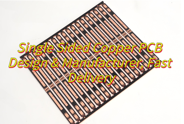
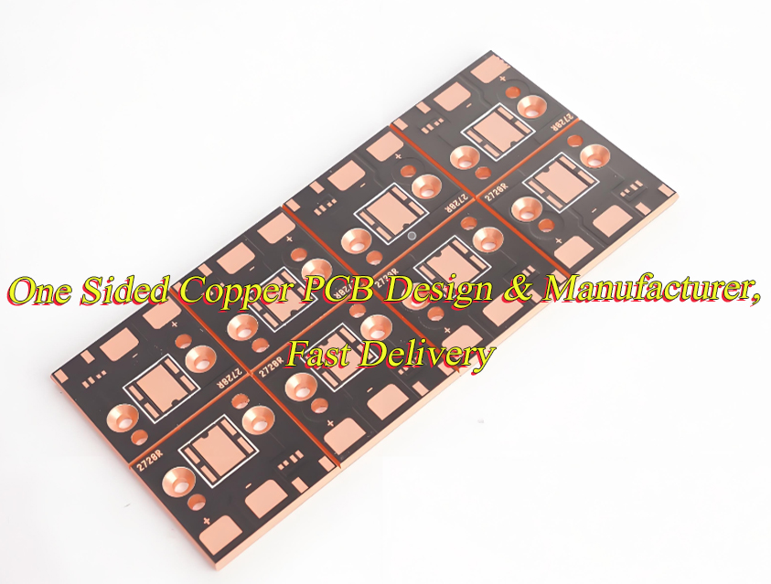
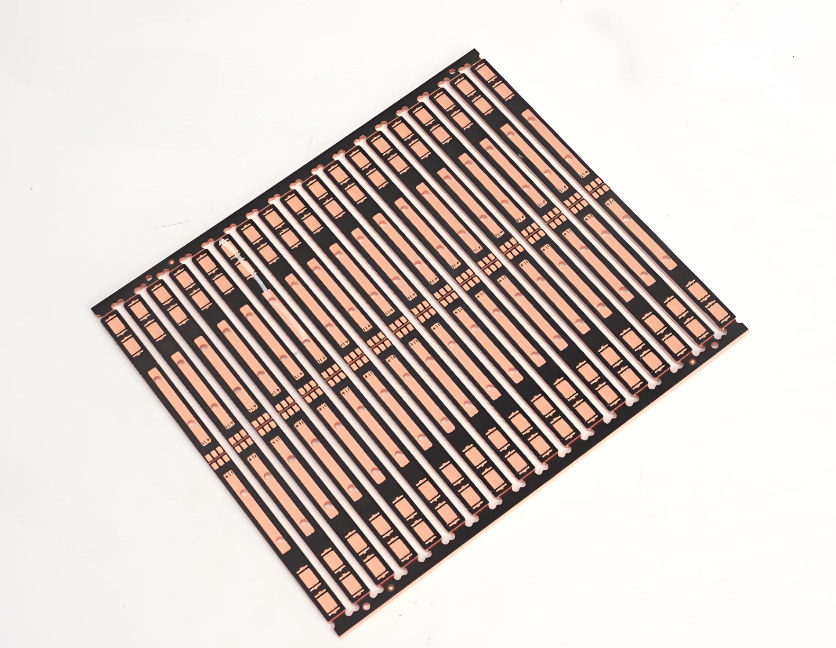
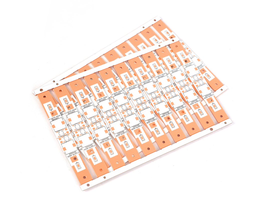
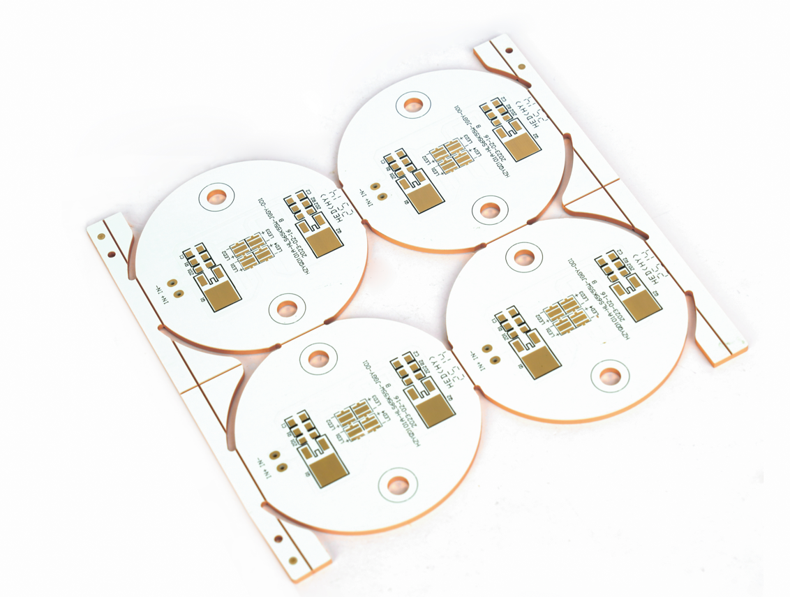
What Is One Sided Copper PCB?
A One Sided Copper PCB ( also called as single sided copper PCB) is a printed circuit board (PCB) that has a single layer of copper foil as a conductive layer covered only on one side of an insulating substrate (such as epoxy resin or fiberglass). Its structure consists of a substrate, a single layer of copper foil conductive layer, a solder mask layer (to prevent solder bridging short circuits), and a silk screen layer (to identify component positions and parameters).
Because it only has single-sided wiring capabilities, it is suitable for electronic devices with low circuit density and simple functions (such as calculators and LED light boards). It has the advantages of low cost, simple manufacturing process, and high heat dissipation efficiency.
What Are Features of One Sided Copper PCB?
- Minimalist structure: Single copper layer on one side of insulating substrate (e.g., FR-4, polyimide), with solder mask and silkscreen for protection/labeling.
- Cost efficiency: Low material/manufacturing costs, ideal for mass production of low-complexity devices (e.g., calculators, LED strips).
- Manufacturing simplicity: Standardized processes (lithography, etching) enable high yield, fast prototyping, and easy quality control.
- Low-complexity focus: Optimized for low-frequency, low-power circuits (e.g., power modules, sensors, basic controls).
- Thermal-electrical balance: Copper’s high thermal conductivity (∼400 W/m·K) supports heat dissipation in LED drivers/small motor controls.
- Mechanical versatility: Rigid FR-4 for vibration resistance; flexible substrates (e.g., polyimide) for bendable/compact designs.
- Surface treatment options: HASL, ENIG, OSP for solderability/anti-oxidation, adapting to through-hole/SMT and lead-free requirements.
- Eco-friendly design: RoHS-compliant materials and recyclable copper align with sustainable manufacturing trends.
What Are Pros and Cons of Single Sided Copper PCB Board?
Pros of Single-Sided Copper PCB
- Cost Efficiency: Material and production costs are 30%-50% lower than multi-layer boards, making it ideal for mass-produced items like remote controls, LED panels, and basic home appliances.
- Design Simplicity: Single-layer routing eliminates complex inter-layer alignment and via design, reducing errors. Customizable copper thickness (1-20 oz) suits low-current needs, while robust substrates (e.g., FR-4) withstand extreme temperatures (-50°C~300°C) and vibrations.
- Thermal Performance: Direct heat conduction via the copper layer, enhanced by aluminum/ceramic substrates, prevents overheating in high-current applications (e.g., motor controllers, LED drivers).
- Lightweight & Compact: Thickness (0.8-3.2mm) and weight (20%-40% lighter than multi-layer boards) benefit portable devices like electronic scales and IoT sensors.
- Rapid Prototyping & Maintenance: 24-48 hour sample production, straightforward AOI/X-ray inspection, and easy repairs suit educational projects, DIY kits, and quick design iterations.
- Eco-Friendly Customization: Halogen-free substrates meet EU standards; specialized materials (e.g., ceramic) improve durability in harsh environments (e.g., outdoor solar lighting).
Cons of Single-Sided Copper PCB
- Limited Wiring Density: Minimum trace width/spacing (≥0.3mm) restricts high-density circuits (e.g., 5G modules, advanced processors), requiring multi-layer boards for complex designs.
- EMI Vulnerability: Absence of a ground plane or shielding layers leads to poor electromagnetic interference (EMI) resistance in high-frequency/high-speed circuits, necessitating extra filtering or shielding.
- Functional Scalability: Unable to add layers for future upgrades, forcing redesign or migration to multi-layer solutions as complexity increases.
- Component Mounting Constraints: Single-sided SMT limits space utilization, often requiring larger board areas or alternative mounting methods in compact devices.
- Performance Limitations: Unsuitable for high-performance systems (e.g., 5G base stations, aerospace modules) due to restricted signal integrity and processing power.
- Thermal Management Challenges: Extreme power scenarios may demand additional heat sinks/fans, increasing system complexity and cost.
What is a One Sided Copper PCB Used for?
- Ultra-low-cost electronic devices: TV/AC remote control mainboards, Electronic calculators, toy control circuits, Basic electronic scale PCBs.
- Basic power modules: 5V/12V phone charger control boards, Low-power LED drivers (<20W output), LED lighting systems.
- LED strip driver boards: Automotive brake/turn signal controls.
- Indicator devices: Industrial equipment status light panels, Seven-segment display driver circuits.
- Industrial control & sensing: Relay switch control boards (≤5A current), Thermostat logic circuits, Temperature/humidity sensor interface boards.
- High-voltage applications: Electricity meter PCBs, EV charger voltage monitoring modules.
- Flexible installations: Printer cartridge chips, Disposable medical patch sensors.
Single Sided Copper PCB Technical Parameter
| Parameter | Value/Range |
| Copper Thickness | 1 Oz (35μm) to 10 Oz (350μm), customizable higher (e.g., 20 Oz) |
| Substrate Material | FR-4 (standard), CEM-1/3, phenolic paper, metal core (e.g., copper base) |
| Board Thickness | 0.4 mm to 3.2 mm (standard), customizable thicker (e.g., 10 mm) or thinner (e.g., 0.2 mm) |
| Min Line/Space | 0.1 mm (4 mil) to 0.2 mm (8 mil), advanced processes down to 0.05 mm (2 mil) |
| Surface Finish | HASL, OSP, ENIG, immersion silver/tin |
| Max Size | Standard 490×600 mm, custom up to 1200×285 mm or larger |
| Solder Mask Color | Green, white, black, blue, red, yellow, customizable |
| Thermal Conductivity | FR-4 ~0.8-3.0 W/m·K, metal core >100 W/m·K |
| Temperature Rating | -40°C to 130°C (standard), high-temperature substrates >150°C |
| Dielectric Constant | FR-4 ~4.2-4.8 (1MHz), low-loss substrates <3.5 |
How to Design One Sided Copper PCB?
Below is one sided copper PCB design guideline:
1. Requirement Analysis & Scenario Confirmation
- Functional Refinement: Define circuit functions (e.g., power management, signal transmission, control logic), specifying input/output voltage/current ranges (e.g., 5V/2A for LED drivers), signal frequency limits (≤1MHz low-frequency), and EMI immunity requirements.
- Environmental Evaluation: Assess operating temperature ranges (-40°C~125°C industrial grade / 200°C military grade), humidity tolerance (e.g., 95% RH non-condensing), vibration resistance (IEC 60068-2-6), and dust/waterproofing needs (e.g., IP65).
- Size & Cost Constraints: Set maximum PCB dimensions (e.g., 100mm×80mm), thickness limits (≤3.2mm), and target cost ≤50% of multi-layer boards, factoring in material (copper/substrate) and fabrication (drilling/etching) costs.
2. Schematic Design & Component Selection
- Use EDA tools (Altium Designer/KiCad) for hierarchical schematic creation with standard library components. Prioritize SOIC, 0603/0805 packages for single-sided compatibility; avoid QFP/BGA requiring double-sided mounting.
- Select components meeting temperature rating (≥150°C), voltage rating (≥2× operating voltage), and size compatibility. Add 20%+ power margin for critical devices (e.g., power ICs with thermal pads).
3. PCB Layout Planning
- Routing Rules: Adhere to “shortest path + minimal impedance” principles. Power traces ≥1.5mm (≥3A current), signal traces ≥0.3mm, spacing ≥0.2mm. Ensure ground loop integrity to reduce impedance.
- Component Placement: Cluster heat-generating components (power resistors) at PCB edges/thermal zones. Isolate sensitive components (op-amps) from noise sources (switching regulators). Place connectors at board edges with polarity markings.
- Thermal Enhancement: Combine thick copper traces + aluminum substrates for high-current paths. Add thermal vias (0.5-1.0mm diameter, ≥1.5mm spacing). Use thermal pads + silicone pads for housing heat dissipation if needed.
4. Single-Layer Routing & Rule Verification
- Adopt “manual routing first + auto-routing assistance” strategy. Prioritize power/ground nets, then signal lines. Shield critical signals (clock lines) with ground traces. Run DRC checks for trace width/spacing, shorts/opens.
- Set special rules: keep-out zones (under connectors), minimum bend radius (≥3× trace width), silkscreen font height ≥1mm. Ensure solder mask openings precisely cover pads to prevent soldering defects.
5. Special Process & Material Selection
- Substrate Selection: FR-4 (Tg≥130°C) for general use, aluminum substrate (2.0-5.0W/m·K thermal conductivity) for heat dissipation, PTFE for high-frequency, halogen-free for RoHS/REACH compliance.
- Surface Finishes: HASL for general, ENIG for fine-pitch, OSP for short-term storage. Solder mask ink must withstand ≥260°C.
6. Prototype Validation & Iteration
- Rapid Prototyping: Use 24h expedited service. Test electrical performance (multimeter/LCR), thermal imaging (IR thermography), and mechanical fit. Verify critical node temperatures (≤125°C junction) and signal integrity (eye diagram).
- Issue Resolution: Add RC filters/magnetic beads for noise; optimize copper width/via density for heat; adjust layout/add mounting holes for assembly issues.
7. Manufacturing File Handoff & Production Coordination
- File Output: Export Gerber RS-274X (copper/solder mask/silkscreen/drills), Excellon drill files, BOM (part number/footprint/quantity), and assembly drawings (PDF).
- Production Alignment: Confirm parameters (copper thickness 35μm/70μm, solder mask color, surface finish), testing (flying probe/AOI), packaging (ESD bags), and lead time.
- DFM Check: Verify min trace/space, drill size, and board edge clearance meet fabricator capabilities. Provide 3D models if needed for clarity.
How Are One Sided Copper PCB Manufactured?
Below is one sided copper PCB production process:
1. Panel Cutting Optimization
- Cutting Speed: 3-5m/min using high-precision CNC cutters with carbide saw blades (diameter 100-200mm).
- Material Utilization: Optimized via CAD nesting software to achieve ≥85% utilization rate.
- Cooling System: Continuous cooling fluid (containing anti-rust agents) prevents copper oxidation and delamination. Cutting edge tolerance controlled within ±0.1mm.
2. Drilling Process Enhancement
- Equipment: German Schmoll/Japanese Hitachi CNC drills with titanium-coated tungsten carbide bits, operating at 15,000-20,000rpm.
- Accuracy: Hole position tolerance ±0.05mm validated via pre-drilling thickness calibration.
- Cooling & Cleaning: Water-soluble lubricant flow 5-8L/min with real-time temperature monitoring. Post-drilling inspection ensures compliance with IPC Class 2 standards.
3. Hole Wall Treatment
- Deburring: Nylon brush wheels with abrasive compound at 800-1200rpm for 15-30 seconds.
- Cleaning: Acidic degreaser (pH 2-3) with ultrasonic cleaning for 5 minutes, followed by DI water rinsing until conductivity ≤10μs/cm. Copper residue <5ppm verified by ion detection.
4. Circuit Pattern Transfer Precision Control
- Surface Preparation: Micro-etching (sodium persulfate + sulfuric acid) at 1-2μm/min rate with surface roughness Ra0.5-1.0μm.
- Photoresist Application: Dry film thickness 25-35μm laminated at 110-120℃ with 2-3kg/cm? pressure.
- Exposure & Development: 5kW mercury lamp exposure at 20-30mJ/cm?, developed in 1% Na₂CO₃ solution (30±2℃) for 60-90 seconds. Line width/spacing tolerance ±10% measured via metallurgical microscope.
5. Etching Parameter Control
- Solution: Ammoniacal etching solution (CuCl₂ + NH₄OH) maintained at 1.8-2.2mol/L concentration, 50±2℃ temperature, 1.5-2.0bar spray pressure.
- Etching Rate: 0.8-1.2μm/min with undercut ≤0.1mm. Solution regenerated via electrolytic system with >95% copper recovery rate.
6. Photoresist Stripping & Cleaning
- Stripping: 5% NaOH solution at 50-60℃ for 3-5 minutes.
- Cleaning: Three-stage counter-flow rinsing with final pure water conductivity ≤5μs/cm. Copper surface verified by inline AOI for residue-free condition.
7. Surface Finish Expansion
- OSP Treatment: Benzotriazole solution (pH 8.5-9.5) at 35-40℃ for 60-90 seconds, forming 0.2-0.4μm organic layer.
- Lead-Free HASL: Tin bath temperature 260-280℃, immersion time 3-5 seconds, hot air knife pressure 4-6bar for 3-8μm solder thickness.
- Immersion Silver: Silver deposition (0.5-1.0g/L) for 30-60 seconds under nitrogen protection, forming 0.1-0.3μm layer.
8. Solder Mask Application
- Coating: LPI ink viscosity 100-150dPa·s with 20-30μm thickness. Pre-bake at 70-80℃ for 20-30 minutes.
- Exposure & Curing: 800-1200mJ/cm² UV, developed in 0.8-1.2% Na₂CO₃ for 90-120 seconds. Final thermal curing at 150℃ for 2 hours in three-zone oven.
9. Silkscreen Printing Accuracy
- Screen: 320-mesh with ink viscosity 80-120dPa·s. Printing pressure 3-5kg at 10-15mm/s speed.
- Curing: 120-140℃ for 30 minutes. Character height ≥1mm, line width ≥0.2mm per IPC standards.
10. Electrical Testing Full Process
- Flying Probe: Four-probe system with <0.1Ω contact resistance, 24V test voltage.
- Bed-of-Nails: Gold-plated contact points with 0.5-1.0N pressure. Test programs generated from Gerber data with <1Ω continuity resistance and >100MΩ isolation resistance.
11. Profile Machining Precision
- CNC Routing: 0.8-1.2mm milling cutters at 30,000-40,000rpm with 0.5-1.0m/min feed rate.
- V-Scoring: 45° grooves at 1/3 board thickness.
- Punching: Die clearance 8-10% of material thickness with burr height <0.1mm.
12. Final Inspection & Packaging Standardization
- AOI: 5μm resolution with >99% defect detection rate.
- Visual Inspection: Conducted under 500lux illumination per IPC-A-600.
- Packaging: ESD-shielding bags with humidity indicator cards (HIC). MSL≤3 products vacuum-sealed. Storage conditions: 20-25℃, 30-50% RH with 6-month shelf life.
Why Choose EBest Circuit (Best Technology) as One Sided Copper PCB Manufacturer?
Reasons why choose us as one sided copper PCB manufacturer:
19-Year Technical Expertise & Error Database
- Leveraging 19 years of metal-core PCB production experience, we maintain a proprietary error database with 5,000+ case studies. This enables rapid identification and resolution of 20+ common manufacturing issues within 2 hours, minimizing production downtime.
Authoritative Certifications for Medical & Automotive Grades
- Certified with ISO 13485 (Medical) and IATF 16949 (Automotive), products comply with UL, RoHS, REACH standards. These certifications streamline audits for medical devices and automotive electronics, boosting bid success rates by 30% while ensuring zero-defect delivery for high-reliability applications.
Rapid Turnaround: 24-Hour Prototyping to Accelerated Mass Production
- With intelligent production scheduling and localized warehousing, prototypes are delivered in 24 hours and mass production lead times compressed to half the industry average. This reduces project timelines by 40%+, preventing losses from delivery delays and enabling faster market entry.
End-to-End Quality Control with Full Inspection
- Implementing a three-tier quality system (material testing, in-process checks, 100% final inspection), traceable reports for 28+ parameters (thermal conductivity, dielectric strength) are provided. This minimizes rework costs by 30% and ensures defect-free delivery for medical/automotive projects, reducing post-sale disputes.
Free DFM Analysis to Reduce Rework Costs
- Complimentary Design for Manufacturability (DFM) reports include 12 critical checks (trace/space optimization, impedance matching, thermal design). This preemptively addresses 30%+ design flaws, saving 15% per project in rework costs and accelerating time-to-production.
Integrated One-Stop Service from Design to Assembly
- Unified support spans design consultation, DFM, prototyping, mass production, and assembly testing. Consolidating vendors reduces cross-departmental coordination time by 50%, mitigating project delays caused by miscommunication.
Custom Thermal Management Solutions
- Through ANSYS thermal simulation and material optimization, cooling paths reduce thermal resistance by 15%+. This prevents component failures from overheating, extending product lifespan and enhancing reliability for high-power applications.
Cost-Sensitive Design Optimization
- Using material databases and process models, performance-cost balance is achieved via techniques like copper thickness grading and substrate windowing. This achieves 10-20% material cost savings without compromising functionality, ideal for cost-sensitive markets.
Welcome to contact us if you have any request for one sided copper PCB: sales@bestpcbs.com.