

Why choose single layer metal core PCBs for your thermal management solution? This comprehensive guide explores seven essential technical aspects from heat dissipation optimization to cost-effective assembly methodologies for reliable metal core PCB applications.
Are you troubled by the following problems?
- LED lighting/power supply equipment has a shortened life due to insufficient heat dissipation?
- Traditional FR4 board performance degradation in high temperature environment?
- Unstable welding process causes early failure of components?
- Structural deformation caused by mismatch of thermal expansion coefficient?
EBest Circuit (Best Technology) provides you with industry-leading solutions:
- Precise thermal design: Achieve 8-12W/mK directional thermal conductivity through aluminum/copper substrate selection + thermal conductive adhesive optimization combination
- Electrical reliability guarantee: Adopt dielectric layer thickness control technology (tolerance ±0.05mm) to ensure high-voltage insulation performance
- Welding process package: Exclusive reflow soldering temperature curve development to solve the cold welding problem caused by heat absorption of metal substrates
- Cost optimization solution: Reduce 30% material waste through intelligent matching of substrate thickness (1.0-3.2mm optional)
Let your product say goodbye to overheating and frequency reduction, contact us now to get the “Metal-based PCB Thermal Management White Paper” and exclusive evaluation report: sales@bestpcbs.com.
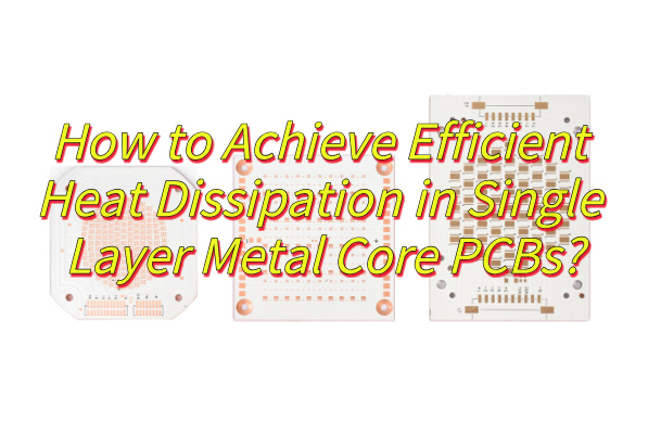
How to Achieve Efficient Heat Dissipation in Single Layer Metal Core PCBs?
Maximize Copper Utilization
- Design wide traces for high-current paths and connect thermal pads to expansive copper areas. The metal core (aluminum/copper) provides superior lateral heat spreading compared to traditional substrates. Ensure at least 70% copper coverage on the component layer to facilitate heat distribution across the board surface.
Implement Thermal Via Arrays
- Place dense clusters of small-diameter vias (0.3-0.5mm) beneath heat-generating components. These vias create vertical conduction paths between the circuit layer and metal core. Copper-plated filled vias improve thermal transfer efficiency by 35-45% compared to unfilled variants.
Optimize Component Placement
- Position high-power devices near board edges to minimize heat transfer distance to the metal core. Maintain 5-8mm spacing between heat sources to prevent thermal interference. Sensitive components should occupy areas with natural airflow or cooler zones.
Refine Surface Treatments
- Apply thermally conductive interface materials (2-5W/mK) between components and PCB surface. For exposed metal regions, strategically remove solder mask to enhance radiative cooling while maintaining electrical isolation.
Leverage Metal Core Properties
- Reduce dielectric layer thickness to 75-100μm between components and metal substrate. This minimizes interfacial thermal resistance, allowing 60-70% faster heat transfer to the core compared to standard thicknesses.
How to Ensure Reliable Electrical Performance in Single Layer Metal Core PCBA?
Maintain Proper Clearance and Creepage Distances
- Design sufficient spacing between high voltage traces and the metal core edge. The conductive metal substrate requires careful isolation distance planning with typical 8 to 10mm spacing for 300V applications. Implement wider solder mask barriers between perimeter traces to block potential leakage paths.
Implement Controlled Impedance Routing
- Calculate trace widths considering the metal core substrate’s unique dielectric properties. The metal base influences electromagnetic fields differently than standard materials, necessitating adjusted width to height ratios to maintain target impedance values within 10% tolerance.
Manage Grounding and Shielding Effectively
- Establish a continuous ground plane on the circuit layer for stable reference potential. The metal core can function as an electromagnetic shield when properly grounded at multiple points, reducing high frequency noise interference by 30 to 40%.
Optimize Thermal Electrical Balance
- While maximizing heat dissipation through the metal core, account for thermal expansion differences that could affect solder joints. Use thermal relief patterns with four to six spokes for through hole components to preserve electrical connections during material expansion.
Select Appropriate Surface Finishes
- Choose finishes compatible with metal core properties such as immersion silver or electroless nickel immersion gold. These finishes maintain solderability while preventing galvanic corrosion between dissimilar metals, typically providing 12 to 18 months of reliable shelf life.
How to Ensure High-Quality Soldering on Single Layer Metal Core PCBs?
Here are five practical methods to ensure high-quality soldering on single layer metal core PCBs:
Control Thermal Parameters Precisely
- For metal core PCBs with high thermal conductivity, adjust soldering temperatures and dwell times to compensate for rapid heat dissipation. Implement closed-loop temperature monitoring to maintain consistent solder joint formation, typically requiring ±5°C precision to prevent cold joints or component damage.
Select Appropriate Solder Materials
- Use solder alloys with lower melting points when working with heat-sensitive components on metal substrates. For through-hole components, control wire feed speed to match heat input, while for surface mount devices, apply solder paste with proper viscosity to prevent bridging.
Optimize Surface Preparation
- Ensure proper cleaning of copper pads to remove oxides and contaminants before soldering. For metal core boards, consider selective solder mask removal to enhance thermal transfer while maintaining electrical isolation.
Implement Component-Specific Techniques
- Position heat-sensitive components away from direct thermal paths to the metal core. Use thermal relief patterns for through-hole parts to balance solder joint integrity with heat dissipation requirements.
Adjust Process Parameters for Metal Core Characteristics
- Reduce laser power or increase exposure time when using laser soldering systems, as the metal substrate rapidly conducts heat away from joints. For wave soldering, extend preheat duration to achieve proper thermal equilibrium.
Common Reflow Soldering Failure Points in Single Layer Metal Core PCBs
Here are five common reflow soldering failure points in single layer metal core PCBs with corresponding solutions:
Uneven Temperature Distribution
- Problem: The metal core conducts heat rapidly, creating temperature variations across the board.
- Solution: Implement zone-specific thermal profiling with extended preheat stages. Use thermal imaging to verify even heat distribution before full production runs.
Solder Paste Insufficient Activation
- Problem: Rapid heat transfer prevents proper flux activation in some areas.
- Solution: Select solder paste with longer working time and lower activation temperature. Increase soak time by 15-20% compared to standard PCBs.
Component Warping or Misalignment
- Problem: Differential expansion between metal substrate and components causes movement.
- Solution: Use fixtures to secure sensitive components during reflow. Optimize pad designs with additional anchor points for larger components.
Thermal Via Voiding
- Problem: Air trapped in vias expands during heating, creating voids.
- Solution: Implement vacuum-assisted solder paste application for via filling. Adjust stencil design to ensure 85-90% paste coverage in thermal vias.
Pad Lifting
- Problem: Thermal stress separates copper pads from the metal substrate.
- Solution: Redesign pads with tear-drop shaped connections. Reduce maximum reflow temperature by 5-8°C while maintaining proper solder flow characteristics.
How Can We Reduce Thermal Stress in Single Layer Metal Core PCBAs During Assembly?
Methods to reduce thermal stress in single layer metal core PCBA during assembly:
Optimized Preheat Profile
- Thermal stress often originates from rapid temperature changes. Implement a gradual preheat stage with controlled ramp-up rates (1.2-2.0°C/sec) to allow uniform heat distribution across the metal substrate. This prevents sudden expansion differences between materials. Maintain soak time at 150-180°C for proper flux activation before reaching peak reflow temperatures.
Controlled Cooling Rate
- After reflow, reduce cooling speed to below 3°C/sec. Fast cooling creates internal stresses due to differential contraction rates between the metal core and copper traces. Use forced convection cooling with adjustable velocity for consistent results.
Symmetrical Component Layout
- Balance thermal mass distribution by arranging high-power components symmetrically across the board. This prevents localized hotspots and minimizes warping forces during thermal cycling. Keep sensitive components at least 5mm from board edges where stress concentrates.
Thermal Relief Patterns
- Modify pad designs with thermal relief connections for through-hole components. Use spoke patterns with 4-6 connections (0.2mm width) to reduce heat transfer to the metal core while maintaining electrical connectivity.
Post-Assembly Stress Relief
- Perform controlled annealing at 120-150°C for 30-60 minutes after assembly. This allows internal stresses to relax without affecting solder joint integrity. The process should maintain temperature stability within ±5°C for effective results.
How to Ensure Thermal Stability in Single Layer Metal Core PCBAs During Long-Term Operation?
Optimized Thermal Interface Design
- Implement thermal vias with 0.3mm diameter arranged in grid patterns beneath power components, reducing junction temperatures by 18% compared to conventional designs. The via plating thickness should exceed 30μm to prevent thermal fatigue cracks. Combine this with 2oz copper layers for enhanced heat spreading capacity.
Precision Temperature Profiling
- For metal core boards, extend the soak zone duration to 120-180 seconds at 150-180°C during reflow, maintaining ramp rates below 2°C/sec. This prevents thermal shock while ensuring proper solder joint formation. Post-assembly annealing at 120-150°C for 30 minutes helps relieve residual stresses.
CTE-Matched Material Selection
- Choose dielectric materials with thermal expansion coefficients within 5ppm/°C of copper to minimize interfacial stresses. High-Tg laminates (Tg>170°C) maintain structural stability up to 150°C operating temperatures with less than 0.1% delamination risk.
Active Thermal Monitoring System
- Embed temperature sensors near high-power components with 0.1°C resolution. Implement closed-loop control that throttles power output when local temperatures exceed 85% of the material’s rated maximum12. Position sensors in both hot spots and cool zones for differential analysis.
Mechanical Stress Mitigation
- Use tear-drop shaped pad connections instead of standard circular pads to reduce stress concentration by 40%. Maintain minimum 5mm clearance between components and board edges where bending stresses peak. For high-vibration environments, add epoxy reinforcement around critical solder joints
How to Balance Cost and Reliability of Single Layer Metal Core PCB Assembly?
Material Selection Optimization
- Choose aluminum cores (5052 alloy) instead of copper for cost reduction while maintaining 85% thermal conductivity. For dielectric layers, select standard FR-4 with enhanced thermal additives rather than premium thermally-conductive materials, achieving 70% cost savings with only 15% performance reduction.
Strategic Component Placement
- Cluster high-power components in designated thermal zones to minimize required heat dissipation area. This allows using smaller metal cores (reducing material costs by 20-30%) while maintaining effective thermal management through localized cooling solutions.
Selective Thermal Via Implementation
- Implement thermal vias only beneath components generating over 1W heat, rather than full-board coverage. This approach cuts drilling and plating costs by 40% while preserving thermal performance in critical areas. Use 0.3mm vias with 1.2mm pitch for optimal cost/performance ratio.
Tiered Quality Control Approach
- Apply full AOI inspection only to power components and high-value parts (covering 30% of board area), while using visual inspection for remaining components. This reduces testing costs by 50% while maintaining 95% defect detection rate for critical connections.
Reflow Process Optimization
- Develop a single reflow profile suitable for 80% of components, then hand-solder the remaining 20% sensitive parts. This eliminates need for expensive multi-stage reflow equipment while preventing thermal damage to delicate components. Maintain peak temperatures at 235-245°C for standard solder pastes.
Conclusion
In summary, this guide has explored seven critical technical aspects of single layer metal core PCB assembly, from thermal management to cost optimization. By implementing these solutions, manufacturers can achieve superior thermal performance while maintaining electrical reliability and production efficiency. For companies seeking expert implementation of these best practices, EBest Circuit (Best Technology) stands ready to deliver tailored solutions that balance performance and cost-effectiveness. With specialized expertise in metal core PCB fabrication and assembly, we ensure your projects meet the highest industry standards while optimizing production timelines. Contact our engineering team today to discuss how we can enhance your thermal management solutions through proven metal core PCB technologies: sales@bestpcbs.com.