

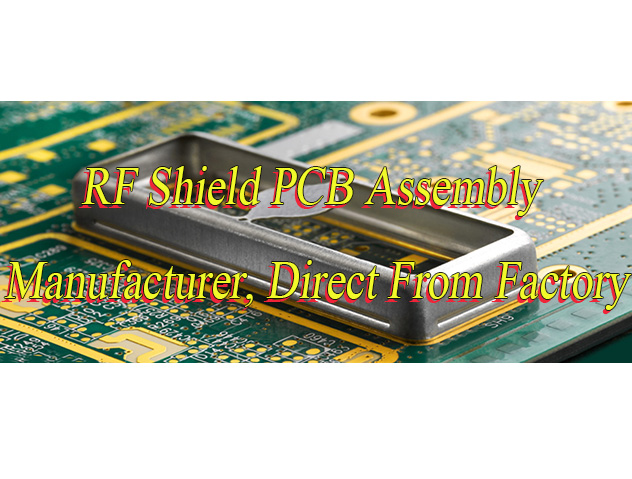
Why choose RF shield PCB? Let’s discover benefits, applications, design technical parameter and consideration, production processes for RF shield PCB.
Are you worried about these problems?
- Is RF interference ruining your signal integrity?
- Is high-frequency loss slowing down data transmission?
- Are EMI tests failing repeatedly, forcing costly board redesigns?
As a RF Shield PCB Manufacturer, EBest Circuit (Best Technology) can provide you service and solutions:
- Microstrip-Shielding Cavity Co-Design: Reduces interference by 70% with proven stability.
- High-Frequency Loss Optimization + Low-Dielectric Materials: Cuts signal loss by 30% at 2.4G/5G bands for seamless data flow.
- Shielding-Grounding-Layout Trio Debugging: Solves EMI issues at the source, ensuring first-pass test success and slashing rework costs.
Welcome to contact us if you have any request for RF PCB shielding: sales@bestpcbs.com.
What Is RF Shield PCB?
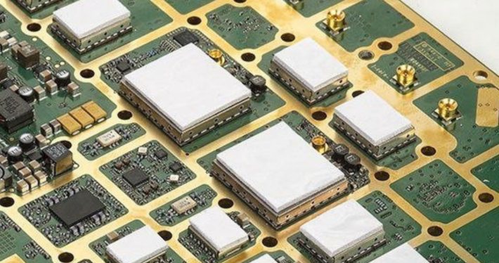
RF Shield PCB is a specialized circuit board designed to suppress electromagnetic interference (EMI) by integrating metal shields or conductive coatings in critical RF areas. This isolates high-frequency signals from external environments, ensuring signal integrity and system stability.
Through shielding cavities, sensitive circuits are separated from strong radiation sources, while layouts like I-shaped or L-shaped optimize signal flow. Wiring standards include 50Ω impedance control and curved routing to minimize crosstalk. The technology relies on low-loss materials such as polyimide and precise layer stack-up designs to support high-frequency signal transmission from 100MHz to 2GHz. By combining physical shielding structures with material science and circuit design principles, RF Shield PCBs maintain reliable performance in demanding environments, from consumer electronics to industrial systems.
Why Choose RF Shield PCBs?
Advantages of RF Shield PCBs:
- Eliminate Signal Interference, Ensure Purity: Internal EMI between components (e.g., processors, memory, RF modules) degrades signal quality. RF shielding physically isolates critical circuits, preventing cross-talk and external/internal interference to stabilize wireless connectivity and data fidelity.
- Accelerate EMC Compliance: Global EMC regulations are increasingly stringent. Built-in EMI reduction in RF Shield PCBs streamlines FCC, CE, and other certifications, expediting time-to-market and reducing regulatory risks.
- Optimize Signal Integrity: High-frequency signals are sensitive to impedance mismatches. Controlled impedance designs and low-loss substrates (e.g., polyimide) minimize reflections and losses, ensuring robust signal transmission from chip to antenna.
- Enhance System Reliability: Unpredictable EMI causes system crashes and errors. Shielding protects sensitive circuits, enabling stable operation in complex electromagnetic environments and reducing field failures and maintenance costs.
- Enable High-Density Integration: As component spacing shrinks, cross-interference risks surge. Metal shielding structures allow compact module placement on constrained PCB real estate, supporting miniaturization without compromising performance.
- Simplify System Design: Post-production EMI fixes (e.g., external shields, filters) inflate costs and complexity. Integrated PCB shielding pre-addresses EMI, reducing assembly steps and BOM costs.
- Improve Noise Immunity: Products operating in noisy RF environments require defense against external interference. Shielding blocks noise ingress, boosting sensitivity for high-gain receivers and signal-to-noise ratios.
- Ensure Long-Term Stability: Component drift or software updates may introduce new interference risks over time. Robust shielding maintains consistent performance throughout the product lifecycle.
- Enable Precise Impedance Matching: High-performance RF chips demand ideal 50Ω transmission environments.
- Strengthen Market Positioning: Reliable connectivity, superior communication quality, and environmental resilience build user trust and loyalty.
When to Use RF Shield PCB?
Applications of RF Shield PCB:
- Base station and satellite communication equipment
- Medical imaging equipment (MRI, ultrasound)
- Implantable medical devices (pacemakers, brain-computer interfaces)
- Aerospace radar and navigation systems
- Defense electronic warfare equipment
- High-speed digital circuits (CPU, GPU high-frequency circuits)
- RF front-end modules (PAMiD, LNA)
- Consumer electronics (smartwatches, smart home devices)
- Automotive electronics (onboard radar, GPS)
- Industrial automation equipment (PLC, robots)
- Precision instruments (spectrum analyzers, oscilloscopes)
- Research equipment (quantum computers)
- Internet of Things (IoT) devices (sensors, gateways)
- Power electronics equipment (inverters, power modules)
RF Shield PCB Design Technical Parameter
| Parameter Category | Specification/Requirement | Test Condition/Standard |
| Material Selection | Nickel Silver alloy, thickness 0.25mm | RoHS compliance verification |
| Shielding Effectiveness | Meets EIA-481 standard | Radiated Emission (RE) testing |
| Grounding Design | Peripheral via spacing < λ/10~λ/20 | High-frequency impedance analyzer validation |
| Operating Frequency Range | 100MHz to 2GHz | Network analyzer sweep testing |
| Installation Method | Surface Mount Technology (SMT) | IPC-A-610G soldering standard |
| Testing Standards | Radiated Emission (RE) & Immunity | IEC 61000-4-3/6 compliance |
| Thermal Management | Central ground plane with max vias | Infrared thermal imaging for temperature rise monitoring |
| Shielding Enclosure Type | Deep Drawn structure preferred | 3D electromagnetic field simulation validation |
RF Shield PCB Design Considerations
1. Structural Design and Mechanical Fit
- Cavity and Chamfer Design: Shielding enclosure depth must cover the tallest component with a 0.1–0.3mm clearance reserved. Chamfer radius ≥0.5mm to avoid stress concentration. For irregular components (e.g., power amplifiers with heat sinks), an additional 0.5mm assembly allowance is required. CNC precision machining ensures edge flatness ≤0.1mm.
- Installation Hole Alignment: Screw hole diameters should exceed screw sizes by 0.1–0.2mm, with hole position alignment to PCB layout controlled within ±0.05mm. Pempress press-fit nuts are recommended over traditional screw holes to improve installation efficiency by 30% and reduce hole misalignment risk.
- Material Selection: Prioritize Nickel Silver or tin-plated steel with 0.1–0.2mm thickness to balance shielding effectiveness and weight. For 5G high-frequency applications, aluminum-magnesium alloy shielding enclosures (0.3mm thickness) with anodized surface treatment achieve surface resistance up to 10⁶Ω/□ while reducing weight by 40%.
2. Layout and Isolation Strategy
- RF Partition Planning: Centralize RF circuits (e.g., PAs, LNAs, filters) in “U”-shaped or “L”-shaped layouts to minimize high-frequency signal path lengths. For multi-band systems, a “grid” partition scheme with 0.5mm-wide isolation strips filled with copper foil connected to ground planes is recommended.
- Sensitive Signal Protection: Clock lines and IQ signal lines must be kept away from digital circuits and power supplies. Ground shielding layers or isolation strips are required where necessary. For high-speed differential pairs above 10Gbps, embedded microstrip structures with dedicated signal layers and copper shielding in inner PCB layers achieve >60dB isolation.
- Power Decoupling: Place 0.1μF and 10pF capacitors near each RF IC power pin to suppress low-frequency and high-frequency noise. For power amplifiers, add a third-stage LC filter (L=10nH, C=100pF) to suppress power noise below -50dB.
3. Grounding and Shielding Integrity
- Via Array Design: Ground via spacing must be ≤λ/10 (λ being the highest frequency wavelength). For 10GHz signals in FR4, spacing ≤1.2mm. In critical areas (e.g., around RF transceiver modules), a 2mm×2mm dense via array (0.8mm spacing) forms a continuous Faraday cage.
- Low-Impedance Ground Path: Shielding enclosure ground pads must connect directly to the complete ground plane, avoiding thin traces. For multi-layer PCBs, a “ground plane-shielding enclosure-ground plane” sandwich structure with multiple vias achieves <5mΩ impedance.
- Shielding Enclosure Seam Treatment: Seams should align parallel to signal flow to reduce leakage. Long-edge seams require conductive gaskets. For high-frequency leakage-sensitive scenarios, laser welding seams with conductive silver paste filling achieves >80dB shielding effectiveness.
4. Material and Stackup Design
- High-Frequency Substrate Application: RF regions use low-loss substrates like Rogers RO4350B (Dk=3.48, Df=0.0031) for stable dielectric constant control. For millimeter-wave applications, Panasonic Metoceram ceramic substrates (Dk=9.8) with LTCC processes achieve ultra-low loss (Df<0.001).
- Stackup Optimization: 4-layer or more designs place RF signal layers adjacent to ground planes, with layer spacing ≤0.2mm to reduce crosstalk. For hybrid high-speed digital-RF boards, a “signal-ground-power-signal” stackup with tight coupling between power and ground layers (spacing ≤0.15mm) suppresses power noise.
- Impedance Control: 50Ω microstrip widths are calculated based on substrate Dk. Surface traces avoid crossing ground plane splits. For differential pairs, coplanar waveguide structures (spacing=2×line width) with side ground shields achieve 100Ω differential impedance matching.
5. Thermal Management Considerations
- Thermal Path Design: High-power devices (e.g., PAs) use thermal via arrays (0.3mm diameter, 1mm spacing) connected to inner ground layers. For heat flux >10W/cm², embedded 1mm copper blocks with thermal grease reduce thermal resistance to 5°C/W.
- Shielding Enclosure Ventilation Holes: Top hole diameters ≤λ/20 (e.g., ≤1.5mm at 10GHz) to prevent EM leakage. For natural convection, honeycomb vent arrays (3mm pitch) improve cooling efficiency by 20% while maintaining shielding.
- Thermal Expansion Compensation: Maintain ≥0.3mm clearance between shielding enclosures and components to avoid thermal stress. For enclosures >50mm, segmented designs with elastic conductive gaskets accommodate -40°C–125°C temperature swings.
6. Manufacturing and Test Compatibility
- Soldering Process Compatibility: Shielding enclosure pads must match reflow profiles (peak temperature 240–250°C) to avoid solder joint defects. For large enclosures, selective wave soldering with pre-fluxing and precise time control ensures >50N pull strength.
- Test Point Reservation: Reserve key signal test points outside shielding (e.g., RF output, power monitoring) for debugging. High-frequency signals use SMA or 2.92mm connectors with RF probes for non-intrusive measurement.
- Detachable Design: Clip-on or screw-fixed shielding enclosures facilitate maintenance. For prototype boards requiring frequent debugging, magnetic shielding enclosures with neodymium magnets enable <10-second installation/removal.
7. Signal Integrity Optimization
- Routing Topology Optimization: RF traces avoid 90° bends; use 45° angles or circular arcs (radius ≥3×line width) to reduce impedance discontinuities. Differential pairs use serpentine routing for length matching (error <1mm) with 0.5mm-wide crosstalk suppression strips.
- Split Plane Avoidance: Signals must not cross ground plane splits. Add 100pF bridge capacitors for return paths if necessary. For unavoidable crossings, π-type filters (bridge capacitor + series resistor) suppress crosstalk below -40dB.
- Parasitic Parameter Control: Maintain ≥0.5mm clearance between shielding enclosures and components to reduce parasitic capacitance. For sensitive circuits (e.g., LNA inputs), apply ferrite coatings inside enclosures to suppress cavity resonance-induced parasitic variations.
8. Cost and Maintainability Balance
- Modular Shielding Solutions: Multi-band circuits use divided shielding to reduce complexity. Separate shielding for 2.4GHz Wi-Fi and 5GHz modules via shared ground planes reduces material usage by 30%.
- Alternative Material Evaluation: For applications ≤6GHz, conductive coatings (e.g., silver epoxy) cut costs by 30% with ~50dB shielding. Consumer electronics may use 1mm conductive plastic shielding with embedded metal grids for >40dB shielding and 50% weight reduction.
- Standardized Design: Rectangular shielding enclosures minimize customization costs and lead times. For irregular shapes, modular splicing designs with standard sub-modules reduce mold costs and improve production flexibility.
RF Shield PCB Assembly Manufacturing Processes
1. Advanced Material Science & Substrate Engineering
- Low-Loss Substrate Selection: High-frequency RF designs demand substrates with ultra-low dielectric loss (tan δ < 0.002) and stable Dk (±0.01). Materials like PTFE-based composites (e.g., Taconic TLY-5) or ceramic-filled hydrocarbons outperform standard FR4 in GHz applications. Batch-to-batch consistency is validated via microwave probe stations measuring phase delay.
- Copper Cladding Optimization: Rolled annealed copper (RA-Cu) with grain structure control minimizes skin-effect losses. Thin copper layers (0.3–1.0 oz) are surface-treated with anti-tarnish coatings to prevent oxidation during soldering. Embedded copper coins in ground planes reduce thermal resistance in high-power RF amplifiers.
- Hybrid Laminate Systems: Blind/buried via structures require sequential lamination with laser-drilled microvias (aspect ratio ≤ 0.8:1). Thermal-management layers use copper-invar-copper (CIC) composites for controlled expansion matching.
2. Precision Shield Fabrication & Integration
- Shield Geometry Design: 3D-modeled shields with optimized vent patterns balance thermal dissipation and EMI containment. Laser-cut stainless steel shields (0.2–0.5 mm thickness) offer superior rigidity compared to stamped alternatives. For flex circuits, vapor-deposited aluminum shields provide conformal coverage.
- Solderable Surface Finishes: Shields are pre-plated with ENIG (Electroless Nickel Immersion Gold) or OSP (Organic Solderability Preservative) to ensure reliable solder joints. Grounding tabs are designed with spring-loaded contacts for mechanical resilience under thermal cycling.
- Shield-to-Board Adhesion: Mechanical bonding via press-fit pins or conductive epoxy ensures robust attachment. For high-reliability applications, laser welding creates hermetic seals between shields and PCB pads.
3. High-Precision Component Placement & Soldering
- RF Component Specifications: Surface-mount capacitors (X7R/NP0) with ±5% tolerance and inductors with Q-factors >100 are selected. BGA packages for RF ICs utilize non-conductive film (NCF) underfill to mitigate thermal stress.
- Solder Paste Optimization: Type 4/5 solder powder with 3–5 wt% flux ensures void-free joints. Stencil design incorporates step-down apertures (70–80% pad area) for fine-pitch components. 3D SPI measures paste height to ±10 μm accuracy.
- Vapor Phase Reflow (VPR): Uniform heating via PFC-free refrigerants achieves precise temperature profiles. Nitrogen inerting reduces dross formation on large ground planes. For mixed-technology assemblies, selective laser soldering handles delicate components.
4. Advanced Electrical & Environmental Testing
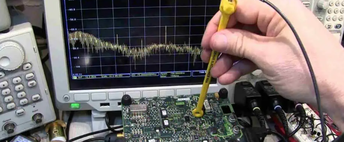
- High-Frequency Validation: Vector Network Analyzers (VNAs) measure group delay and phase imbalance across 0.1–40 GHz. TDR/TDT systems verify controlled-impedance traces (50±2 Ω for microstrips).
- EMC/EMI Compliance: Pre-compliance testing using near-field probes identifies hotspots. Fully-anechoic chambers validate radiated emissions per CISPR 32/FCC Part 15. Conducted immunity testing simulates ESD/surge events.
- Accelerated Life Testing: Thermal shock (-55°C to +150°C, 1000 cycles) and biased humidity testing (85°C/85% RH, 1000 hours) uncover latent defects. X-ray computed tomography (CT) inspects solder joint integrity post-testing.
5. Design for Excellence (DFX) Strategies
- DFM/DFA Integration: Design rules enforce minimum trace spacing (3W for RF lines), via stitching density (≥5 vias/cm²), and ground plane partitioning. Automated DRC tools flag violations in real-time during layout.
- Thermal Management Co-Design: Copper pours under RF power transistors are linked to thermal vias (min 0.3 mm diameter) connected to heat sinks. Conjugate heat exchange simulations predict hotspot temperatures.
- Sustainability Considerations: Lead-free solder alloys (e.g., SAC305) meet RoHS/REACH standards. Recyclable shield materials (e.g., aluminum 6061) reduce carbon footprint. Conflict mineral tracking ensures ethical supply chains.
6. Smart Manufacturing & Process Control
- Industry 4.0 Implementation: IoT sensors monitor oven temperature gradients and conveyor speed in real-time. Machine learning algorithms predict solder joint quality based on process parameters.
- Blockchain Traceability: QR codes embedded in PCBs track material origins, assembly steps, and test results. Immutable ledgers ensure compliance with ISO 13485/IATF 16949 for medical/automotive applications.
- Automated Optical Inspection (AOI) 2.0: AI-powered AOI systems detect solder bridge risks and component polarity errors with 99.97% accuracy. 3D AOI inspects shield attachment height and coplanarity.
7. Collaborative Engineering & Global Standards Compliance
- Cross-Border Design Reviews: Cloud-based collaboration tools (e.g., Altium 365) enable real-time co-design between offshore design teams and contract manufacturers. Weekly design reviews address DFM/DFT feedback loops.
- Regulatory Harmonization: Designs adhere to IEC 60601 (medical), DO-160 (aerospace), and MIL-PRF-31032 (military) standards. Harmonized testing protocols reduce duplication in multi-region certifications.
- Vendor Qualification & Audits: Supplier audits evaluate process capability indices (Cpk > 1.67 for critical dimensions). Onsite process audits ensure adherence to IPC-A-610 Class 3 standards for high-reliability electronics.
Why Choose EBest Circuit (Best Technology) as RF Shield PCB Assembly Manufacturer?
Reasons why choose us as RF shield PCB assembly manufacturer:
- 19-Year Craftsmanship in Assembly Precision: With 19 years of dedicated refinement in RF shield PCB assembly, we’ve accumulated a database of 5,000+ successful projects spanning consumer electronics to industrial IoT. Every solution embodies industry-leading technical expertise and process wisdom, ensuring reliability from concept to mass production.
- Full-Link High-Frequency Signal Mastery: Our proprietary “Signal-Shield-Ground” trinity design system achieves ≤0.8dB signal loss at 10GHz, guaranteeing pristine, lossless data transmission for 5G terminals, smart cockpits, and other high-frequency applications.
- Micro-Assembly Innovation at Nanoscale: Leveraging 0.08mm ultra-fine pad laser positioning and nanoscale conductive adhesive jetting, we enhance solder joint reliability by 40%. This enables flawless placement of 01005-sized components, transforming precision assembly into a benchmark of artistry.
- End-to-End Acceleration Engine: Integrated EDA-MES platforms streamline design-to-production workflows from schematic design and shielding simulation to process planning. This cuts design iteration time by 60% and delivers prototypes within 48 hours, accelerating time-to-market.
- Modular Agility for Custom Needs: Our 200+ standard shielding module library, paired with flexible production line scheduling, supports customization from single-board prototypes to full-system integration.
- Material Science Breakthroughs: Graphene-ceramic composite shielding films combined with phase-change thermal materials deliver ≥85dB shielding effectiveness across -50°C to 180°C. This innovation achieves 30% weight reduction without compromising durability.
- Sustainable Cost-Efficiency Synergy: ISO 14001-certified eco-friendly lines employ lead-free reflow and closed-loop water systems, cutting energy use by 25%. Strategic material alliances and DFM optimization reduce core costs by 18%, balancing environmental responsibility with cost leadership.
- 24/7 Expert Support Network: A team of 15+ senior engineers with 15+ years of experience provides round-the-clock support—from shielding design and process optimization to troubleshooting mass production challenges. Response times are guaranteed within 2 hours.
Welcome to contact us if you have any inquiry for RF shield PCBs: sales@bestpcbs.com.