

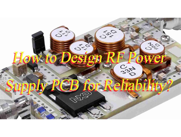
How to design RF power supply PCB for reliability? This blog is mainly about material selection, impedance control, thermal management, and EMI suppression for RF PSU PCB design.
Are you troubled these problems with RF power supply PCB?
- Does your RF power supply PCB suffer from unstable output power and efficiency degradation due to high-frequency signal crosstalk?
- Are thermal management challenges in high-speed RF modules causing overheating risks and performance decay?
- Do long lead times and uncontrolled costs during small-batch trial production delay your market entry opportunities?
As a RF power supply PCB manufacturer, EBest Circuit (Best Technology) can provide you service and solutions:
- High-Frequency Signal Optimization: Full-chain simulation from stack-up design to impedance matching ensures signal integrity and stable power output.
- Intelligent Thermal Management: Advanced thermal conductive materials and optimized layout design reduce heat buildup, extending module lifespan by 30%.
- Agile Supply Chain Support: Rapid prototyping with 7-day sample delivery and flexible production scaling achieves 15-day mass production readiness, accelerating time-to-market while controlling costs.
Welcome to contact us if you have any request for RF power supply PCB: sales@bestpcbs.com.
RF Power Supply PCB Material Selection for Reliability
Below Is RF Power Supply PCB Material Selection Guide:
- Prioritize low-loss dielectric materials: For high-frequency environments, select substrates with stable dielectric constant (Dk) and low loss tangent (Df), such as PTFE or hydrocarbon resin-based materials. This minimizes signal attenuation and thermal losses, ensuring efficient power conversion.
- Ensure thermal-mechanical compatibility: Match the coefficient of thermal expansion (CTE) of the material with copper foil and chip packaging materials. This prevents delamination, cracks, or long-term reliability degradation caused by thermal stress during high-temperature soldering or power cycling.
- Enhance environmental resilience: For high-humidity, high-temperature, or corrosive environments, use moisture-resistant and chemically inert coating materials (e.g., modified rosin resins) or surface treatments. This prevents dielectric absorption, copper migration, or insulation failure.
- Balance cost and performance: Select materials based on power levels and application scenarios. High-frequency, high-power designs may require premium low-loss substrates, while mid/low-frequency applications can leverage cost-effective FR-4 variants. Validate reliability through multi-physics simulations (thermal-electrical-mechanical coupling).
- Verify manufacturing process compatibility: Confirm materials align with existing PCB fabrication processes (e.g., lamination temperatures, drilling parameters, surface finishes). Avoid issues like inner-layer voids, pad lifting, or impedance variations that compromise yield and long-term reliability.
Impedance Control in RF Power Supply PCB Design
- Core Goal of Impedance Matching: Ensure signal path impedance aligns with source and load impedance to minimize signal reflection and power loss. In high-frequency scenarios, minor impedance deviations can cause signal distortion or reduced power transmission efficiency, requiring strict control within design tolerances.
- Critical Parameter Control: Maintain characteristic impedance at 50 ohms or 75 ohms (per system standards) with a typical error margin of ±10%. Focus on geometric dimensions of transmission lines (e.g., microstrip lines, striplines, coplanar waveguides), including trace width, spacing, dielectric thickness, and dielectric constant.
- Material Selection and Stack-Up Design: Prioritize low-loss substrates (e.g., Rogers series or high-frequency FR-4 variants) for stable dielectric constants. Balance signal, power, and ground layers in stack-up design to avoid inter-layer crosstalk. Multi-layer boards require clear inter-layer impedance coupling relationships and optimized inter-layer dielectric thickness.
- Layout and Routing Guidelines: Keep high-frequency signal traces short, straight, and minimize bends/vias. Isolate sensitive lines (e.g., power amplifier outputs) from digital signals to prevent cross-interference. Power paths should account for current capacity and voltage drop, using wide copper traces or parallel routing to reduce impedance.
- Grounding and Shielding Strategies: A continuous ground plane forms the foundation of impedance control; avoid splitting ground planes to prevent impedance discontinuities. Use localized shielding cans or ground via arrays in critical circuit areas to reduce electromagnetic radiation and external interference.
- Power Integrity Management: Control impedance fluctuations in the power distribution network using decoupling capacitor networks to suppress high-frequency noise. Place capacitors near power-consuming components to create low-impedance return paths and stabilize supply voltage.
- Thermal Management and Material Durability: Account for impedance variations with temperature in high-power RF circuits by selecting high-temperature-resistant substrates and surface finishes. Coordinate thermal design with impedance control to prevent dielectric deformation or impedance drift due to thermal stress.
RF Power Supply PCB Layout Optimization for Signal Integrity
1. Physical Partitioning and Electrical Isolation
Zone Division
- Strictly separate RF, digital, and power zones using “I-shaped” or “L-shaped” layouts to minimize signal path crossings.
- Avoid U-shaped signal paths to prevent self-interference.
Component Placement
- Isolate high-power amplifiers (PA) and low-noise amplifiers (LNA) by ≥1.5cm, placing them on opposite PCB sides to reduce thermal coupling.
- Dedicate shielded cavities for sensitive analog circuits (e.g., VCOs) with non-square aspect ratios to suppress resonance.
2. Impedance Matching and Transmission Line Design
Transmission Line Parameters
- Maintain 50Ω±5% characteristic impedance using microstrip, stripline, or coplanar waveguide based on stackup structure.
- Use 45° curved routing to reduce reflections; trace width ≥15mil (high-frequency scenarios), spacing ≥2W (W=1/10 signal wavelength).
Differential Pair Design
- Symmetrically route differential pairs with adjacent ground traces and via stitching; avoid parallel routing to prevent crosstalk.
- Limit via count in critical paths (e.g., antenna feedlines) to ≤3 per 10cm; backdrilled stub length ≤50μm.
3. Ground System Optimization
Ground Plane Integrity
- Employ continuous multi-layer ground planes (e.g., layer 2 as GND) without islanding or cuts.
- For frequencies >1GHz, implement multi-point grounding with signal return paths tightly adjacent to signal traces.
Via Placement
- Place ground vias every 1-2mm alongside key RF paths to form “fences”; match via placement for differential signals.
- Shield cans must connect to the ground plane at ≥3 points; aperture size ≤λ/10 to prevent high-frequency leakage.
4. Decoupling Capacitor Hierarchy
Tiered Decoupling System
- Chip-Level: 0402 1nF MLCC placed ≤1mm from BGA pins for high-frequency noise suppression.
- Module-Level: 0603 10nF+100nF combination for 100MHz-1GHz band; ensures low-impedance path.
- System-Level: 3216 4.7μF tantalum capacitor to mitigate low-frequency power ripple.
Grounding Consistency
- Ensure capacitor ground terminals share a common ground via direct connection to the ground plane; avoid series vias that cause ground potential inconsistencies.
5. EMC and Shielding Design
High-Power Region Isolation
- Reserve intact ground planes under high-power regions without vias to maintain signal integrity.
- Achieve ≥30dB isolation between RF output and input; add shielding if necessary.
Sensitive Signal Protection
- Shield sensitive signals (e.g., clock lines) using stripline routing with ≥10mil width, flanked by ground traces and vias.
- For digital/analog crossings, use layered routing with intermediate ground planes to prevent capacitive coupling.
6. Thermal Management
Heat Distribution
- Distribute heat evenly across the PCB to avoid local hotspots; use ≥2oz copper thickness under high-power devices.
- Connect high-power components to heatsinks using thermal adhesive/pads; use metallized mounting holes (≥3mm diameter) under PAs for enhanced heat dissipation.
Thermal Validation
- Validate thermal distribution via tools like Ansys to ensure temperature rise ≤40°C; consider thermal expansion coefficient matching.
7. Verification and Simulation Tools
Impedance Validation
- Verify impedance using SI9000 and TDR with ±5% tolerance; confirm resonance points via VNA frequency response testing (0.1-10GHz).
Reliability Testing
- Conduct thermal cycling tests (-55°C to 125°C) to validate long-term reliability; use Ansys HFSS/CST for electromagnetic field analysis to optimize shield can dimensions and via placement, ensuring first-pass EMC compliance.
Heat Dissipation Strategies for 100W RF Power Supply PCBs Design
1. High-Thermal-Conductivity Substrate Selection
- Metal Substrate Application: Replace traditional FR4 with aluminum substrate (thermal conductivity 2–5 W/m·K) or copper substrate (385 W/m·K) for high-heat devices like RF power amplifiers (RF PA) and MOSFETs. For example, aluminum substrates can reduce 100W MOSFET temperature from 95°C to 65°C, significantly enhancing reliability.
- Ceramic Substrate Solution: Aluminum nitride (AlN) or silicon carbide (SiC) ceramic substrates offer thermal conductivity of 170–200 W/m·K, suitable for high-frequency high-power scenarios such as 5G RF modules, preventing interlayer cracking due to mismatched thermal expansion coefficients.
- Thick Copper Foil Process: Use 4oz (140μm) or 6oz (210μm) copper foil with large-area power/ground copper foil design, achieving heat dissipation capacity exceeding 0.8W/cm² to meet 100W power requirements.
2. Thermal Flow Path Optimization Layout
- Device Zoning Strategy: Place high-heat devices (e.g., RF PA, DC-DC modules) at PCB edges or upper layers to shorten heat conduction paths. Position sensitive components (e.g., small-signal transistors, crystals) in cool air inlets, avoiding direct placement above heat sources.
- Thermal Via Array Design: Deploy dense 0.3mm-diameter thermal vias (spacing ≤0.6mm) beneath power devices to create low-thermal-resistance channels to bottom-layer heat sinks. For instance, 100W RF PA with 100 vias/cm² can lower temperature by 15°C.
- Airflow Management: Design airflow paths to avoid component obstruction, combining horizontal/vertical heat sinks with forced air cooling (fans) or natural convection to optimize airflow and ensure efficient hot air exhaust.
3. Active and Passive Heat Dissipation Synergy
- Heat Sink Selection: Aluminum fin heat sinks (fin height 10–20mm) suit 10–100W scenarios; above 100W, recommend water-cooled heat sinks or heat pipe systems (e.g., rocket-grade heat pipes) using phase-change principles for efficient heat transfer.
- Interface Material Application: Use thermal grease (3–5 W/m·K) or thermal silicone pads (2–4 W/m·K) to fill gaps between devices and heat sinks, reducing thermal resistance below 0.1°C/W and preventing thermal failure from air gaps.
- Liquid Cooling Integration: Embed microchannel liquid cooling structures in PCBs or adopt integrated coolant nozzles directly contacting high-heat device bases, enabling efficient heat dissipation via fluid circulation for enclosed chassis or high-density installations.
4. Thermal Simulation and Testing Verification
- Simulation Tool Application: Utilize software like ANSYS Icepak or FloTHERM for thermal simulation, identifying hotspots and optimizing copper foil layout, via density, and heat sink shapes. For example, adjusting via diameter and spacing via simulation can reduce thermal resistance by over 30%.
- Experimental Testing Methods: Monitor PCB surface temperature distribution with thermal imagers and collect real-time data via temperature sensors to validate heat dissipation design. Critical points (e.g., power device solder joints) require thermal cycling tests to ensure long-term reliability.
- Material Thermal Characteristic Verification: Test thermal expansion coefficients and conductivity of substrates (e.g., Rogers 4350B, aluminum substrates) to ensure compatibility with device parameters, preventing interlayer separation or solder joint failure due to thermal stress.
5. Process and Structural Innovation
- Mesh Copper Foil Design: Design large-area copper foil as mesh (minimum grid 0.025-inch) without compromising electrical performance, reducing soldering thermal stress and preventing copper foil blistering or board warping.
- Thermal Isolation Rings and Heat Dissipation Strips: For large pads or high-current traces, use thermal isolation rings to minimize soldering heat conduction impact on adjacent areas. Heat dissipation strip width should match pad diameter (typically 60% of pad diameter) to ensure concentrated heat export.
- Modular Heat Dissipation Solutions: Adopt standardized heat dissipation modules (e.g., fin heat sinks, heat pipe assemblies) with plug-and-play designs for easy maintenance and upgrades, while reducing overall system thermal resistance.
Best Practice for Grounding the Shield Can on an RF PSU PCB
1. Core Principles of Grounding Design
- Priority of Continuous Ground Plane: Multi-layer PCBs must feature a continuous full-layer ground plane (e.g., Layer 2 in a 4-layer board as the RF reference ground layer). Avoid fragmented or segmented ground islands to ensure low-impedance signal return paths (<0.1Ω@GHz band). Directly place ground planes beneath high-frequency signals to form microstrip/stripline structures, minimizing impedance discontinuities.
- Shortest Return Path: Critical RF signals (e.g., antenna feedlines, PA outputs) require “via fence” technology—dense grounding vias spaced every 1-2mm (≤λ/10) along signal paths, forming a Faraday shielding cage to suppress dipole antenna effects.
- Grounding Strategy Selection: High-frequency circuits (>100MHz) mandate multi-point grounding via dense vias (4-6 per cm²) connecting ground planes. Low-frequency circuits (<100MHz) may use single-point grounding to avoid ground loop noise.
2. Physical Grounding Specifications for Shield Cans
- Material & Contact Design: Shield cans prioritize tin-plated steel, copper, or aluminum with soldered or spring-loaded clip fastening. Solder pads must be ≥0.5mm wide, spaced ≤2mm, using high-conductivity solder (e.g., SnAgCu) or conductive adhesive for low-impedance contact. Removable shields require 360° contact via spring clips or conductive foam to prevent floating ground-induced shielding failure.
- Opening & Ventilation Control: Aperture size strictly limited to ≤λ/10 (e.g., 1.25cm for 2.4GHz signals). Ventilation holes must use honeycomb structures or metal mesh to prevent RF leakage.
- Edge Grounding Enhancement: PCB edges adopt metallized edge wrapping (copper width ≥2mm) or ground rings combined with spring-clip grounding to ensure low-impedance connections between shields and PCB edges, reducing parasitic resonance risks.
3. PCB Stackup & Structural Optimization
- Recommended Layer Stackup: Standard 4-layer configuration: Top layer (RF signal layer), Layer 2 (ground plane), Layer 3 (power layer), Bottom layer (signal layer). 2-layer boards must designate the bottom layer as a full ground plane, reserving the top layer for critical RF traces.
- Via & Grounding Network: Double-row via arrays spaced ≤1mm surround critical RF regions (e.g., LNA/PA modules) to form low-impedance return paths. Blind/buried vias suit high-density HDI boards, reducing via parasitic inductance.
- Mixed-Signal Isolation: Analog ground (AGND) and digital ground (DGND) are physically separated, connecting only at the power entry point via 0Ω resistors or ferrite beads to block high-speed switching noise coupling.
4. Optimization Measures & Validation Methods
- Case Study Evidence: 5G mmWave modules reduced EMI leakage by 20dB and crosstalk by 30% by shrinking ground pad spacing to 1.5mm, adding dual via rows (1mm spacing), and implementing spring-clip edge grounding. Wi-Fi modules restored receiver sensitivity and reduced error rates to <10⁻⁶ via local grid copper flood (≤λ/2 spacing) and via density up to 5/cm².
- Simulation & Measurement Synergy: Design phase uses Ansys HFSS/CST Microwave Studio for ground impedance and S-parameter simulation (target S₁₁<-10dB, S₂₁<-30dB). Measurement phase employs near-field probes and spectrum analyzers to validate shielding effectiveness per ETSI/FCC standards.
- Regulatory Compliance: Adheres to Radio Equipment Directive 2014/53/EU. Cable shields require 360° bonding to connector shells, avoiding “pig-tail” wiring to minimize inductance-induced high-frequency noise.
5. Special Scenarios & Key Considerations
- High-Speed SerDes Interfaces: Adopt coplanar waveguide (CPW) structures to ensure tight signal-ground coupling and reduce radiation loss.
- mmWave Band Challenges: >30GHz bands require exploration of 3D metallization packaging or nano-conductive materials, as conventional vias may fail. AI-driven simulation optimizes shielding structures.
- ESD Protection: Chassis ground connects to system ground via low-impedance paths, paired with TVS diodes to suppress transient disturbances, ensuring human safety and system stability.
RF Power Board Harmonic and EMI Suppression Solutions
1. Harmonic Suppression Core Strategies
- Use LC filter banks (e.g., π-type/T-type structures) to precisely suppress specific frequency harmonics. Recommend inductors with high saturation current and low core loss using ferrite material, and capacitors with X7R/X8R ceramic for balanced temperature stability and cost.
- For switching power modules, connect common-mode chokes + Y-capacitors in parallel at input/output terminals to suppress common-mode noise in 150kHz-30MHz range. Add series differential-mode inductors to filter differential-mode interference, ensuring compliance with CISPR 22 Class B standards.
2. EMI Source Control and PCB Layout Optimization
- High-frequency signal paths follow “short, direct, wide” principles: critical RF traces (e.g., PA output) should be ≤ λ/10 in length to avoid antenna effects; use ≥20mil copper thickness to reduce current density and parasitic inductance.
- Ground plane partitioning requires caution: analog/digital grounds connect via beads or 0Ω resistors at a single point to avoid ground bounce noise. High-speed signal layers should be adjacent to a solid ground plane (spacing ≤5mil) for low-impedance return paths.
- Sensitive components (e.g., LDOs, crystals) should be isolated from high-frequency areas using “thermal island” designs, with through-hole arrays for shielding to reduce crosstalk.
3. Shielding and Material Selection Practices
- Metal shielding cans use 1-2mm thick aluminum-magnesium alloy with nickel plating for oxidation resistance. Install conductive foam at openings for 360° grounding. For cavity resonance frequencies, apply absorber coatings (e.g., ferrite layers) to suppress standing waves.
- PCB substrates prioritize low-loss high-frequency materials like RO4350B/RO4003 (dielectric constant 3.48±0.05) with ENIG surface finish for solder reliability and reduced surface roughness impact on signal integrity.
4. Grounding System Design Standards
- Single-point grounding suits low-frequency scenarios (<1MHz); high-frequency modules adopt multi-point grounding connected to the bottom-layer ground plane to form low-impedance networks. For mixed-signal systems, recommend “star” grounding topology with the center point connected to chassis ground via low-impedance paths.
- Ground vias should be spaced 5-8mm apart to avoid ground loops. Critical interfaces (e.g., SMA, I/O) use ground springs for direct connection to metal enclosures, ensuring continuous low-impedance grounding paths.
5. Test Verification and Standards Alignment
- Pre-certification stages use near-field probes to scan PCB areas, locate over-limit frequencies (e.g., 100MHz, 300MHz), and optimize layouts or add filter capacitors. Formal testing requires 3m anechoic chamber radiation scans to meet FCC Part 15, EN 55032, and other international standards.
- Recommend real-time debugging with spectrum analyzers + near-field probes, complemented by EMI receivers for full-band scans. For harmonic issues, use oscilloscopes to observe power waveform distortions and supplement with harmonic compensation circuits (e.g., PFC circuits) to optimize power factors.
RF Power Supply PCB Design Verification Methodologies
1. Signal Integrity Verification
- Use Time-Domain Reflectometry (TDR) and Eye Diagram Analysis to verify high-speed signal integrity, ensuring no impedance discontinuity or reflection in RF signal transmission paths.
- Perform differential pair line width/spacing tolerance analysis, simulate signal loss under different process variations using tools like ADS/HFSS, and ensure design margin ≥20%.
- Conduct crosstalk simulation for critical signals (e.g., control lines, clock lines), with adjacent signal spacing adhering to the 3W rule (≥3× line width).
2. Power Integrity Verification
- Conduct DC Drop analysis on power planes to ensure voltage drop ≤2%, preventing localized voltage deficiency-induced device performance degradation.
- Analyze power noise coupling using power integrity tools (e.g., Sigrity), and design decoupling capacitor networks for high-frequency noise, with capacitance values matched to target impedance via Z-parameters.
- Implement dynamic voltage fluctuation testing, measure power ripple under actual operating conditions with an oscilloscope, and ensure ≤1% peak-to-peak value.
3. Thermal Management Verification
- Perform thermal distribution analysis using thermal simulation tools (e.g., FloTHERM), with junction temperatures of critical power devices (e.g., MOSFETs, LDOs) below 85°C safety threshold and 15% thermal design margin reserved.
- Design thermal paths including thermal pads/copper blocks, via arrays, and thermal pads, ensuring thermal resistance ≤10°C/W.
- Execute temperature cycling tests (-40°C to 125°C) to validate solder joint reliability and material CTE (Coefficient of Thermal Expansion) matching.
4. EMC/EMI Compliance Verification
- Conduct radiated emission pre-scans using near-field probes and spectrum analyzers, focusing on switching power noise, RF harmonics, and ground loop issues.
- Design low-impedance grounding networks with star-point grounding topology to avoid ground bounce noise, with ground plane coverage ≥80% of PCB area.
- Perform conducted emission testing (e.g., EN55022 standard), suppress high-frequency noise via filter capacitor/inductor combinations, and ensure conducted interference ≤40dBμV (30MHz–1GHz).
5. Manufacturability & Reliability Verification
- Execute Design Rule Checks (DRC) to ensure line width/spacing and via dimensions comply with fabricator capabilities (e.g., minimum 4mil line width, 8mil via diameter).
- Validate pad design compatibility (e.g., HASL/ENIG surface finishes) and BGA device pad symmetry.
- Conduct reliability acceleration tests (e.g., HAST, TC) to verify solder joint mechanical strength and material moisture/thermal resistance, ensuring MTBF ≥100,000 hours.
6. RF Performance Special Verification
- Measure RF power amplifier input/output impedance using network analyzers, tune matching networks via Smith charts, and ensure S11 ≤ -15dB (return loss).
- Implement power efficiency testing, measure PAE (Power-Added Efficiency) using power meters and DC supplies, with target ≥60% at operating frequency.
- Validate RF shielding effectiveness by measuring electromagnetic leakage in critical areas with near-field probes, ensuring shielding enclosure ground resistance ≤10mΩ and gap leakage ≤-50dB.
7. Collaborative Design & Verification Process
- Adopt EDA toolchains (e.g., Altium/Cadence) for schematic-PCB-simulation collaborative verification, ensuring real-time synchronization of design changes.
- Implement design review mechanisms with independent teams cross-verifying signal path integrity, PDN (Power Distribution Network) noise, and thermal design rationality.
- Establish a verification issue tracking system to classify discovered issues (Critical/Major/Minor) and formulate remediation plans, ensuring closed-loop management.
Feel free to contact us if you have any other issues for RF power supply PCB design: sales@bestpcb.com.