

Why is choosing the right Ceramic RF PCB manufacturer more important than “just picking a material”?
If you only remember one thing: the manufacturer’s process window can matter as much as the substrate choice. A perfect material spec won’t save you if copper adhesion, line definition, or ceramic handling is inconsistent. In ceramic boards, yield and reliability are heavily influenced by metallization method, copper thickness control, micro-pattern capability, and how the factory manages thermal stress during fabrication and assembly.
That’s why many engineering teams start by shortlisting a manufacturer that can do proper DFM, tolerance control, and traceability—then pick the final ceramic + copper system that fits the factory’s proven process. Ceramic PCB capability is commonly delivered through processes like DPC, DBC, AMB, thick film, LTCC/HTCC, each suited to different applications and costs.
Why pick EBest first when you need a Ceramic RF PCB manufacturer?
- Free DFM and process adaptation suggestions before you commit.
- 20 years experience, serving 1800+ customers and 10,000+ engineers (engineering-friendly communication cadence).
- One-stop service: PCB, components, PCBA, testing, and box-building.
- No MOQ, personal service, prototype & small volume welcome.
- Quality system coverage: ISO9001 / ISO13485, IATF16949, AS9100D.
- MES & Traceability for process accountability.
- 1.5-week rapid PCBA delivery (project-dependent) with quick-turn discipline.
- Technical support before & after sales, prompt feedback within 12 hours.
What is Ceramic RF PCB? Why to use it?
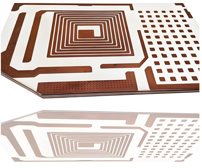
Ceramic RF PCB is a high-frequency circuit board built on ceramic substrates (commonly alumina Al2O3, aluminum nitride AlN, or beryllium oxide BeO) where copper is bonded or plated onto ceramic for RF signal stability and superior heat spreading. In plain terms: it’s chosen when you want RF to stay consistent at higher frequencies and power density without “temperature drift” turning your tuning into guesswork.
In RF builds, the board is not just a carrier. It becomes part of your circuit: it affects impedance, loss, phase, and even long-term drift. Ceramics stand out because they are electrically stable and mechanically rigid, while also handling harsh temperature environments better than typical organic laminates in many use cases. Ceramic substrates are widely recognized for RF and microwave suitability due to low dielectric loss and stable properties under operating conditions, and they’re also used in 5G, aerospace, automotive, and power modules in real production environments.
Where is Ceramic RF PCB most worth it in real RF/microwave products?
Ceramic RF PCBs are typically most “worth the cost” when your RF performance and thermal load rise together. In other words, you either run higher frequency where loss and drift matter more, or you run higher power where junction temperature threatens RF stability. Typical use cases include compact RF power amplifiers, antenna feed networks in tight space, RF front-end modules with hot components, and applications that need stable performance across wide temperature swings.
- RF and microwave modules where low dielectric loss and stability are valuable.
- High-power RF sections where heat must leave fast (reducing frequency drift and protecting components).
- Harsh environments: automotive, aerospace, industrial, and outdoor telecom enclosures.
- Miniaturized layouts where mechanical stiffness and dimensional stability help consistency.
Many ceramic PCB resources describe ceramics as suitable for RF/microwave due to low dielectric loss, stable permittivity, and robustness in demanding environments, alongside high-power and high-temperature use cases.
Alumina vs AlN vs BeO: how do beginners choose the right ceramic substrate?
Pick the substrate by answering four questions first:
(1) How much heat must move through the board?
(2) How sensitive is your RF response to temperature drift?
(3) Do you need fine lines and tight impedance control?
(4) Are there safety/compliance constraints?
Alumina is the common “balanced” option; AlN is usually chosen when thermal performance is critical; BeO can provide very high thermal conductivity but comes with safety handling constraints in many organizations.
| Parameter | Alumina (Al2O3) | Aluminum Nitride (AlN) | Beryllium Oxide (BeO) |
|---|---|---|---|
| Best for | Balanced RF + cost, common ceramic builds | High heat flux RF modules, power + RF combined | Extreme thermal needs (with strict safety policies) |
| Thermal conductivity (typical ranges) | Often cited around 20–30 W/m·K class in many industry references | Commonly cited ranges vary by grade; many sources cite ~140–200 W/m·K or broader ranges depending on grade | Often cited around 250–300 W/m·K class in industry references |
| RF stability | Good stability; widely used and well-understood | Very good, especially when temperature is a major variable | Good, but selection is often driven by thermal rather than RF-only reasons |
| Manufacturing maturity | Very mature supply chain | Mature, but cost and process control matter more | More restricted handling; fewer suppliers in many regions |
| Notes for beginners | Start here if your RF is sensitive but heat is moderate | Move here when your PA/LNA module runs hot or you need lower thermal resistance | Only choose if your organization allows BeO handling and you truly need it |
Quick selection rule
- If your RF module is “warm but not hot”: start with Alumina.
- If your hotspot is driving drift or reliability risk: shortlist AlN.
- If your design is extreme heat flux and policies allow: evaluate BeO carefully.
Which ceramic properties actually matter for RF engineers: Dk, Df, CTE, and thermal conductivity?
For RF, you care about how parameters interact: Dk affects impedance and electrical length; Df affects insertion loss; CTE mismatch drives solder and interface stress; thermal conductivity affects junction temperature and drift. A ceramic substrate is attractive because its dielectric behavior is stable, and it can survive harsh environments while helping heat move away efficiently.
How Dk affects impedance and phase
- Higher Dk generally allows smaller transmission line geometry for the same impedance, which can be good for miniaturization.
- But tighter geometry can increase sensitivity to etch tolerance and copper edge definition.
How Df affects loss at higher frequency
- Df (loss tangent) is a key driver of dielectric loss, which becomes more visible as frequency increases.
- For long RF traces, filters, and distributed elements, Df can be a performance limiter.
Why CTE matters more than many beginners expect
- CTE mismatch between ceramic, copper, and components can create stress during reflow or thermal cycling.
- This is one reason ceramic builds need a manufacturer who understands ceramic handling and metallization adhesion.
DPC vs DBC vs AMB: what’s the difference, and which metallization is best for Ceramic RF PCB?
Metallization is how copper “becomes one” with ceramic. The right choice depends on line/space needs, copper thickness, thermal cycling expectations, and cost. If you need fine features and smoother copper for precision RF patterns, DPC is often discussed as a strong option. If you need thick copper for heat spreading or power handling, DBC is common. AMB is often selected for robust bonding in demanding power modules and harsh cycling cases. Many ceramic PCB process references list DPC, DBC, AMB alongside thick film/thin film/LTCC/HTCC as core approaches.
| Metallization | How it’s formed (concept) | Strengths for RF | Common reasons to choose | Typical trade-offs |
|---|---|---|---|---|
| DPC (Direct Plated Copper) | Copper is plated onto prepared ceramic surface | Often enables finer lines and smoother copper for accurate RF patterning | Fine pitch RF, compact RF modules, controlled geometry | Process control critical; cost can be higher than basic thick film |
| DBC (Direct Bonded Copper) | Thick copper is bonded to ceramic under controlled conditions | Strong thermal spreading; stable copper thickness | Power + RF, heat spreaders, high current sections | Feature size can be less “fine” than DPC in some builds; heavier copper handling |
| AMB (Active Metal Brazing) | Active brazing alloy bonds copper to ceramic | Robust interface in demanding environments | High reliability modules, harsh thermal cycling | Cost and vendor availability may be higher; design must respect process limits |
Beginner mapping
- Need tight RF geometry and fine patterns? Start with DPC.
- Need thick copper and strong heat spreading? Look at DBC.
- Need very robust bonding for harsh cycling? Evaluate AMB.
How do you design controlled impedance on Ceramic RF PCB so it stays stable in production?
For beginners: controlled impedance is not “a calculator result,” it’s a manufacturing agreement. The most practical approach is to define your target impedance (50Ω single-ended, 100Ω differential), specify the stack and copper thickness, then let the manufacturer confirm geometry with their process capability and coupons. Ceramic RF builds benefit from stiffness and stability, but they also demand tight control of etching and copper definition because RF lines can be small and sensitive.
What to define for 50Ω / 100Ω before you route
- Substrate type and thickness (Al2O3 / AlN / etc.).
- Copper thickness (and whether copper is thick like DBC).
- Reference plane strategy (continuous ground return is non-negotiable in most RF layouts).
- Surface finish and solder mask strategy (some ceramic builds may differ from FR-4 norms).
Layout habits that reduce RF surprises
- Keep return paths short and continuous; avoid broken reference planes under RF traces.
- Use via fences where isolation matters, and keep via inductance in mind for transitions.
- For matching networks: place components tight, minimize interconnect length, and keep ground inductance low.
- Ask for impedance coupons and test reports as part of the build, not after a failure.
What are the most common production “failure modes” for ceramic RF boards, and how do you prevent them?
The fastest way to avoid headaches is to treat ceramic as its own manufacturing category. Common problems are not “RF math” problems—they’re thermo-mechanical and interface problems: cracking from thermal shock, copper-to-ceramic adhesion weakness, and assembly-induced stress. Ceramics are robust, but they can be unforgiving if the process ignores CTE mismatch and thermal profiles.
Typical risk points to watch
- Thermal shock during reflow or rework (profile discipline matters).
- Copper-ceramic interface stress (especially with thick copper systems).
- Board handling and depaneling method (laser depaneling is commonly discussed for clean ceramic edges).
- Component layout that concentrates stress near corners or cutouts.
Prevention checklist (beginner-friendly)
- Confirm assembly profile recommendations with your manufacturer early.
- Use appropriate pad and solder volume strategy to reduce stress.
- Specify edge and corner rules (avoid sharp internal corners; consider stress relief).
- Request traceability for materials and key process steps when reliability matters.
What DFM information should you confirm before ordering a Ceramic RF PCB?
Good DFM prevents most expensive RF mistakes. Before you order, align on manufacturable line/space, minimum feature sizes, hole and slot rules (if any), copper thickness tolerances, and how the metallization method impacts RF geometry. You also want a clear agreement on what will be tested and reported. Many ceramic PCB manufacturers highlight that different metallization processes fit different applications, so DFM is where you lock the right process for your design.
RF-focused DFM items
- Target impedance and coupon plan (what gets measured, where, and how reported).
- Allowed etch tolerance and copper edge definition for critical RF traces.
- Grounding strategy review (planes, stitching vias, via fences).
- Surface finish recommendation based on frequency and assembly.
Files and data to send for accurate quoting
- Gerbers or ODB++ plus drill files.
- Stack-up requirements and target impedance notes.
- BOM (if you want turnkey PCBA) and assembly drawings.
- Special requirements: cleanliness, inspection criteria, reliability tests.
How do you test and accept a Ceramic RF PCB so the quality is measurable, not “subjective”?
Acceptance should be evidence-based: dimensional checks, visual inspection, metallization integrity checks, and RF-relevant measurements (impedance, insertion loss where applicable, and continuity/short). If your application is high reliability, add thermal and cycling validation appropriate to your product. Some ceramic PCB suppliers emphasize high-voltage and high-frequency readiness and highlight the value of stable properties—your test plan should verify the parts of that promise that matter to your design.
Baseline inspection
- Visual: cracks, chips, edge defects, copper anomalies.
- Dimensions: board outline, thickness, critical RF trace geometry sampling.
- Electrical: continuity, isolation, and impedance coupon results (if controlled impedance).
RF-meaningful verification (project-dependent)
- Impedance measurement reports tied to coupons.
- Optional: S-parameter checks for representative structures if your program demands it.
- Thermal verification for hotspots (simple thermography during bring-up can be very telling).
What drives Ceramic RF PCB cost and lead time, and how do you stay inside budget? (Comparison table)
Cost is usually driven by the ceramic type, metallization choice (DPC/DBC/AMB), copper thickness, feature density, and the inspection/reliability package you request. Lead time is driven by process steps, yield risk, and whether you need quick-turn capacity. If you want the most stable RF outcome within budget, you typically simplify geometry where possible, keep only truly critical RF lines tightly controlled, and work with a supplier who can do fast DFM and on-time scheduling.
| Cost / Lead Driver | Why it matters | How to optimize without sacrificing RF |
|---|---|---|
| Ceramic substrate (Al2O3 vs AlN vs BeO) | Thermal performance and supply complexity affect pricing | Use Al2O3 unless heat flux or drift forces AlN/BeO |
| Metallization (DPC/DBC/AMB) | Defines copper interface, achievable feature size, and robustness | Choose DPC for fine RF; DBC/AMB when power/thermal dominates |
| Copper thickness | Thicker copper improves heat spreading but complicates fine patterning | Keep thick copper only where needed; use localized spreading if allowed |
| Feature density & tolerance | Tight lines increase yield risk and inspection time | Reserve tight tolerance for the critical RF path only |
| Testing & reliability package | More verification increases cost but reduces risk | Align tests to actual failure risk: impedance + visual + thermal focus |
FAQ: Ceramic RF PCB questions beginners ask (and the straight answers)
1. What is a Ceramic RF PCB used for?
It’s used for RF/microwave circuits that need stable dielectric behavior and strong heat management—common in compact RF modules, high-power RF sections, and harsh environment electronics where temperature drift and heat buildup can degrade performance.
2. Is Ceramic RF PCB better than PTFE/Rogers for all high-frequency designs?
No. PTFE/Rogers-style laminates can be excellent for ultra-low loss transmission at high frequency, while ceramic shines when thermal handling, mechanical stability, and harsh-environment robustness are major constraints. The best choice depends on your loss budget, power density, and assembly environment.
3. Should I choose DPC, DBC, or AMB for a 50-ohm RF trace design?
If your design needs fine RF pattern control and stable geometry, DPC is often preferred. If your design is power-dense and needs thick copper heat spreading, DBC is common. If your module must survive demanding thermal cycling with robust bonding, AMB is worth evaluating.
4. Can Ceramic RF PCB support prototypes and small volume builds?
Yes—especially if you work with a supplier that supports no MOQ, fast DFM, and quick-turn scheduling for engineering iterations, because RF tuning often requires at least one or two build loops.
5. What files do I need to get an accurate Ceramic RF PCB quote?
Gerber/ODB++, drill files, stack-up notes, target impedance requirements, and any special acceptance/testing requirements. If you want turnkey PCBA, include BOM and assembly drawings so the supplier can check component compatibility and assembly profile risk.
6. Does EBest Circuit provide engineering assistance before production?
Yes. EBest Circuit supports Free DFM and process adaptation suggestions, plus technical support before and after sales, so RF boards are reviewed for manufacturability and risk before you spend money on the first build.
7. Do you welcome prototype and small-quantity orders?
Yes. EBest Circuit supports prototypes and small volume builds with no MOQ and personal service, which is practical for RF teams validating performance and tuning networks.
8. How fast can I get a build?
Lead time depends on substrate, metallization, and inspection scope. For many programs, EBest Circuit supports quick-turn discipline and can align PCB + PCBA schedules for a fast iteration cycle, including rapid PCBA delivery options where applicable.
Need a Ceramic RF PCB manufacturer who can quote fast and keep RF stable? Contact EBest
If you need Ceramic RF PCB prototyping, small-volume production, or a one-stop build (PCB + components + PCBA + testing + box-build), EBest Circuit is ready to help. Send your files for a free DFM review and a practical quote: sales@bestpcbs.com.