

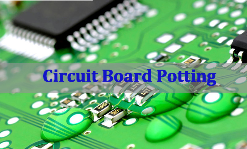
Circuit board potting is a critical encapsulation process in electronics manufacturing where a liquid compound is poured or dispensed over an assembled PCB (PCBA) and cured to form a solid, protective shell. This comprehensive guide explores the advanced materials, methods, and design considerations for potting printed circuit boards to ensure maximum reliability in demanding applications.
Ensuring long-term protection for PCB assemblies is challenging, and many products fail not because of design flaws, but due to inadequate circuit board potting strategies.
- Premature Field Failures
Moisture, vibration, and thermal cycling quickly degrade unprotected PCBs. - Material Selection Confusion
Epoxy, silicone, or urethane—choosing the wrong compound risks performance and reliability. - Process-Induced Defects
Air entrapment, voids, and cure stress compromise protection and component integrity. - No Path for Repair or Rework
Poor potting decisions turn minor failures into full board scrap. - Added Weight and Cost
Excessive potting weight on circuit boards impacts both BOM and product specs.
These challenges can be overcome by treating circuit board potting as an engineered PCBA process—not a material-only decision.
- Engineered Reliability
Potting systems are designed to match real thermal, mechanical, and environmental loads. - Scientific Material Selection
The right epoxy resin circuit board potting compound is chosen based on data, not assumptions. - Controlled, Validated Processes
Degassing, precision dispensing, and controlled curing eliminate voids and stress. - Design for Serviceability
Where required, repairing potted circuit board assemblies remains feasible. - Optimized Weight and Cost
Potting volume and geometry are engineered to protect—without unnecessary mass or expense.
At EBest Circuit (Best Technology), we specialize in transforming vulnerable electronic assemblies into ruggedized, reliable products. We are not just a PCBA manufacturer; we are your solution partner for advanced circuit board potting and encapsulation. Our engineers combine deep material science knowledge with state-of-the-art process controls to deliver potted assemblies that excel in the harshest environments. If you have any PCB inquiries, pls feel free to contact our engineering team at sales@bestpcbs.com.
What Is Circuit Board Potting in Printed Circuit Board Manufacturing?
Circuit board potting is a foundational protection process in electronics manufacturing. It involves completely enveloping a PCB assembly (PCBA) in a liquid resin that subsequently cures into a solid, monolithic block. This section defines the process, its objectives, and its place in the manufacturing workflow.
- Core Objective: To provide a hermetic or near-hermic seal against environmental and operational threats.
- Primary Threats Mitigated:
- Environmental: Moisture, humidity, dust, debris, and corrosive gases.
- Mechanical: Shock, vibration, and physical impact.
- Electrical: Prevention of arcing, corona, and short circuits in high-voltage applications.
- Chemical: Resistance to fuels, solvents, oils, and cleaning agents.
- Process Placement: Typically a final manufacturing step after full PCBA testing, though sometimes done in stages for complex assemblies.
Unlike a surface-level conformal coat, potting fills all cavities and crevices, providing bulk, structural reinforcement and superior stress distribution. The result is a potted circuit board that behaves as a single, robust unit, significantly enhancing its operational lifespan in challenging conditions.
What Makes a Potted Circuit Board Different From an Unprotected PCBA?
Choosing between a potted board and an unprotected assembly is a fundamental design decision that directly impacts reliability, serviceability, and long-term performance in real-world environments.
| Feature | Unprotected PCBA | Potted Circuit Board |
|---|---|---|
| Environmental Protection | None | Fully sealed |
| Mechanical Robustness | Low | High |
| Thermal Behavior | Air-dependent | Compound-influenced |
| Electrical Insulation | Limited | High dielectric strength |
| Repair & Rework | Easy | Very difficult |
| Weight & Volume | Minimal | Increased |
An unprotected PCBA prioritizes accessibility, flexibility, and ease of debugging, making it suitable for controlled environments or products that require frequent servicing. In contrast, a potted circuit board fundamentally changes how the assembly behaves once deployed.
By encapsulating components in a solid compound, potting dramatically improves resistance to moisture, vibration, and electrical stress, while simultaneously limiting access for inspection, testing, or repair. Thermal performance also shifts from air-based cooling to conduction through the potting material, requiring careful compound selection and layout planning.
In short, potting a circuit board trades serviceability for survivability. The right choice depends on how harsh the operating environment is, how long the product must last without intervention, and whether field repair is a realistic requirement.
Why Do Engineers Choose Potting Circuit Boards for Harsh Operating Environments?
Engineers specify potting printed circuit boards when the application’s survival depends on maximum defense. It is the go-to solution for electronics that must operate reliably where other protections fail.
- Outdoor & Automotive Electronics: Under-the-hood control units, LED drivers, and sensors face temperature extremes, condensation, and salt spray.
- Industrial & Drivetrain Systems: Motor drives, power supplies, and controllers in factories withstand constant vibration, metal shavings, and coolant mists.
- Marine & Submersible Devices: Navigation and sensing equipment requires a complete, high-pressure moisture barrier.
- Aerospace & Defense Avionics: Systems must survive extreme G-forces, wide thermal cycling, and high-altitude conditions.
- High-Voltage/Power Electronics: Potting prevents arcing, reduces corona discharge, and manages partial discharge, which is critical for longevity.
- Consumer Durables: High-end tools, outdoor appliances, and wearables use potting for ruggedization and water resistance.
The choice for potting circuit boards is driven by a risk assessment: the consequences of field failure (cost, safety, reputation) far outweigh the added manufacturing complexity and cost of potting.
How Do You Select the Right Circuit Board Potting Material for Electronic Assemblies?
Selecting a circuit board potting compound is a multi-variable optimization problem. The ideal material balances protection with compatibility. The core question is rarely “will any epoxy work as circuit board potting?” but rather “which system provides the optimal property set?”
- Define the Environmental Stressors: List all threats: operating temperature range, thermal cycling magnitude, chemical exposure, vibration spectrum, and required ingress protection (IP rating).
- Understand Material Families:
- Epoxies: High strength, good adhesion, excellent chemical resistance. Can be rigid, leading to component stress during thermal cycling.
- Silicones: Extremely flexible, wide temperature range, good electrical properties. Lower mechanical strength and often higher cost.
- Polyurethanes: A balance of flexibility, toughness, and good moisture resistance. Can be sensitive to moisture during curing.
- Match Key Properties: Compare the candidate materials’ datasheets against your needs:
- Coefficient of Thermal Expansion (CTE): Should match components/board to minimize stress.
- Glass Transition Temperature (Tg): For epoxies, ensure operating temperature is below Tg or the compound becomes soft.
- Modulus of Elasticity: A measure of stiffness (high modulus) vs. flexibility (low modulus).
- Dielectric Strength & Constant: Critical for high-voltage or high-frequency boards.
- Consider the Process: Assess pot life, mix ratio, viscosity, and cure schedule. A low-viscosity material flows better around dense components.
- Evaluate Secondary Needs: Is optical clarity needed? Is UL94 V-0 flame retardancy required? Is repairing potted circuit board a future need (hinting at a reworkable silicone)?
For instance, a high-vibration automotive application might choose a flexible urethane, while a stable, high-heat power module might use a filled, thermally conductive epoxy.
When Is Epoxy Resin Circuit Board Potting the Preferred Encapsulation Method?
Epoxy resin circuit board potting is the workhorse of rigid encapsulation, chosen when the priority is creating a hard, fortress-like shell. It is not a universal solution but excels in specific scenarios.
- When Maximum Mechanical Rigidity is Needed: For PCBs that are structural members or must resist high, constant mechanical loads.
- For Superior Chemical Resistance: When exposed to aggressive solvents, fuels, or acids where other compounds might swell or degrade.
- In High-Temperature, Static Environments: If the operating temperature is high but stable (minimal cycling), and is below the epoxy’s Tg. Epoxies can have a higher continuous use temperature than many urethanes.
- For Excellent Adhesion to Diverse Substrates: Epoxy bonds tenaciously to metals, most plastics, and the PCB itself, preventing moisture ingress at interfaces.
- When Cost-Effectiveness is Key: Epoxy systems are often more economical per volume than specialty silicones or urethanes.
- For High Thermal Conductivity (When Filled): Loaded with ceramic or other fillers, epoxy resin circuit board potting compound can effectively move heat away from components, acting as a heatsink.
However, its rigidity is a double-edged sword. In applications with severe thermal cycling, the mismatch in CTE between the rigid epoxy and components can exert tremendous stress, potentially fracturing solder joints or the components themselves. This is a key decision point between epoxy and more flexible compounds.
How Does Potting a Circuit Board Impact Mechanical Strength and Thermal Behavior?
Potting a circuit board fundamentally alters its mechanical and thermal response. The compound doesn’t just add a layer; it couples all elements together, changing the system’s dynamics.
- Mechanical Reinforcement:
- Vibration Damping: The potting compound, especially flexible ones, absorbs vibrational energy, reducing the amplitude of oscillations transmitted to components. The damping effect can be modeled, but practically, it prevents solder fatigue.
- Impact Resistance: The mass distributes a point impact load across the entire assembly, protecting fragile components. The compound’s toughness (ability to absorb energy) is critical here.
- Stress on Components: A high-modulus (rigid) compound can transfer board flexure stresses directly to component leads. A low-modulus (flexible) compound allows for relative strain, reducing stress.
- Thermal Management Redefinition:
- From Convection to Conduction: Potting eliminates air flow. Heat must now be conducted through the compound to the outer casing. This makes the thermal conductivity (k) of the potting material a critical parameter.
- The Thermal Path: The effectiveness depends on the compound’s ‘k’ value and the potting thickness on circuit boards. The thermal resistance (Rθ) of the potting layer is Rθ= thickness / (k * area). A thicker layer of a low-k material is a significant insulator.
- System-Level Consideration: Design must ensure a clear conductive path from the heat-generating component, through the compound, to the enclosure or heatsink. Thermal interface materials (TIMs) or direct component bonding may be needed.
In summary, potting turns a collection of parts into a composite material. Its mechanical and thermal properties are now a weighted average of the PCB, components, and the potting compound itself.
What Design and Process Factors Matter When Using Circuit Board Potting Compound?
Successfully potting printed circuit boards requires forethought in both design and process. Ignoring these factors can lead to failure.
- Design for Potting (DfP) Considerations:
- Component Selection & Layout: Avoid components that can’t be potted (e.g., potentiometers, relays that need access). Orient tall components to facilitate compound flow. Create “flow channels” on the board.
- Stress Relief: Use flexible glob-top or underfill for large BGAs or QFNs before global potting to mitigate CTE mismatch stress.
- Venting and Filling: Design the enclosure with a fill port at the lowest point and a vent at the highest to ensure complete, bubble-free filling.
- Potting Damns & Barriers: Use temporary or permanent dams to contain compound to specific areas if full-board potting isn’t required.
- Material Compatibility: Verify that the compound is compatible with all component coatings, connectors, wire insulations, and the PCB solder mask.
- Critical Process Controls:
- Pre-Conditioning: Bake the assembly to remove moisture that could cause voids (“pop-corning”) during cure.
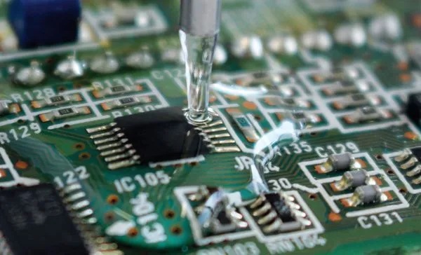
- Mixing & Degassing: Precisely mix multi-part compounds and degas the mixture under vacuum to remove entrained air before dispensing.
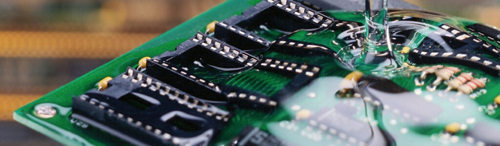
- Dispensing Technique: Use a controlled, slow pour or automated dispensing to allow the compound to flow and minimize air entrapment. Pour in a thin stream at the lowest point.
- Cure Profile: Follow the manufacturer’s recommended time and temperature profile. Ramping the temperature too quickly can cause excessive exotherm and stress.
- Inspection: Use ultrasonic scanning or X-ray to inspect for hidden voids or delamination in critical assemblies.
A well-designed board with a poorly controlled process (or vice-versa) will likely result in a defective potted circuit board.
Is Repairing Potted Circuit Board Possible in Production or Field Service?
The question of repairing potted circuit board assemblies is complex. The short answer is: it is often difficult, sometimes possible, and always expensive. Potting is designed to be permanent, and remove potting from circuit board is a destructive, high-risk procedure.
- The Challenge of De-potting: The process to remove potted circuit board encapsulation is invasive. It often involves:
- Mechanical Milling: Precise CNC milling to the component level, risking collateral damage.
- Thermal Methods: Heating the entire assembly to the compound’s decomposition point, which can destroy all components.
- Chemical Solvents: Using aggressive, heated solvents (e.g., nitric acid for epoxy) that can attack board laminates and components. This is a last-resort lab procedure, not a field service operation.
- Designing for Serviceability:
- Use of Reworkable Compounds: Some silicone potting circuit board applications or specialized urethanes are softer and can be cut and peeled away more easily, though it remains messy.
- Modular/Compartmentalized Design: Pot only the sub-assembly that requires protection (e.g., the high-voltage section) and leave the control/logic section accessible in a separate compartment.
- Connectors Over Direct Solder: Use connectors between potted and non-potted modules, allowing a faulty potted module to be replaced entirely.
In production, a failed board post-potting is almost always scrapped. In the field, the economics typically favor module replacement over attempting a de-potting circuit board and repair. Therefore, the decision to pot must be made with the understanding that the assembly is essentially rendered unserviceable.
To conclude, circuit board potting is a powerful transformative process that elevates a standard PCBA into a hardened, environmentally sealed device capable of surviving conditions that would defeat lesser protections. This guide has detailed the critical considerations, from material science and mechanical impacts to design and process controls, that define successful potting.
Mastering advanced potting is not about simply filling a box with resin; it is the strategic integration of material properties, mechanical design, and precise manufacturing to solve reliability challenges. It moves beyond the question of “how to pot a circuit board” to “how to design a system where potting ensures flawless, long-term operation.”
At EBEST CIRCUIT (Best Technology), this strategic mastery is applied directly to every customer project.
EBEST CIRCUIT (Best Technology) analyzes stress profiles, selects the optimal compound—whether a rugged epoxy resin circuit board potting system or a flexible silicone—and applies controlled, repeatable processes to ensure each potted circuit board meets defined reliability targets. For a consultation on your next PCB or PCBA project, pls feel free to contact us at sales@bestpcbs.com.