

Copper thickness is a key factor that affects how your board performs. Choosing the right copper thickness is an important part of PCB design, it affects how well your circuit works, how long it lasts, and even how much it costs. In this blog, we’ll break down why copper thickness matters, how to pick the right option for your PCB design—— to help you make informed decisions for your next project.
Why Copper Thickness Matters?
1. Current Carrying Capacity
Thicker copper layers handle higher currents without overheating. For example:
- 1 oz copper: Supports up to ~3A per 10mm trace width.
- 2 oz copper: Doubles the capacity to ~6A for the same width.
- Critical for power circuits like motor controllers or LED drivers.
- 3 oz+ Copper (140µm+):
- Handles 12A+ per 10mm, suited for extreme applications like inverters or industrial power supplies. However, thicker copper increases fabrication costs and requires specialized manufacturing.
2. Signal Integrity
High-frequency designs (e.g., RF, 5G): Thinner copper (0.5 oz–1 oz) with smooth surfaces reduces signal loss.
Standard circuits: 1 oz copper is sufficient for most low-frequency applications.
3. Durability
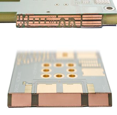
Thicker copper (≥2 oz) withstands thermal stress during soldering and mechanical wear in harsh environments.
Thin copper (0.5 oz) may crack under repeated vibration or temperature changes.
4. Cost Efficiency
Thicker copper increases material costs and requires longer etching times.
Over-specifying thickness wastes money; under-specifying risks failure.
How to Choose the Right Thickness for Your PCB?
Based on our 19+years experiences in the PCB manufacturing field, today I would like to share you 6 Strategies How to Choose the Right Thickness
1. Calculate Current Requirements
Use the IPC-2152 standard or online tools (e.g., Saturn PCB Toolkit) to determine the minimum trace width and copper weight for your current.
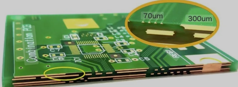
Example: A 5A power trace with 1 oz copper needs a 2mm width. With 2 oz copper, the width drops to 1mm, saving space.
2. Prioritize Space vs. Performance
High-density designs: Use thinner copper (0.5 oz–1 oz) to fit more traces.
Power-heavy boards: Option for 2 oz–6 oz copper to reduce trace widths and avoid overheating.
3. Factor in Manufacturing Limits
Thin copper (0.5 oz): Prone to over-etching; requires tighter process control.
Thick copper (>3 oz): Needs specialized plating and etching, increasing lead time and cost.
Common Mistakes to Avoid
- Ignoring Current Density: Thin traces with high current cause burnout.
- Over-Designing: Using 3 oz copper for low-power signals wastes space and money.
- Neglecting Manufacturer Feedback: Always confirm your fab house’s capabilities (e.g., max/min copper weight).
Conclusion
Choosing the right copper thickness balances performance, cost, and manufacturability. By aligning your design’s needs with industry standards and manufacturer capabilities, you can avoid costly redesigns and ensure long-term reliability.
Also, if you have more questions about PCB copper thickness or need help with your design, feel free to reach out to a send an inquiry. we’ll help you optimize copper thickness and maximize your board’s potential.