

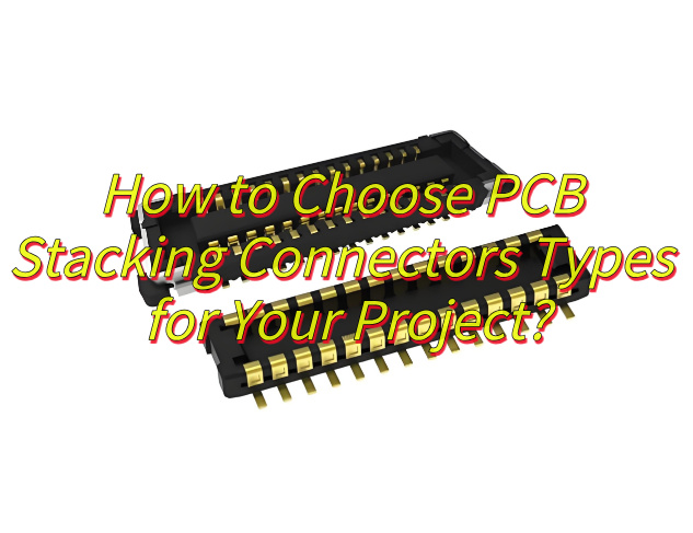
Are you worried about how to choose PCB stacking connectors for your project? This guide explore type selection tips, application, features, stack height for PCB stacking connectors.
- How to choose a stacking connector compatible with 5G/6G high-frequency signals?
- Why do my stacking connectors frequently fail in a vibration environment?
- How to control connector procurement costs under the demand for small batches and multiple varieties?
- From design to mass production, can you find a one-stop stacking interconnect solution?
EBest Circuit (Best Technology) Can Provide:
- 5G/6G high-frequency collaborative design service: provide impedance matching simulation report (10-100GHz), free output selection guide.
- Industrial-grade vibration reinforcement solution: vibration test data sharing (passed 20G/2000 hours test), failure analysis service.
- PCBA+SMT service: support 01005 component mounting, realize synchronous thermal management optimization of connectors and PCBs.
- One-stop solution: from DFM inspection to mass delivery, 24-hour rapid prototyping, 15-day mass production cycle.
Welcome to contact EBest Circuit (Best Technology) if you have any inquiry for PCBA or SMT service: sales@bestpcbs.com.
What Are PCB Stacking Connectors?
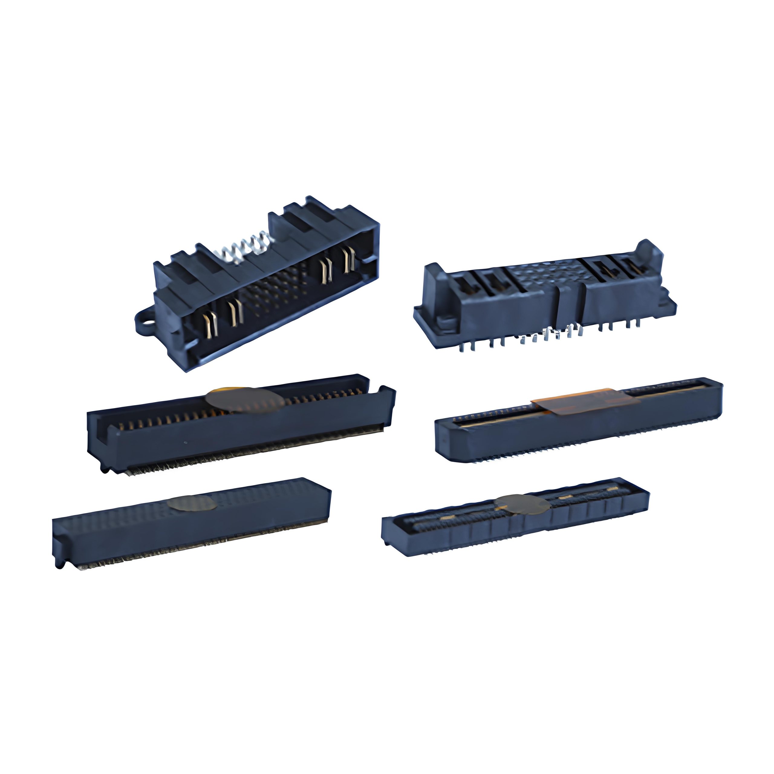
PCB stacking connectors are specialized interconnect components designed for vertically stacking multiple printed circuit boards (PCBs) to save space in compact electronic devices. They establish electrical pathways between layers while maintaining structural integrity, integrating signal pins for data transfer alongside dedicated power and ground contacts for stable current distribution.
These connectors feature precise alignment mechanisms to ensure reliable mating across stacked layers, often supporting differential pairs for high-speed protocols like PCIe or USB. Their design incorporates impedance-matched layouts to minimize signal reflections and electromagnetic interference (EMI). Mechanical stability is enhanced through locking features that prevent disconnection under vibration, with contact materials selected for durability across temperature variations. Selection depends on parameters such as stacking height adjustability, pin pitch density, and current-carrying capacity.
How to Choose PCB Stacking Connectors Types?
Methods about how to choose PCB stacking connectors types for your project:
1.Flexible Stacking Connectors
- Application: Used in scenarios requiring bending or dynamic connections, such as foldable devices (e.g., laptop hinges), medical wearables, or robotic joints.
- Selection Advice: Prioritize for low-hardness silicone or polyimide substrates to maintain signal integrity after repeated bending. Verify the minimum bending radius to avoid stress-induced damage.
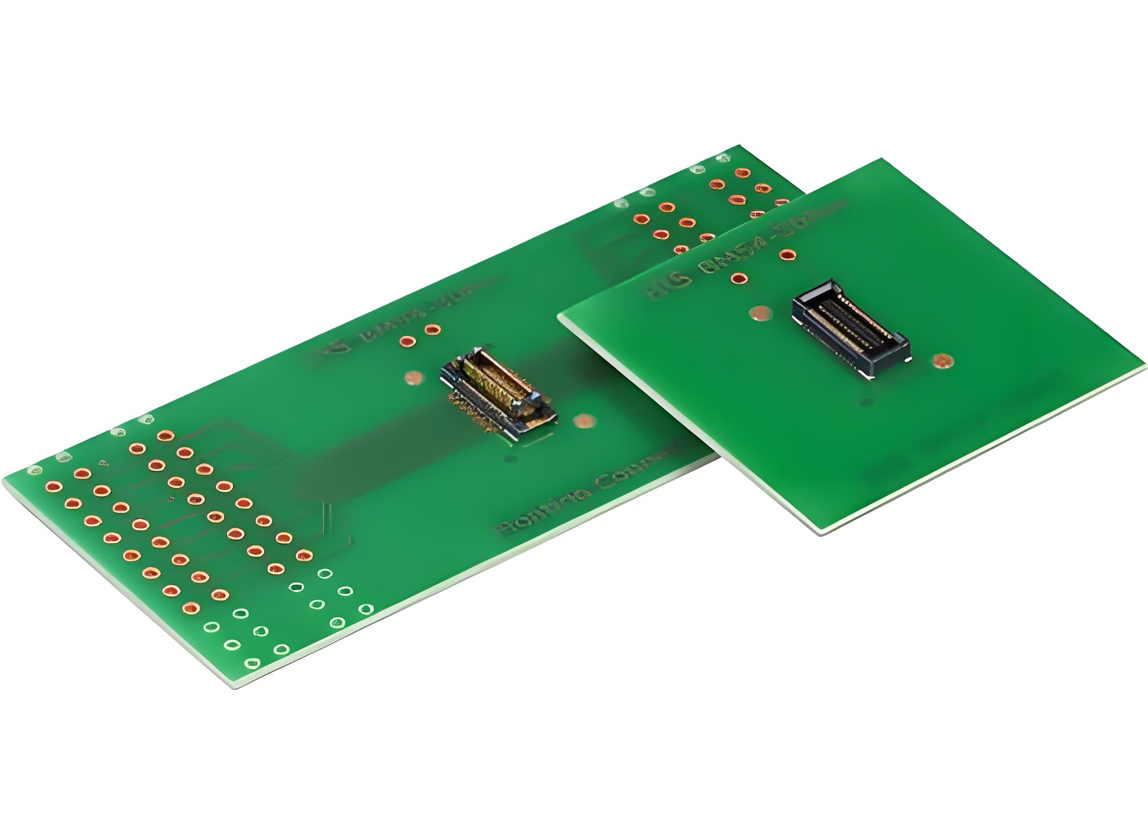
2.Mezzanine Connectors
- Application: Suitable for compact stacking designs like single-board computers (SBC), communication base station modules, or vertical interconnections between consumer electronics motherboards and daughterboards.
- Selection Advice: Focus on pin density (e.g., 0.5mm/0.8mm pitch) and impedance control. For high-frequency applications, select models with differential pair layouts. Surface-mount (SMT) types are recommended for automated assembly.
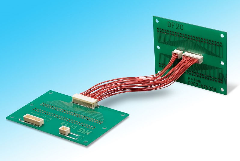
3.Board-to-Board Connectors (Vertical/Horizontal)
- Application: Vertical types save horizontal space (e.g., IoT modules), while horizontal types suit short-distance connections between parallel boards (e.g., power modules and control boards).
- Selection Advice: For vertical connectors, validate insertion/extraction force and durability. For horizontal types, ensure pin pitch and creepage distance comply with high-voltage safety standards.
3.Coaxial Stacking Connectors
- Application: Designed for RF or microwave signal transmission in 5G communication devices, radar systems, or satellite communication modules.
- Selection Advice: Choose 50Ω or 75Ω impedance-matched models. Evaluate insertion loss and return loss parameters. Ensure outer conductor grounding aligns with PCB ground plane design.
4.High-Current Stacking Connectors
- Application: Used in power distribution networks (PDN) for electric vehicle battery management systems (BMS), industrial motor controls, or high-power LED driver boards.
- Selection Advice: Assess per-pin current capacity (e.g., >10A/pin). Select copper alloy materials with silver plating. Consider thermal management paths and supplement with thermal interface materials if necessary.
5.Low-Profile Stacking Connectors
- Application: Perfect for ultra-thin devices (e.g., smartphones, tablets) or space-constrained stacking scenarios.
- Selection Advice: Prioritize ZIF (Zero Insertion Force) or LIF (Low Insertion Force) designs. Select models with a height below 1.5mm. Verify pin coplanarity tolerance to avoid soldering defects.
4.Hermetic Stacking Connectors
- Application: Suitable for extreme environments (e.g., aerospace, deep-sea exploration) or applications requiring air/water-tight protection.
- Selection Advice: Use glass-to-metal seal (GTMS) or ceramic packaging. Validate certifications like IP68 or MIL-STD-810. Ensure sealing materials are compatible with operational temperature ranges.
5. Modular Stacking Connectors
- Application: Ideal for scalable systems like test/measurement equipment, configurable industrial controllers, or educational experiment platforms.
- Selection Advice: Choose modular interfaces supporting hot-swapping. Focus on programmable pin definitions. Reserve redundant pins for future functional upgrades.
6.Optical Stacking Connectors
- Application: Used for high-speed optical signal transmission in data center optical modules, fiber communication devices, or LiDAR systems.
- Selection Advice: Select MPO/MTP multi-fiber connectors or expanded beam designs. Evaluate insertion loss and return loss. Ensure alignment accuracy and dust-proof protection.
7.Low-Profile Stacking Connectors
- Application: Perfect for ultra-thin devices (e.g., smartphones, tablets) or space-constrained stacking scenarios.
- Selection Advice: Prioritize ZIF (Zero Insertion Force) or LIF (Low Insertion Force) designs. Select models with a height below 1.5mm. Verify pin coplanarity tolerance to avoid soldering defects.
8.Hermetic Stacking Connectors
- Application: Suitable for extreme environments (e.g., aerospace, deep-sea exploration) or applications requiring air/water-tight protection.
- Selection Advice: Use glass-to-metal seal (GTMS) or ceramic packaging. Validate certifications like IP68 or MIL-STD-810. Ensure sealing materials are compatible with operational temperature ranges.
9.Modular Stacking Connectors
- Application: Ideal for scalable systems like test/measurement equipment, configurable industrial controllers, or educational experiment platforms.
- Selection Advice: Choose modular interfaces supporting hot-swapping. Focus on programmable pin definitions. Reserve redundant pins for future functional upgrades.
10. Optical Stacking Connectors
- Application: Used for high-speed optical signal transmission in data center optical modules, fiber communication devices, or LiDAR systems.
- Selection Advice: Select MPO/MTP multi-fiber connectors or expanded beam designs. Evaluate insertion loss and return loss. Ensure alignment accuracy and dust-proof protection.
What Are Features of PCB Stacking Connectors?
Features of PCB Stacking Connectors:
- Space-saving design: Allows tight board stacking for compact devices.
- High-speed support: Maintains signal integrity for PCIe/USB with impedance control.
- Power management: Dedicated power/ground pins ensure stable current flow.
- Mechanical reliability: Locking mechanisms prevent disconnection from vibration.
- Adjustable heights: Custom spacing options for thermal/routing needs.
- EMI protection: Shielding elements reduce interference in noisy environments.
Application of PCB Stack Connectors
- Consumer Electronics – Smartphone display-to-mainboard links, wearable device circuit stacking, laptop power distribution network.
- Telecommunications – 5G base station RF module connections, network switch backplane interfaces, satellite communication phased arrays.
- Industrial Automation – Robotics control system stacking, CNC machine signal transmission paths, power converter module interconnects.
- Automotive Systems – ADAS sensor cluster integration, EV battery management circuits, and infotainment system PCB assemblies.
- Medical Technology – Portable imaging equipment module stacking, patient monitoring signal routing, surgical instrument control interfaces.
- Aerospace & Defense – Avionics system ruggedized connections, radar array signal distribution networks, satellite payload module configurations.
What Is the Stack Height of Board-to-Board Connectors?
Stack height ranges for board-to-board connectors:
Standard Stack Height Options
- Ultra-Low Profile: 1.00–1.50 mm (0.039–0.059 inches) for space-constrained designs like wearables.
- Common Range: 3.00–8.00 mm (0.118–0.315 inches) suits consumer electronics and industrial controls.
- Extended Heights: 10.00–31.90 mm (0.394–1.255 inches) for modular systems requiring thermal or mechanical clearance.
Precision Increments
- Fine adjustments in 0.13 mm (0.005 inch) steps enable exact PCB alignment.
- Modular designs offer 1.00 mm (0.039 inch) incremental options between 5.00–16.00 mm.
Application-Specific Guidelines
- High-Density PCBs: ≤5.00 mm heights with 0.4–0.8 mm pitch connectors optimize signal integrity.
- Vibration-Prone Systems: ≥6.00 mm heights improve mechanical stability.
- Power Modules: ≥10.00 mm heights accommodate heat dissipation.
Industry Standards
- Stack heights correlate with connector pitch (e.g., 0.8 mm pitch pairs with 5–16 mm heights).
- MIL-STD compliance ensures vibration resistance for critical environments.
- How to Align PCB Stack Connector Precisely in High Density Multilayer PCB Boards?
- Precision Alignment Techniques for PCB Stack Connectors in High-Density Multilayer Boards
How to Align PCB Stack Connector Precisely in High Density Multilayer PCB Boards?
Here’s a practical guide for precise stack connector alignment in high-density multilayer PCBs:
Design Phase Preparation
- Use identical reference points on all layers (0.1mm diameter).
- Maintain consistent layer-to-layer registration marks.
- Implement 3:1 aspect ratio for via-to-pad connections.
Fabrication Controls
- Require laser direct imaging (LDI) for layer patterning.
- Specify ±25μm layer-to-layer alignment tolerance.
- Verify optical targets with automated inspection systems.
Material Selection
- Choose low-Dk materials with stable thermal properties.
- Use matching CTE cores and prepregs.
- Select laminates with <0.2% dimensional change after lamination.
Process Techniques
- Apply sequential lamination with intermediate inspections.
- Utilize pinless registration systems for multilayer builds.
- Implement controlled ramp rates during pressing cycles.
Verification Methods
- Perform cross-section analysis on test coupons.
- Conduct microsection evaluation of actual connectors.
- Use X-ray inspection for hidden layer verification.
Troubleshooting Tips
- Measure skew between top/bottom layers first.
- Check for resin flow variations in pressed boards.
- Verify drill wander doesn’t exceed 50μm per 100μm depth.
EBest Circuit (Best Technology) Board-to-Board Connector Examples
If you have any request for board to board connectors, welcome to contact EBest Circuit (Best Technology): sales@bestpcbs.com. Looking forward to hearing from you!