

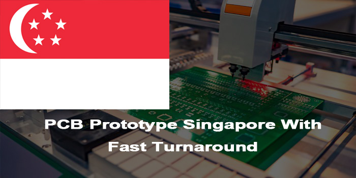
High-quality PCB prototype Singapore is key to streamlining R&D workflows and shortening product development cycles in Singapore’s advanced electronics sector. Our solutions deliver dependable Singapore PCB prototype services, backed by rigorous quality oversight and swift turnaround, directly addressing the core demands of local projects from initial design validation to small-batch production readiness.
Are You Facing These Problems of PCB Prototype Singapore?
- Do you face inaccurate prototyping that leads to repeated rework and delayed timelines for your PCB projects in Singapore?
- Is the minimum order quantity for your prototype PCBs set too high, unnecessarily driving up your R&D costs in Singapore?
- Does lack of professional DFM analysis cause soldering defects in your Singapore PCB prototype?
- Can you barely find suppliers that handle specialized boards like ceramic or HDI for your prototyping needs in Singapore?
- Do delivery delays of PCB prototype assembly Singapore disrupt your follow-up production plans?
- Is the prototyping quality inconsistent without clear certification support for your Singapore-based PCB projects?
- Can you not track the real-time production progress of your prototype PCB Singapore?
- Do you struggle with signal integrity issues in high-end prototypes due to inadequate impedance control for PCB prototype Singapore?
PCB Prototyping Singapore: Full Process From Demand to Delivery
We deliver end-to-end support for PCB prototype Singapore, spanning from initial demand alignment to final product delivery. Our team starts with in-depth technical consultation to clarify parameters like layer count, impedance requirements, and material specifications, ensuring every detail aligns with your project goals.
Free professional DFM (Design for Manufacturing) optimization is a core part of our service. We combine advanced software tools and 19 years of engineering experience to scan designs for potential flaws, such as inadequate trace spacing, improper pad layout, or manufacturability issues, reducing rework risks and shortening development cycles.
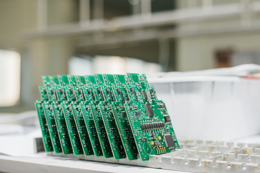
Production is backed by high-grade materials and precision processes, with multi-stage inspection nodes to uphold quality. From raw material verification to X-ray inspection and electrical testing, each step adheres to strict industry standards, ensuring consistency for your Singapore PCB prototype.
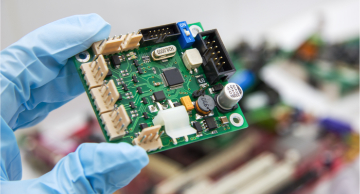
For PCB prototype assembly Singapore, we offer one-stop solutions integrating component sourcing, SMT/THT assembly, and functional testing. Our precise soldering capabilities (including BGA/QFN) deliver ready-to-test products, while real-time progress updates via MES system keep you informed, ensuring full transparency throughout the process.
Why Choose EBest(Best Technology) for PCB Prototype Singapore?
Reasons Why Choose EBest(Best Technology) for PCB Prototype Singapore:
- 24-Hour Expedited Prototyping: Deliver standard 2-4 layer prototypes within 24 hours, boasting a 99% on-time delivery rate to meet urgent project deadlines in Singapore.
- 19 Years of Industry Expertise: With nearly two decades of focus on PCB prototyping in Singapore, we master regional market demands and complex manufacturing processes for stable quality.
- Advanced Process Capabilities: Manufacture ceramic PCBs and HDI boards with 0.1mm minimum blind/buried vias, supporting high-end prototype PCB Singapore requirements for medical and aerospace fields.
- Strict Quality Certifications: Hold ISO9001, AS9100D, and IATF 16949 certifications, ensuring products meet medical, automotive, and aerospace-grade standards for Singapore PCB prototype projects.
- One-Stop PCBA Solutions: Integrate PCB prototype assembly Singapore with component sourcing, SMT/THT assembly, and functional testing for seamless project progression from design to validation.
- Full Production Traceability: Equipped with MES system to track every step of production, providing complete data records for quality verification and compliance of PCB prototype Singapore.
- Localized Rapid Response: Maintain a dedicated support team for Singapore clients, offering 2-hour response to inquiries and on-demand technical consultations to resolve issues promptly.
- Flexible Low-Volume Support: No minimum order quantity, enabling cost-effective 1-piece prototyping with optimized material paneling to reduce R&D costs for local projects.
- Free DFM Optimization: Provide professional Design for Manufacturing analysis to eliminate potential flaws, reducing rework rates by over 40% for PCB prototype Singapore orders.
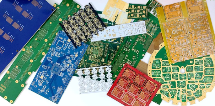
Types of Singapore PCB Prototyping Service We Can Offer
- Rigid PCB Prototyping: Supports 1-64 layers with 0.075mm (3mil) minimum line width/spacing, using high-grade FR-4 substrate. Offers precise impedance control for industrial control, consumer electronics and automotive components.
- Flexible & Rigid-Flex PCB Prototyping: Adopts polyimide materials (bend radius ≤1mm, -40℃ to 125℃ operating temp) for wearables, compact medical tools and aerospace use, with durability over 10,000 bending cycles.
- HDI PCB Prototyping: Features 0.05mm laser-drilled microvias and 4-24 layer blind/buried hole design, optimized for high-speed signals in 5G base stations, industrial controllers and precision medical equipment.
- Ceramic PCB Prototyping: Delivers ≥200 W/(m·K) thermal conductivity for high-power and medical devices, complying with medical standards for harsh environments in PCB prototype Singapore.
- PCB Prototype Assembly Singapore: One-stop SMT/THT assembly (BGA/QFN, 01005 components) with AOI detection and 100% ICT/FCT testing, plus component sourcing with alternatives for parts shortages.
Our PCB Manufacturing Capabilities
| Item | Capabilities |
| Layer Count | 1 – 32 Layers |
| Max Board Dimension | 2424″ (610610mm) |
| Min Board Thickness | 0.15mm |
| Max Board Thickness | 6.0mm – 8.0mm |
| Copper Thickness | Outer Layer: 1oz~30oz, Inner Layer: 0.5oz~30oz |
| Min Line Width/Line Space | Normal: 4/4mil (0.10mm); HDI: 3/3mil (0.076mm) |
| Min Hole Diameter | Normal: 8mil (0.20mm); HDI: 4mil (0.10mm) |
| Min Punch Hole Dia | 0.1″ (2.5mm) |
| Min Hole Spacing | 12mil (0.3mm) |
| Min PAD Ring(Single) | 3mil (0.075mm) |
| PTH Wall Thickness | Normal: 0.59mil (15um); HDI: 0.48mil (12um) |
| Min Solder PAD Dia | Normal: 14mil (0.35mm); HDI: 10mil (0.25mm) |
| Min Soldermask Bridge | Normal: 8mil (0.2mm); HDI: 6mil (0.15mm) |
| Min BAG PAD Margin | 5mil (0.125mm) |
| PTH/NPTH Dia Tolerance | PTH: ±3mil (0.075mm); NPTH: ±2mil (0.05mm) |
| Hole Position Deviation | ±2mil (0.05mm) |
| Outline Tolerance | CNC: ±6mil (0.15mm); Die Punch: ±4mil (0.1mm); Precision Die: ±2mil (0.05mm) |
| Impedance Controlled | Value>50ohm: ±10%; Value≤50ohm: ±5ohm |
| Max Aspect Ratio | 0.334027778 |
| Surface Treatment | ENIG, Flash Gold, Hard Gold Finger, Gold Plating(50mil), Gold finger, Selected Gold plating, ENEPIG, ENIPIG; HAL, HASL(LF), OSP, Silver Immersion, Tin Immersion |
| Soldermask Color | Green/White/Black/Yellow/Blue/Red |
Our Lead Time for Prototype PCB Prototype
| Layers | Normal Service | Fastest Service |
| 1 | 7 Days | 24 H |
| 2 | 8 Days | 24 H |
| 4 | 10 Days | 48 H |
| 6 | 10 Days | 72 H |
| 8 | 12 Days | 72 H |
| ≥10 | TBD | TBD |
Case Studies of Our Singapore PCB Prototype
Project Background: A local Singapore medical device manufacturer required PCB prototype Singapore for a portable patient monitor, targeting bedside clinical use with non-negotiable high reliability and medical industry compliance.
Project Requirements: 8-layer HDI PCB (to fit the device’s compact structure) with impedance control, full ISO 13485 medical standard compliance, and 30 prototypes delivered in 5 days for critical clinical trial validation.
Project Challenges: The 5-day timeline was extremely tight for HDI prototyping; the ±5% impedance tolerance far exceeded industry standard ±10%; low-noise design was mandatory to avoid interfering with vital sign signal collection.
Our Solutions: Activated dedicated expedited production lines; used laser drilling for 0.05mm microvias to meet HDI demands; conducted free DFM optimization (signal layer-ground isolation design) to enhance noise resistance; implemented triple inspections (X-ray for layer alignment, impedance testing, electrical performance verification) to eliminate defects.
Output Results: Delivered the prototype PCB Singapore 1 day ahead of schedule (4 days total), achieving a 99.8% yield rate with zero electrical or structural defects. The prototypes passed ISO 13485 audits, with signal noise controlled below 8μV to ensure accurate vital sign detection. The client recognized our precision and efficiency, and has since partnered with us for mass production of the monitor.
FAQs of PCB Prototyping in Singapore
Q1: Why does my PCB prototype Singapore have signal interference issues?
A1: This is often caused by improper trace layout or material selection. We solve it by conducting free signal integrity analysis for every prototype PCB Singapore order, optimizing trace spacing and layer stackup, and recommending suitable high-frequency materials if needed, reducing interference by over 90%.
Q2: How to avoid solder mask peeling on Singapore PCB prototype?
A2: Solder mask peeling stems from poor curing or low-quality materials. Our process uses UV-curable solder mask (10-25µm thickness) and precise temperature control during curing, with 100% visual inspection to ensure no peeling, meeting IPC standards.
Q3: Can I get PCB prototype Singapore with no minimum order quantity?
A3: Yes. We offer zero-MOQ PCB prototyping in Singapore, supporting orders from 1 piece. Through material panel optimization, we reduce per-piece costs by 35% for small-batch orders, ideal for R&D validation.
Q4: How to track the production progress of PCB prototype Singapore?
A4: We provide a dedicated MES system access for each order. You can real-time track every process node of PCB prototype Singapore, from material cutting to final inspection, with automatic progress notifications via email.
Q5: How to ensure compatibility between lead-free solder and components for Singapore PCB prototype?
A5: Lead-free solder (SnAgCu) has a higher melting point (245-260℃) than traditional solder, easily causing component damage or poor soldering. We conduct pre-production compatibility checks for all PCB prototype Singapore orders, match component pin materials with solder, optimize thermal expansion coefficient alignment, and select moisture-sensitive components with low-grade ratings, ensuring 99.5% soldering reliability and RoHS compliance.