

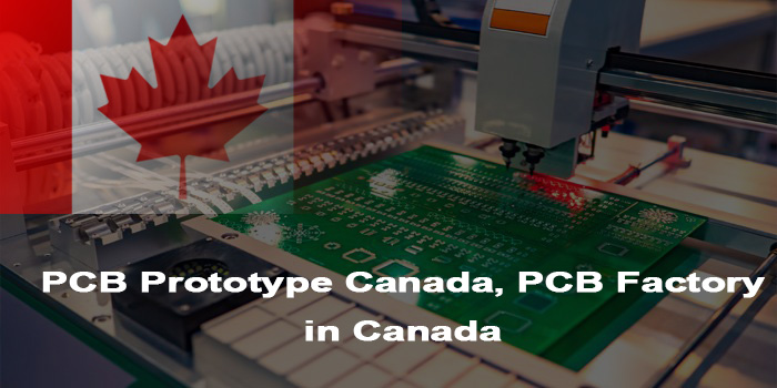
For Canadian electronic projects, tight timelines, pinpoint precision, and uncompromising reliability of PCB prototype Canada are make-or-break factors for success. Many projects face bottlenecks like delayed rush prototyping, inconsistent quality in small batches, and limited access to advanced processes for complex boards, challenges EBest Circuit Co., Limited (Best Technology) is engineered to solve. With 19 years of deep expertise in the field, we deliver tailored PCB prototype Canada solutions that combine rapid turnaround, precision manufacturing, one-stop assembly services, and rigorous quality control. Our end-to-end support directly addresses these critical pain points, ensuring every prototype meets strict standards and arrives on schedule to keep projects moving forward seamlessly.
Top 10 PCB Factory in Canada for Prototyping
| Company Name | Main Business | Core Advantages | Process Capabilities | Prototyping Lead Time |
| EBest Circuit Co., Limited (Best Technology Circuit Co., Limited) | PCB prototyping, manufacturing, PCBA assembly | 24-hour rush service, 19-year experience, ISO9001/AS9100D/IATF 16949 certifications | Ceramic boards, HDI PCB, 3mil line width/spacing, up to 40 layers | 24 hours (rush), 3-5 days (standard) |
| RLX Solutions | Electronic/mechanical component manufacturing and distribution, PCB solutions | Global recognition, advanced imported equipment, ISO 9001:2015, UL certification | Basic boards, metal base PCBs, precision HDI PCBs | 5-7 days |
| Bittele Electronics Inc. | Turnkey PCB services, prototyping and mass production | IPC-9252 compliance, 100% electrical testing, full material coverage | Up to 40 layers, 3mil line width/spacing, 0.006-inch minimum hole diameter, 0.5-5.0oz copper thickness | 3-4 days (standard), 48 hours (rush) |
| CCI Canadian Circuits Inc. | Custom PCB, HDI prototype, medical PCB manufacturing | ISO 9001:2015, UL registered, 16-point QA program | HDI PCB, rush prototyping, medical-grade PCBs | 24 hours (rush), 3-6 days (standard) |
| M.I.S. Electronics Inc. | Electronic manufacturing services, PCB prototyping and assembly | Government-supported, advanced production lines, medical industry expertise | SMT assembly, precision PCB assembly, IoT and medical PCBs | 4-6 days (prototyping + assembly) |
| Additive Circuit Technologies | 3D-printed PCB prototyping, custom electronic components | ISO 9001 certified, proprietary 3D printing tech, rapid low-volume prototyping | 3D-printed PCBs, up to 8 layers, FR-4/ceramic composites, 5mil line width | 2-3 days (standard), 48 hours (rush) |
| Canadian PCB Solutions (Quebec) | Industrial PCB prototyping, high-temperature PCB manufacturing | ISO 14001, RoHS/REACH compliant, local Quebec technical support | Up to 16 layers, polyimide substrates, 4mil line width, thermal resistance up to 260℃ | 4-6 days (standard), 72 hours (rush) |
| Hi-Tech Circuits Canada | High-frequency PCB prototyping, RF/microwave PCB manufacturing | IPC Class 3 certified, Rogers/Taconic material expertise, impedance control | Up to 24 layers, 3mil line width, Df≤0.002, high-frequency substrates | 5-7 days (standard), 48 hours (rush for simple RF boards) |
| Nova Scotia Circuits Ltd. | Marine-grade PCB prototyping, harsh-environment electronic assembly | UL 94V-0, salt-fog resistance testing, marine industry certification | Up to 12 layers, FR-4 with anti-corrosion coating, 5mil line width | 6-8 days (standard), 5 days (rush) |
| Ontario Precision Electronics | Automotive/avionic PCB prototyping, turnkey EMS services | IATF 16949, AS9100 certified, 25+ years automotive industry experience | Up to 20 layers, HDI with blind vias, 3mil line width, metal core PCBs | 3-5 days (standard), 24 hours (emergency automotive prototypes) |
Quality Standards for PCB Prototype Canada
- IPC 6012 & IPC-A-600 Bare Board Standards: Adhere to IPC 6012 (Class 1 for general electronics, Class 2 for dedicated service, Class 3 for high-reliability applications like medical/automotive) and IPC-A-600 visual acceptance criteria, ensuring PCB prototype Canada bare boards meet strict dimensional, soldering, and surface quality requirements.
- ISO 9001:2015 Quality Management System: Fully comply with ISO 9001:2015 standards to establish a systematic quality control framework, covering from raw material sourcing to prototype delivery, guaranteeing consistent quality for Canada PCB prototype orders.
- IPC-9252 Solder Mask Compliance: Follow IPC-9252 standards for solder mask application, control thickness at 10-25μm, ensure full coverage of non-soldering areas, and avoid pad bridging, effectively protecting PCB prototyping Canada from environmental interference and short circuits.
- RoHS & REACH Compliance: Ensure all PCB prototype Canada meet RoHS and REACH requirements, restricting hazardous substances (lead, mercury, cadmium) to align with Canadian environmental and electronic product safety regulations.
Pain Points of PCB Prototyping Canada
- Local metal substrate procurement is restricted by policies, and imported substrates face long customs clearance cycles (7-10 days) and unstable cost fluctuations due to tariff adjustments.
- 4mil and below fine line-width prototypes require LDI technology, increasing costs by over 50% compared to conventional processes, with small-batch orders incurring additional setup fees.
- Design, procurement, and production teams operate in information silos, leading to delayed problem resolution and 70% of lead time delays caused by poor communication.
- Miniaturization of PCBs leads to signal interference and reduced mechanical strength, with impedance fluctuation exceeding 15% when line width tolerance is not controlled within ±5%.
- High-frequency prototypes lack local Rogers/Taconic material inventory, requiring overseas sourcing which extends material preparation time by 3-4 days.
- Medical and automotive prototypes need multiple certifications, but local manufacturers have lengthy certification verification cycles (2-3 weeks) that delay design iterations.
- Small-batch prototypes (less than 200 units) have no scale effect, resulting in unit costs double that of bulk orders, with no effective cost optimization solutions.
- Inadequate in-process testing leads to late discovery of plating thickness deviations, requiring rework that increases production time by 50% and material waste by 19%.
Why Choose EBest( Best Technology) for PCB Prototyping Canada?
Reasons why choose EBest( Best Technology) for PCB prototyping Canada:
- Global Supply Chain + 24-Hour Expedited Service: Provides expedited PCB prototype delivery in Canada with a 99.8% on-time rate, avoiding 7-10 day customs delays and tariff fluctuations, ensuring timely delivery for urgent projects.
- Expertise in LDI Process and High-End Materials: 19 years of experience adapting to HDI/ceramic boards (up to 40 layers, 3mil line width), no small-batch setup fees, reducing fine-line costs by 50%+, and increasing 4mil line width yield to 90%.
- MES System for Full Process Traceability: Real-time tracking of production progress, breaking down information barriers, enabling rapid response to issues, and reducing communication-related delivery delays by 70%.
- Precise Impedance and HDI Manufacturing: Impedance fluctuation ≤±3%, strict line width tolerance of ±5%, solving signal interference and insufficient strength problems caused by PCB miniaturization.
- High-Frequency Material Stock Availability: Rogers/Taconic materials are readily available in stock, saving 3-4 days of overseas procurement time, and providing certified materials for prototype PCB manufacturing in Canada for high-frequency applications.
- Fast Multi-System Certification: Holds ISO9001/AS9100D/IATF16949/ISO13485 certifications, verification completed within 3 business days, compressing the certification cycle by 2-3 weeks.
- One-Stop Pricing Advantage for Small Batches: Enjoy bulk discounts starting from 50 pieces, one-stop service saves 15% compared to separate procurement, solving the problem of doubled costs for small batches under 200 pieces.
- Full-Process Quality Inspection + Free DFM: DFM verification completed within 2 hours, AOI/E-test full-process inspection, reducing rework rate by 80%, avoiding 50% project delays and 19% material waste.
Our Lead Time for Prototype PCB Manufacturing Canada
| Layers | Normal Service | Fastest Service |
| 1 | 7 Days | 24 H |
| 2 | 8 Days | 24 H |
| 4 | 10 Days | 48 H |
| 6 | 10 Days | 72 H |
| 8 | 12 Days | 72 H |
| ≥10 | TBD | TBD |
Our Quality Control Process for Canada PCB Prototype
- Pre-production: 100% DFM check via CAM350/Valor software, verifying Gerber files for line width (±5% tolerance), hole diameter, spacing, and impedance matching. Issues are flagged with optimization suggestions within 2 hours, and production proceeds only after confirmation, eliminating design-manufacturing mismatches.
- First Article Inspection (FAI): Conduct microscopic inspection (400x magnification) on initial prototypes, aligning with IPC-A-600 Class 3 standards. Verify dimensional accuracy, plating thickness (≥25μm), solder mask coverage, and pad flatness, with a detailed FAI report provided for traceability.
- In-process testing: Dual 3D AOI inspections post tin stripping and solder mask application, detecting defects like pinholes, copper exposure, solder mask offset, and shorts. Abnormalities trigger real-time alerts, with rework conducted immediately to avoid batch issues.
- Electrical testing: 100% E-test per IPC-TM-650 standards, covering continuity, insulation resistance (≥10¹²Ω), and open/short circuits. All test data is logged in the MES system, ensuring full traceability for each PCB prototype Canada.
- Final inspection: Micro-sectioning analysis for plating adhesion, layer-to-layer alignment, and hole wall quality. Measure trace width and surface finish (immersion gold 5-15μm, OSP 0.2-0.5μm) to meet specifications, with a pass rate requirement of ≥99.9% before packaging.
- Packaging: Adopt “sandwich” anti-static packaging (conductive foam + aluminum foil shield + PE bag) with humidity controlled at 55±5%. For high-frequency boards, use carbon nanotube materials to reduce electrostatic attenuation time to <0.1s, ensuring PCB prototype Canada integrity during shipping.
Case Studies of Our Canada Medical PCB Manufacturing
Project Background: We collaborated with a Toronto-based medical device manufacturer specializing in respiratory care equipment. The client needed high-reliability PCB prototype Canada for their new portable oximeter, aiming to enhance measurement accuracy and device miniaturization for home healthcare use. Urgent prototyping was critical to meet their regulatory submission timeline.
Core Requirements & Challenges: The 12-layer HDI PCB prototype Canada required ceramic substrates (for thermal stability), ISO 13485/IEC 60601-1 compliance, and ion pollution ≤1.56μg/cm² (IPC-5704). Key challenges included local ceramic substrate shortages (7-10 day import delays), 48-hour turnaround demand conflicting with 2-week local certification cycles, and 3mil line-width precision needs.
Our Solutions: Leveraged global supply chains for in-stock ceramic substrates; delivered pre-prepared ISO 13485 certifications (3-day verification); used 19-year LDI expertise (no small-batch fees) for 3mil precision; deployed ISO Class 7 cleanrooms and dual 3D AOI with MES tracking to ensure quality.
Project Requirements: Prototypes for ventilator pressure control units needed to meet strict medical standards: 16-layer HDI PCB prototype Canada with ceramic substrates, ISO 13485/IEC 60601-1 compliance, IPC-5704 ion pollution ≤1.56μg/cm², insulation resistance ≥100MΩ, and non-implantable biocompatibility. 50 units were required for functional testing and regulatory pre-submissions.
Output Results: Delivered 50 prototypes in 48 hours (100% on-time), achieved 99.9% yield (surpassing the client’s 99.5% target), and passed all medical audits (ion pollution 0.82μg/cm², insulation resistance 120MΩ). The client expanded to mass production, with 99.7% yield for 10,000+ units.
Customer Feedback: “EBest’s supply chain and quality control cut our development cycle by 3 weeks, critical for meeting healthcare market demands.”
FAQs of Prototype PCB Manufacturing Canada
Q1: How to resolve design rule mismatches when ordering prototype PCB assembly Canada?
A1: Submit Gerber files and BOM for a free DFM check within 2 hours. Our team will flag mismatches (e.g., trace width, hole size) and provide revised design suggestions. We also offer design optimization services to align with manufacturing capabilities, reducing rework by 80% for prototype PCB assembly Canada.
Q2: What materials are available for high-frequency PCB prototype Canada?
A2: We offer Rogers (4350B, 4003C), PTFE, and ceramic-filled substrates for high-frequency prototypes. These materials have Df values as low as 0.002 and stable impedance control, suitable for RF/microwave applications. We provide material certification for each PCB prototype Canada.
Q3: How to track the production status of prototype PCB Canada?
A3: Use our MES system portal to access real-time production updates. The system provides timestamps for each process (DFM check, manufacturing, testing) and sends automated notifications for milestones. For prototype PCB assembly Canada, you can also track component sourcing and assembly progress.
Q4: Why do solder mask defects occur in PCB prototyping Canada and how to prevent them?
A4: Solder mask defects often stem from incorrect expansion settings or poor curing. We prevent this by setting solder mask expansion to 0.05-0.1mm beyond pads, using UV-curable materials, and conducting AOI inspections post-application. For prototype PCB assembly Canada, we also inspect solder mask integrity before component mounting.
Q5: What certifications are required for medical prototype PCB assembly Canada?
A5: Medical prototype PCB assembly Canada requires ISO 9001, ISO 13485, and IPC Class 3 certifications. Our facilities hold these certifications, and we provide full traceability reports for materials and processes. We also conduct biocompatibility testing for prototypes used in implantable or wearable medical devices.