How to improve PCB peel strength? This guide covers its definition, differentiation from tensile strength, influencing factors, improvement methods, IPC standards, calculation formula, and testing approaches.
Are you troubled with these questions?
- Can your PCB interlayer peel strength withstand 5,000 thermal cycles in high-frequency and high-speed applications?
- How to balance peel strength and cost when thin-film design meets high reliability requirements?
- How to rapidly validate new materials’ peel strength compliance amid lengthy traditional testing cycles and high costs?
As a professional PCB manufacturer, EBest Circuit (Best Technology) can provide you service and solutions:
- Proprietary Lamination Process: Achieves over 20% improvement in interlayer adhesion for high-frequency applications while reducing process tuning time by 30%, leveraging 20+ years of parametric database expertise.
- Rapid Validation Lab: Equipped with peel strength testers, enabling 24-hour rapid prototyping and 3-day authoritative testing reports, eliminating trial-and-error material validation.
- Design Collaboration Optimization: Full-chain guidance from design to material and process, identifying peel risk points in schematics to reduce material costs by 15% without compromising performance, achieving reliability-cost balance.
Welcome to contact us if you have any request for PCB design, prototyping, mass production, assembly: sales@bestpcbs.com.
What Is Peel Strength of PCB?
PCB Peel Strength specifically refers to the vertical bonding strength between copper foil and insulating substrate in printed circuit boards, quantified in Newtons per millimeter (N/mm). This metric directly reflects the copper layer’s resistance to peeling. Insufficient strength may cause copper foil lifting or detachment during soldering or under high-temperature conditions.
Main standards such as IPC-6012 stipulate that conventional FR-4 substrates must achieve a minimum peel strength of 1.0 N/mm for 1oz copper thickness. High-frequency substrates and thick copper designs require higher values. In summary, peel strength serves as a critical parameter for evaluating the structural reliability of PCBs.

Is PCB Peel Strength the Same as Tensile Strength?
No, PCB peel strength and tensile strength are distinct mechanical properties. Peel strength specifically refers to the bonding resistance of interfaces such as copper foil to substrate or between layers of copper clad laminate, quantified through 90-degree or 180-degree peel tests to measure adhesion performance. This directly impacts circuit board reliability by preventing delamination. Tensile strength, however, evaluates the tensile fracture limit of PCB substrates like FR-4 epoxy glass cloth or copper foil themselves, determined via standard tensile tests. It reflects the material’s inherent ability to resist breaking under tension. The former ensures layer-to-layer bonding integrity, while the latter guarantees structural robustness against cracking.
What Are Factors Affecting PCB Peel Strength?
Below are factors affecting PCB peel strength:
1. Material Properties
- Substrate and Copper Foil Types: The resin type of the substrate (e.g., epoxy, phenolic) and copper foil surface treatments (e.g., black oxidation) directly impact bonding strength. In high-frequency/high-speed PCBs, low-dielectric-constant resins may reduce peel strength, while low-roughness copper foils, though minimizing signal loss, can weaken bonding with the substrate.
- Adhesive Characteristics: The content and curing state of adhesives (e.g., SBR) significantly influence peel strength. Increased SBR content enhances peel strength but may compromise flexibility; incomplete curing (not reaching Stage C) drastically lowers peel strength.
2. Process Parameters
- Curing Conditions: Temperature, pressure, and duration must align with material requirements. For instance, epoxy resins achieve optimal peel strength (≈13.08 N·(2.5 cm)⁻¹) at 120°C, 0.20 MPa, and 20 seconds. Insufficient temperature or pressure reduces strength.
- Surface Treatment: Substrate surface tension must exceed 38 dyn/cm² (e.g., via AC agent coating) to ensure adequate bonding; black-oxidized copper foils improve adhesion.
- Coating and Rolling Processes: Coating oven settings and rolling speed/frequency affect adhesive distribution. Moderate rolling speed and frequency (e.g., 3 passes) yield stable peel strength; improper oven curing rates cause adhesive migration, lowering strength.
3. Environmental Factors
- Temperature and Humidity: Testing or storage environments significantly affect results. High-temperature/high-humidity conditions (e.g., HAST testing) degrade peel strength, e.g., roughened copper foil drops from 0.65 kg/cm to 0.20 kg/cm after 96 hours of HAST.
- Aging and Thermal Stress: Thermal cycling or prolonged storage may reduce peel strength due to material hygroscopicity (e.g., CMC absorption) or oxidation.
4. Testing Methods
- Test Parameters: Peel angle (90° or 180°), speed (e.g., 50 mm/min), and specimen width (20–35 mm) influence results. Wider specimens increase peel strength, while 100 mm/min speed provides the most stable data.
- Equipment Precision: Testing machines must meet standards for load/speed control and environmental simulation (e.g., temperature/humidity regulation) to minimize data deviations.
5. Other Factors
- Process Control: Cleanliness, equipment conditions (e.g., roller hardness, adhesive roller cleaning), and operational parameters (e.g., winding tension) indirectly affect peel strength.
- Material Defects: Over-degreasing, ink misuse, or substrate damage directly reduce peel strength.

How to Improve PCB Peel Strength?
Methods about how to improve PCB peel strength:
1. Material Performance Deep Optimization
- Substrate-Copper Foil Synergistic Design: High-frequency/high-speed PCBs utilize PTFE-ceramic composite substrates (e.g., Rogers RO4000 series) paired with HVLP2-grade low-profile copper foil. Through dual-treatment processes like plasma + sodium etching, peel strength increases from 0.6 N/mm to 1.2 N/mm, meeting 5G base station reliability requirements for 1000 thermal cycles. The TLF220 substrate maintains 1.8 N/mm peel strength at 125°C and retains 1.5 N/mm after 288°C thermal shock, exceeding IEC 61249’s 0.9 N/mm minimum, with insertion loss of only 0.0005 at 100 GHz.
- Adhesiveless Structure Innovation: Adhesiveless processes eliminate bonding interface defects. For instance, a millimeter-wave radar PCB employs nanoscale dendritic copper foil chemically bonded to PTFE dielectric, achieving ≥1.0 N/mm peel strength while reducing insertion loss by 0.3 dB/inch and avoiding signal scattering losses from traditional electrolytic copper foil roughness.
2. Process Parameter Precision Control
- Curing Condition Fine-Tuning: Epoxy resin achieves 13.08 N·(2.5 cm)⁻¹ (≈5.23 N/mm) peel strength at 120°C, 0.20 MPa, and 20 seconds. High-Tg FR-4 thick panels cured at 150°C exhibit 0.7 N/mm peel strength,1.5 times that of standard FR-4, retaining 80% of initial strength after 1000-hour high-temperature aging.
- Multi-Dimensional Surface Enhancement: Substrate surface tension must exceed 38 dyn/cm² (e.g., via AC agent coating). Black-oxidized copper foil forms a CuO/Cu₂O composite layer to increase mechanical interlocking area. Plasma cleaning removes contaminants and activates PI substrate surfaces, enhancing rolled copper foil adhesion.
- Coating and Rolling Optimization: Rolling speed controlled at 50–100 mm/min with 3 passes ensures stable peel strength. Coating oven curing adopts stepwise heating (1°C/min to 150°C, holding for 10 minutes) to prevent resin boil-off migration, with thickness deviation ≤±0.05 mm.
3. Environmental Factor Proactive Management
- Intelligent Temperature-Humidity Control: HAST testing reveals roughened copper foil peel strength drops from 0.65 kg/cm to 0.20 kg/cm after 96 hours. “High-pressure long-time lamination” (35 kg/cm², 180°C for 60 minutes) reduces delamination to 2%. Nickel-gold plating (5 μm Ni + 0.3 μm Au) limits oxidation, with line resistance change <5% after 1000 hours at 150°C/85% RH, reducing oxidation rate by 30%.
- Thermal Stress Protection Design: Added vent holes (0.5 mm diameter, 10 mm spacing) mitigate high-temperature bubble expansion delamination. Satellite payload boards with interface modification show only 15% peel strength degradation after 1000 cycles of -55°C~125°C, with microcracks blocked by nano-SiO₂ particles.
4. Testing Standardization and Equipment Precision
- Parameter Unification and Equipment Upgrades: IPC-TM-650 standards require 90° peel clamps at 50 mm/min speed and 3 mm sample width, with 3 repeated tests averaged. Automotive PCBs optimized for lamination parameters reduce peel strength standard deviation from ±0.2 N/mm to ±0.05 N/mm.
- Failure Mode Analysis: Ideal cohesive failure (copper foil with resin debris) indicates failure within the resin layer, not the interface. TLF220 samples retain >85% peel strength after thermal shock, with resin residue on copper foil.
5. Process Control and Defect Prevention
- Full-Process Monitoring: Cleanliness requires particles <5 μm, roller hardness controlled at 65–70 Shore A, and winding tension error <5%. Medical PCBs optimized for solder mask curing temperature (150°C±5°C) improve adhesion yield from 95% to 99.2%, with single-point peel-off area ≤2%.
- Defect Detection and Prevention: Real-time monitoring of 90° peel force curves analyzes bonding uniformity. Ring compression tests quantify PP prepreg-core bonding strength to guide lamination parameters. Industrial control PCBs with hole wall roughness >60 μm caused thermal cycle open failures; optimized to ≤25 μm, conduction resistance fluctuation <5 mΩ.

Peel Strength PCB Specification
| Standard Name | Standard Code | Peel Strength Requirement | Test Method | Applicable Materials |
| IPC-6012 Rigid Printed Board Specification | IPC-6012 | ≥1.0 N/mm at room temperature, ≥0.7 N/mm after high-temperature treatment | 90° peel test at 50 mm/min with specimen width ≥3mm | All copper thicknesses and substrates |
| Printed Board Peel Strength Test | GB/T 4722-2017 | ≥1.00 N/mm per unit width (approx. 5.71 lb/in) | 90° peel test at 50 mm/min with specimen width 3mm | Copper foil to substrate interface |
| Printed Board Test Methods | GB/T 4677-2002 | Peel speed (50±5) mm/min | 90° or 45° peel test | Adhesion between printed board layers |
| Copper-Clad Substrate Peel Test Method | IPC-TM-650 2.4.8 | No direct numerical requirements | standardized test procedures 90° peel test procedures: specimen preparation, peel angle, speed, etc. | Copper-clad substrate |
How to Test PCB Peel Strength?
Methods about how to test PCB peel strength:
1. Standard Compliance and Sample Preparation
- Adhere to IPC-TM-650 2.4.8 specifications, requiring minimum room-temperature peel strength of 1.5 N/mm and ≥0.7 N/mm after high-temperature exposure (e.g., 288°C solder float for 10 seconds). Prepare samples with 3mm width, ≥75mm length, and etched copper foil strips free from burrs or notches. For example, 5G base station PCBs mandate copper foil roughness ≤2μm to minimize signal loss, while automotive electronics require ≤15% strength degradation after 1000 thermal cycles (-55°C to 125°C).
2. Equipment Setup and Environmental Control
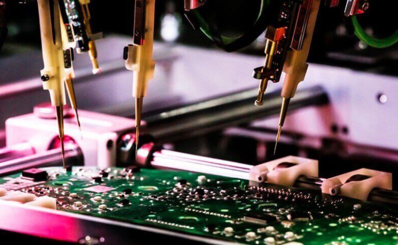
- Utilize universal testing machines (e.g., Instron 3369) equipped with 90-degree peel fixtures and operate at 50mm/min constant speed. Maintain test environment at 23±2°C and 50±5% RH to mitigate elastic modulus variations (0.7% strength deviation per °C change). Calibrate equipment quarterly and replace 304 stainless steel fixtures every three months to ensure accuracy.
3. Test Execution and Data Acquisition
- Secure specimens and initiate 90-degree peel at 50mm/min velocity. Record force-displacement curves and exclude initial peaks when calculating averages from stable-phase readings (minimum three repetitions). For a 3mm-wide sample with 3.0N average force, peel strength equals 1.0 N/mm.
4. Failure Analysis and Optimization
- Inspect interfaces for delamination (Type I: process parameter issues like inadequate 126°C lamination) or resin residue (Type II: chemical treatment anomalies). Address data dispersion exceeding 8% through equipment recalibration and sensor zeroing frequency checks. Case studies show parameter optimization reduced standard deviation from ±0.2 N/mm to ±0.05 N/mm.
5. Industry Validation Cases
- New energy vehicle PCBs employ cobalt/nickel alloy electrolytic copper foil for ≥1.2 N/mm high-temperature strength. Flexible PCBs for foldable smartphones combine PI substrates with epoxy adhesives to withstand 100,000 flex cycles without delamination. Satellite payload boards using interface-modified materials exhibit only 15% strength degradation after -55°C to 125°C cycling, outperforming conventional substrates (40% degradation).

How to Calculate Peel Strength of PCB?
1. Define Test Standards and Requirements
- International Standard Reference: Adhere to IPC-TM-650 2.4.8 (90° Peel Test), GB/T 4722-2017, or MIL-STD-275E. For instance, IPC-6012 mandates minimum peel strength of 1.0 N/mm (approximately 5.71 lb/in) at room temperature and 0.7 N/mm after high-temperature treatment (e.g., 288°C solder float for 10 seconds).
- Sample Specifications: Typical sample width is 3mm, length ≥75mm. Etch to create copper foil strips, ensuring edges are free from burrs or notches.
2. Prepare Testing Equipment and Environment
- Equipment Selection: Utilize a universal testing machine (e.g., Instron 3369) equipped with a 90-degree peel fixture for precise angle control.
- Environmental Control: Conduct tests in a constant temperature and humidity chamber (23±2°C, 50±5% RH) to minimize elastic modulus variations caused by temperature/humidity fluctuations (each °C change may induce 0.7% strength deviation).
3. Conduct Peel Test
- Secure the sample in the testing machine. Initiate 90-degree peel at 50mm/min constant velocity.
- Record real-time peel force curves. Exclude initial peak values and calculate the average of stable-phase readings (repeat ≥3 times for mean value).
- Log maximum, minimum, and average peel forces. Plot force-displacement curves to assess bonding uniformity.
4. Calculate Peel Strength
- Formula: Peel Strength (N/mm) = Peel Force (N) / Sample Width (mm).
- Example: For a 3mm wide sample with average peel force of 3.0N, peel strength = 3.0N / 3mm = 1.0 N/mm.
- Unit Conversion: 1.00 N/mm ≈ 5.71 lb/in. Select units based on client specifications.
5. Analyze and Validate Results
- Standard Comparison: Compare results against requirements (e.g., IPC-6012 room temperature ≥1.0 N/mm; military-grade PCBs may require ≥1.5 N/mm).
- Failure Mode Analysis: Inspect for delamination, fractures, or resin residue at copper-substrate interfaces to determine bonding quality. Classify failures (e.g., Type I indicates process parameter issues; Type II reflects chemical treatment problems).
- Data Dispersion Control: If intra-batch sample variation exceeds 8%, recalibrate equipment and inspect fixture status (replace 304 stainless steel fixtures every 3 months as recommended).
Welcome to contact us if you have any other issues about PCB peel strength: sales@bestpcbs.com.


