

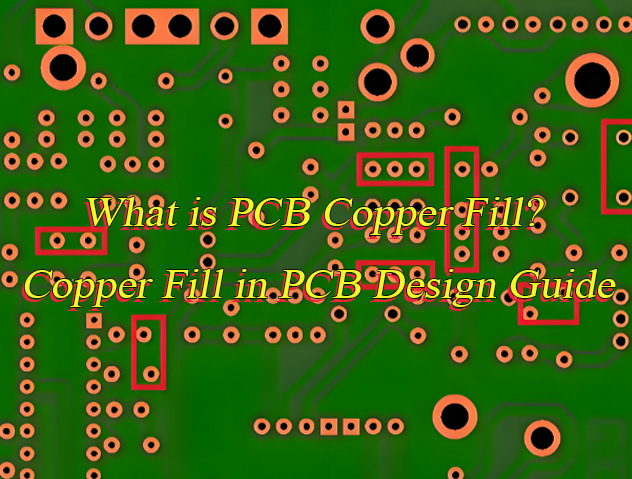
What is PCB copper fill? Let’s explore its meaning, benefits, functions, types, applications, design spec and guideline through this blog together.
Are you troubled with these problems?
- Are power components overheating and failing prematurely due to insufficient copper heat dissipation?
- Is high-speed signal crosstalk causing ghosting effects and skyrocketing EMC compliance costs?
- Are PCB warping, via fractures, and low production yields delaying your delivery schedules?
EBest Circuit (Best Technology) can provide services and solutions:
- Thermal Simulation-Driven Heat Dissipation: Real-world testing shows 20°C+ hotspot reduction, extending power component life by 50% and eliminating thermal shutdowns.
- Mesh Copper + Shielded Via Arrays: 6dB reduction in high-frequency noise, enabling first-pass FCC/CE certification and cutting 30% of compliance costs.
- Copper Balance Algorithm Optimization: Auto-adjusts copper distribution to boost SMT yield to 98%, slashes 40% production cycle time, and accelerates delivery without compromise.
Welcome to contact us if you have any request for PCB copper fill design: sales@bestpcbs.com.
What is PCB Copper Fill?
PCB Copper Fill( also called as PCB copper pour) refers to an electroplating technique that fills vias with solid copper pillars. This method addresses thermal issues in high-frequency chips and power devices, boosts current-carrying capacity (e.g., 0.3mm vias support 20A), and strengthens multi-layer board structures to prevent via wall cracking. Replacing traditional resin plugging, it uses copper’s high thermal conductivity to transfer heat rapidly to thermal layers, making it indispensable for high-current/thermal-demanding applications like 5G base stations and new energy vehicle power control modules.
What Are Advantages of PCB Copper Fill?
Benefits of PCB copper fill:
- Thermal Performance Improvment: Thermal conductivity reaches 380 W/(m·K) (vs. 0.2 W/(m·K) for resin), thermal resistance as low as 0.5 K/W. Huawei base station module tests show chip junction temperature reduction of 18℃, enabling >100W/cm² power density designs for IGBT/AI chips.
- Current-Carrying Revolution: 0.3mm via supports 20A continuous current (IPC-2152 validated), 300% higher than traditional vias. Replaces copper bars/jumpers, saving layout space and $1.2/board in BOM costs (e.g., EV motor controllers).
- Signal Integrity Enhancement: Low-impedance grounding (<0.5mΩ) reduces 5G mmWave ground bounce noise by 40%. Copper pillar shielding cuts 28Gbps high-speed signal crosstalk by 3-5dB (Cisco switch tests).
- Mechanical Strength Upgrade: 5x vibration resistance improvement, passes 20G automotive shock tests (Tesla power control modules). CTE matching extends thermal cycling life 3x (-55℃~150℃).
- High-Density Design Freedom: 0.2mm micro vias enable under-component routing, saving 40% area (Apple M-series chip packaging). Supports Any-layer HDI, reducing costs by 25% vs. laser blind vias.
What Are Functions of PCB Copper Pour?
Functions of PCB Copper fill:
- Low-Impedance Current Path Construction: Provides ultra-low-resistance channels for power (e.g., VCC) and ground (GND) networks, reducing IR drop and enabling high-current transmission (>10A/mm²) while enhancing Power Integrity (PI).
- Electromagnetic Interference (EMI) Suppression: Forms a continuous copper shielding layer to absorb high-frequency noise (>30dB@1GHz), control radiated emissions (RE), and ensure compliance with FCC/CE standards.
- Enhanced Thermal Management: Expands equivalent heat-dissipation area, boosting thermal conductivity by >15× (copper thermal conductivity: 398W/mK). It directs heat away from power devices, lowering hotspot temperatures by >20°C.
- Signal Integrity (SI) Assurance: Delivers the shortest return path for high-speed signals (≥5Gbps), mitigating ground bounce and crosstalk while maintaining impedance continuity (ΔZ < ±10%).
- Mechanical Stress Balancing: Uniformly distributes interlayer copper foil (single-layer coverage >30%) to suppress PCB warpage (<0.7% per IPC standards) and improve reflow soldering yield in multilayer boards.
- Design for Manufacturability (DFM) Optimization: Maintains copper balance (copper difference between adjacent layers <30%) to minimize etching defects and avoid over/under-etching. Reference
- Plane Segmentation: Enables precise pour boundary control to isolate digital/analog grounds, high/low voltage zones (clearance ≥2mm), and prevent noise coupling.
- Cost & Lifecycle Efficiency: Reduces risk of fine-trace breakage, cuts etching chemical consumption by >15%, and extends PCB operational lifespan.
What Are Types of PCB Copper Fill?
Common types of PCB copper fill:
1. Solid Fill
Definition: Continuous copper layer with no gaps, forming a complete conductive plane.
Features:
- Ultra-low impedance path for power/ground networks (e.g., 1oz copper supports 8A/mm² current capacity), reducing IR drop.
- 35dB shielding effectiveness for >1GHz noise, suitable for RF module protection.
- 95% pure copper thermal efficiency, lowering power device temperature rise by 15-25°C.
Design Rules:
- Slots (width ≥0.3mm) required for >100MHz to suppress eddy current loss.
- Cross-shaped thermal pads (arm width ≥0.2mm) for component pads to prevent cold solder joints.
Application Switch-mode power supply loops, automotive ECU ground planes, 5G base station RF front-ends.
2. Hatched Fill
Definition: Grid-patterned copper layer with adjustable trace width/gap (common 8-20mil), forming a perforated structure.
Features:
- 40% lower mechanical stress vs. solid fill, compatible with ceramic capacitors/BGA CTE matching.
- Grid holes suppress >100MHz eddy currents, reducing high-frequency Q-loss.
- 30% less copper usage, ideal for cost-sensitive consumer electronics.
Design Rules:
- Flex PCBs: 1:2 width/gap ratio (e.g., 10mil/20mil).
- BGA areas: 45° diagonal grid for enhanced shear strength.
- Avoid in >5A paths (50% current capacity reduction).
Application: Smartphone motherboards , wearable device flex PCBs, industrial sensor antenna zones.
3. Partitioned Fill
Definition: Independent copper zones segmented by circuit function, isolating network domains (e.g., digital/analog ground, HV/LV areas).
Features:
- Noise isolation via ≥0.5mm gap (≥2mm for 4-layer boards) between digital/analog grounds.
- 8mm clearance between 220V AC and LV domains per IEC60950 creepage standards.
- Supports multi-power domain management (e.g., Li-ion IC charge/discharge isolation).
Design Rules:
- Cross-partition traces: 100nF gap capacitors to suppress 100MHz noise.
- Smooth arc/straight-line boundaries to avoid electric field concentration.
- 1mm thermal slots in high-temperature zones (e.g., DC-DC to temperature-sensitive sensors).
Application: Medical hybrid signal boards (ECG+MCU), PV inverter HV/LV interface boards, multi-channel motor drivers.
4. Plane Layer Fill
Definition: Full-layer copper in internal PCB layers (non-surface) as signal/power reference planes.
Features:
- Stable impedance control (±7% variation) for high-speed signals (e.g., PCIe/USB4).
- Plane resistance <1mΩ (2oz copper + dense via array) for ultra-low impedance power delivery.
- Replaces 90% of power traces, improving routing channel utilization.
Design Rules:
- High-speed signal layers: ≤0.2mm spacing to reference planes for controlled impedance.
- Power plane segmentation: 3x trace width transition zone to avoid impedance discontinuity.
- Ground vias every 5mm along plane edges to suppress edge radiation.
Application: Server motherboard core power layers (12V/80A), 40Gbps optical module boards, AI accelerator cards.
When to Use Copper Fill in PCB Design?
Applications of PCB copper fill:
- High-Speed Digital Signal Integrity: Copper fill creates low-impedance reference planes (e.g., ground planes) in PCIe/DDR interfaces, reducing loop area to minimize EMI/crosstalk. For PCIe 5.0, 1oz copper with 5mil trace width achieves 85Ω±5% differential impedance.
- Low-Impedance Power Distribution: For high-power chips (FPGAs/processors), copper fill forms low-impedance power planes, reducing noise/ground bounce. Example: 3oz copper power layer with 2mil dielectric spacing for Xilinx UltraScale+ FPGA 0.85V/15A supply achieves < target impedance and 3mV ripple.
- High-Frequency EMC/Shielding: Copper fill in RF/antenna areas creates Faraday cage effects, suppressing radiation/external interference. In 5G transceivers, copper fill + shielding vias improves shielding effectiveness by 12dB over 1oz copper, meeting CISPR standards.
- Thermal Management: Copper fill under MOSFETs/power modules, paired with thermal vias, conducts heat efficiently. Industrial modules use 3oz copper + 2mm pad arrays to limit temp rise to 15°C; GaN devices achieve 290W/mK thermal conductivity via copper-filled thermal vias.
- Mechanical Strength: Inner-layer copper fill balances stress in large/multi-layer PCBs (e.g., aerospace 12-layer boards with 1oz signal/4oz power layers), preventing delamination/pad lift after thermal cycling.
- Impedance Control: Copper fill around differential pairs/transmission lines controls characteristic impedance. SATA buses use copper fill spacing/dielectric adjustments to hit 50Ω, avoiding signal distortion.
- ESD/Noise Suppression: Copper fill near interfaces (USB/HDMI) provides low-impedance discharge paths + ESD diodes, enhancing static protection. Ground plane copper fill reduces digital ground bounce by stabilizing return paths.
- Process Optimization: Uniform copper distribution improves etching/plating yield, reducing over-etching. Copper fill as solder mask underlayer prevents green oil peeling, boosting DFM.
- Test/Debug Support: Copper fill reserves test points/vias for ICT/debugging. Test fixtures connect via copper traces to measure power integrity/signal quality, speeding up testing.
- Specialized Adaptive Design: Automotive ECU boards use 2oz outer-layer copper + micro-etching for adhesion. Industrial modules adopt 4-layer 3oz copper + thermal adhesive for 3kW heat dissipation. Mobile boards leverage HDI + laser vias to balance density/copper fill.
PCB Copper Fill Design Specifications
| Parameter | Specification |
| Minimum Copper Thickness | Power Layer: ≥2oz (70μm); Signal Layer: ≥1oz (35μm) |
| Current Carrying Capacity | 1oz Copper: 8A/mm²; 2oz Copper: 15A/mm² |
| Digital-Analog Separation Gap | Digital/Analog Ground Isolation: ≥0.5mm; Power Domain Isolation: ≥2× Dielectric Thickness |
| Thermal Pad Connection Width | Conventional IC: ≥0.2mm; Power Devices: ≥0.5mm |
| Thermal Via Density | ≥4 vias/cm² (Power Area); Via Diameter ≥0.3mm |
| Ground Via Spacing | ≤λ/10 (λ=Maximum Noise Wavelength); Example: 1GHz → ≤30mm |
| Shielding Slot Width | ≥3× Skin Depth; 1GHz ≥0.2mm |
| Copper Balance Ratio (Adjacent Layers) | Copper Area Difference ≤30% |
| Mesh Fill Density | Flex PCB: 20%-40%; Rigid PCB: 40%-70% |
| Minimum Isolated Copper Size | Auto-Remove <0.25mm² Islands |
| Copper-to-Soldermask Clearance | ≥0.1mm |
| Reference Plane Integrity | No Slots Under High-Speed Signals; Split Length ≤1.5mm |
| Decoupling Capacitor Spacing | ≤λ/20 (λ=Maximum Signal Frequency); Example: 5GHz → ≤3mm |
Copper Fill in PCB Design Guide
1. Requirement Analysis
- Thermal Dissipation Requirements: Mark positions of power components and their thermal dissipation values (e.g., DC-DC converters ≥5W/cm²), requiring copper thickness ≥2oz (70μm) and thermal via arrays for optimized heat flow.
- EMI Suppression: Identify high-frequency noise sources (e.g., clock circuit harmonics), prioritizing mesh copper or continuous reference layers for shielding effectiveness.
- Structural Reinforcement: Define mechanical stress concentration zones (e.g., mounting hole perimeters), ensuring copper coverage ≥30% per board house specifications.
2. Fill Type Selection
- Solid Copper Fill: Suitable for High-current paths (e.g., power planes), critical thermal zones.
- Mesh Copper Fill: Suitable for EMC shielding, flex PCB anti-bending designs.
- Cross-Hatch Copper: Suitable for High-speed signal reference layers (e.g., beneath differential pairs).
- Hybrid Fill Strategies: Suitable for Combine solid copper (near power devices) and mesh copper (peripheral shielding) in mixed-requirement zones.
3. Safety Clearance Standards
- High-Voltage Zones (e.g., AC/DC isolation): Creepage distance ≥2mm per IPC-2221, considering pollution degree and material CTI (Comparative Tracking Index).
- Signal Trace Proximity: Maintain 3× trace width spacing to avoid parasitic capacitance effects (critical for high-speed digital signals requiring impedance matching).
- Board Edge Clearance: ≥5mm copper-free zone to prevent delamination during V-CUT scoring; CNC machining zones require ≥0.5mm buffer.
4. Net Connection Strategies & Thermal Management
- Power Device Connections: Full connectivity + thermal via arrays: Via diameter 0.3mm, pitch ≤1.5mm (quantity calculated via thermal resistance formulas), enhanced by thermal interface materials (e.g., Bergquist SIL-PAD).
- Sensitive Signal Areas: Cross-connections (4mil width) or “star” topologies to minimize thermal stress coupling into analog front-ends (e.g., ADC circuits).
5. Via System Design & Reliability
- Thermal Vias: Densely placed beneath heat-generating components, with via dimensions and counts validated via thermal simulation (e.g., ANSYS Icepak) to ensure hotspot temperatures ≤85°C for industrial-grade components.
- Shielding Vias: Placed around high-frequency noise sources, with spacing ≤λ/10 of the noise wavelength (e.g., ≤30mm for 100MHz noise), forming Faraday cages with ground planes.
- Prohibited Zones: No vias within 3mm of BGA packages to prevent solder joint fatigue; utilize blind/buried vias for optimized interlayer connectivity.
6. Simulation Verification and Multi-Physics Analysis
Thermal-Electric-Mechanical Coupling:
- Thermal Simulation: Validate hotspot temperatures and thermal gradients using tools like ANSYS Icepak, optimizing copper thickness and via layouts.
- Current Density Verification: Ensure ≥30% margin in current-carrying capacity via SI9000 to prevent electromigration failures.
- Signal Integrity Analysis: Check impedance matching, crosstalk, and ground bounce using SI/PI tools, with emphasis on reference layer continuity for high-speed designs.
DFM Checks: Align copper fill with solder mask registration errors ≤0.1mm, verifying manufacturability (etch uniformity, layer alignment accuracy).
7. Production File Output and Process Control
Gerber Specifications:
- Dedicated copper fill layers labeled (e.g., GND/PWR planes), distinguishing signal and power layers.
- Drill files differentiate PTH (plated through-holes) and NPTH (non-plated), with tolerance annotations (e.g., ±0.1mm).
Process Notes:
- Copper thickness tolerances (e.g., outer layers ±10% for 2oz), solder mask opening dimensions, and surface finishes (e.g., ENIG, HASL).
- Stack-up documentation: Core thickness, dielectric materials (FR4/high-speed substrates), dielectric constant, and loss tangent values.
8. Design Prohibitions
- RF Circuits: Random copper fill prohibited above 1GHz; use continuous reference layers to minimize signal loss.
- Analog Small-Signal Areas: Maintain ≥0.5mm copper-free isolation to avoid digital noise coupling.
- Mechanical Reliability: Copper fill edges ≥0.5mm from board profile to prevent CNC-induced copper lifting; reinforce mounting hole perimeters with annular fills.
- Design for Test (DFT): Reserve test points (e.g., Via-in-Pad) in copper-filled zones for ICT accessibility and fault diagnostics.
FAQs of Copper Fill in PCB Design
Q1: How should different ground lines (like digital ground) be properly connected in PCB design to avoid interference?
A1: Use single-point connection methods via 0Ω resistors, ferrite beads, or inductors. For example, separate digital and analog ground planes with independent copper pours, each referenced to the primary “ground” as a benchmark. This prevents ground loop currents and interference. Additionally, widen power traces (e.g., 5.0V, 3.3V) into polygonal structures to minimize impedance and voltage drop.
Q2: Why does a crystal oscillator require special copper treatment around it? How is this implemented?
A2: As a high-frequency emission source, a crystal oscillator needs a grounded copper enclosure around it to reduce high-frequency signal interference to adjacent circuits. In practice, the oscillator’s case should be separately grounded, with via holes added in the copper area to ensure electrical continuity and avoid isolated islands or antenna effects.
Q3: How to resolve “isolated copper islands” (dead zones) in PCB design?
A3: Isolated islands are copper blocks disconnected from the main copper area. Solutions include adding ground vias to connect to the primary ground plane or assigning the region to a specific ground network. Small islands can be deleted, while larger ones require grounding via vias to prevent noise generation or manufacturing defects.
Q4: What are the pros and cons of mesh copper vs. solid copper in PCB design?
A4: Solid copper offers strong conductivity and thermal dissipation but may cause board warping or blistering. Mesh copper provides uniform heat distribution and excellent EMI shielding but has lower current-carrying capacity. High-frequency circuits benefit from mesh copper to reduce interference, while high-current or low-frequency designs favor solid copper. Note that overly small mesh sizes may lead to manufacturing issues like etching unevenness.
Q5: How does copper thickness impact signal integrity and current-carrying capacity in PCBs?
A5: Copper thickness directly affects impedance control and current capacity. Thick copper (e.g., 2oz) reduces trace resistance, minimizing signal attenuation and crosstalk, making it ideal for high-speed signals or high-current applications. Thinner copper supports finer routing but may require tighter line width/spacing control (e.g., ~6-8mil for 2oz copper) to avoid manufacturing limitations like side etching.