

How to choose PCB cloning service supplier? Let’s discover benefits, application, clone process, selection guide, cost and delivery time for PCB cloning service.
Are you troubled with these problems?
- Design files lost, version chaos, how to rapidly restore discontinued PCB prototypes?
- Original technical support discontinued, how to cost-effectively replicate legacy circuit boards without spare parts?
- Reverse engineering time-consuming and material-wasting, how to shorten cloning cycles to seize market opportunities?
As a PCB cloning service supplier, EBest Circuit (Best Technology) can provide you service and supplier:
- Intelligent Deconstruction + Data Reconstruction– No original data required. Achieve 1:1 circuit topology replication via physical-layer reverse engineering, delivering verifiable Gerber files within 72 hours.
- Material-Level Adaptation – Address component substitution needs with matched impedance/capacitance values and package-compatible BOM optimization, reducing procurement costs by over 30%.
- Mass Production Validation Closed Loop – From prototype cloning to batch production, offer full-chain support including signal integrity testing and thermal simulation validation, ensuring cloned boards deliver identical functionality to originals.
Welcome to contact us if you have any request for PCB cloning service: sales@bestpcbs.com.
What Is PCB Cloning Service?
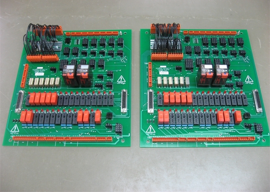
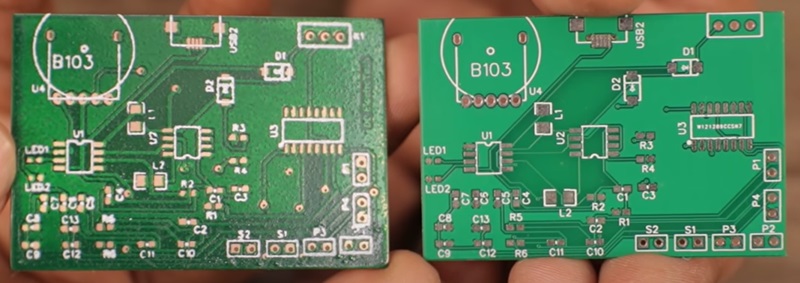
PCB cloning service, also commonly known as PCB copying, circuit board reverse engineering, PCB reverse engineering or PCB replication, refers to the analysis and measurement of existing physical printed circuit boards through technical means to obtain their complete physical structure, wiring information, components list (BOM) and layout details. The ultimate goal is to be able to completely replicate (clone) a functionally identical circuit board or obtain its design files.
Why Choose PCB Cloning Service?
Advantages of PCB Cloning Service:
- Accelerate Market Entry: Achieve 1:1 precise replication and secondary development to launch new products within weeks, avoiding market share loss caused by lengthy R&D cycles.
- Slash Development Costs by 30%-50%: Bypass high R&D expenses by leveraging existing mature designs for functional optimization, significantly boosting profit margins.
- Democratize Premium Technology: Localize high-end imported products to reduce prices to 1/3-1/2 of original costs, rapidly expanding market reach and customer base.
- Ensure Reliable Performance: Use high-temperature-resistant and vibration-proof materials for stable operation in -40°C to 125°C environments, reducing failure rates by 40% and extending product lifespan.
- Boost Production Efficiency by 50%: Standardized designs enable automated manufacturing, shortening lead times to 7-15 days and meeting urgent delivery demands.
- Drive Industry Innovation Cycles: Reverse engineering fuels forward R&D advancements, positioning companies to lead in technology upgrades and maintain competitive edge.
When to Use PCB Cloning Services?
Applications of PCB Cloning Services:
- Aging Equipment Maintenance and Spare Part Replacement: When equipment fails due to PCB damage and the original manufacturer no longer provides spare parts or services, cloning services can replicate the original PCB to rapidly restore equipment operation. For instance, in medical devices, cloning an outdated control board avoids costly replacement expenses.
- Rapid Prototype Verification and Functional Testing: During new product development, cloning existing PCBs enables quick validation of design feasibility. Consumer electronics companies, for example, clone existing motherboards to test new functional modules, reducing development cycles.
- Reverse Engineering and Patent Avoidance: To analyze competitor product designs or circumvent patent restrictions, cloning services decode PCB structures to extract design details. Industrial control equipment manufacturers, for example, analyze competitive PCB layouts to optimize their own designs.
- Production Recovery and Supply Chain Security: When original manufacturers cease production or supply chains are disrupted, cloning replicates PCB designs to ensure production continuity. Automotive electronics suppliers, for instance, clone critical PCBs to maintain production line operations when original manufacturers discontinue services.
- Compatibility Upgrades and Customization Needs: When upgrading existing equipment functionality while maintaining compatibility, cloning modifies original designs while preserving interfaces. Industrial automation equipment, for example, clones original PCBs and adds new interfaces when upgrading communication modules to ensure compatibility with legacy systems.
- Educational and Research Applications: Educational institutions or research organizations clone classic PCB designs for teaching or experimentation. Electronic engineering courses, for example, clone classic microcontroller boards for student practice and learning.
- Legal and Intellectual Property Compliance: Within legal boundaries, cloning verifies product compliance with patent requirements or facilitates design improvements. Enterprises, for example, analyze competitive PCBs through cloning to ensure their designs do not infringe on intellectual property rights.
How to Clone a PCB Board?
A Comprehensive Guide to Cloning PCB Boards:
Step 1: Precise Data Collection and Component Analysis
- High-Precision Image Acquisition: Utilize industrial-grade scanners (resolution ≥1200 DPI) to capture high-definition images of both sides of the PCB, ensuring no details of copper traces, pads, or silk-screen layers are missed.
- Comprehensive Component Parameter Documentation: Take high-resolution photos of component layouts, documenting each component’s model (e.g., SMD resistor 0805 package), parameters (e.g., capacitor 10μF/25V), polarity (e.g., electrolytic capacitor anode/cathode markers), and IC orientation (e.g., DIP package pin 1 position).
- Pad Cleaning and Preparation: After disassembling components, use specialized PCB cleaning solutions or ultrasonic cleaners to remove solder residue, ensuring copper layers are oxidation-free and clean for subsequent scanning.
Step 2: Image Preprocessing and Layer Separation
- Image Enhancement and Binarization: Adjust image contrast/brightness via Photoshop or professional PCB software, converting color scans to black-and-white binary images to ensure clear distinction between copper traces and substrate (tolerance ≤0.05mm).
- Multilayer Board Layer Separation: For multilayer boards, polish each layer until copper surfaces shine, then scan; align layers using fiducial marks/holes with professional tools (e.g., CAM350) to ensure precise via-pad alignment.
- Defect Detection and Correction: Use software to automatically detect shorts/opens, followed by manual verification to fix image artifacts (e.g., scratches, stains causing misinterpretation).
Step 3: PCB Layout Reconstruction and Library Creation
- EDA Software Integration: Import processed images into Altium Designer/OrCAD, layering traces, pads, vias, and silk-screen layers while defining parameters like trace width/spacing (e.g., 6mil/6mil) and copper thickness (e.g., 1oz).
- Component Library Development: Catalog all component packages (e.g., SOP, QFP, BGA), create standardized footprints matching physical components, and generate BOM lists aligned with actual parts; if original components are obsolete, select compatible alternatives after electrical verification.
- 3D Model Validation: Use software 3D previews to check component placement for mechanical clearance or thermal issues, ensuring no interference.
Step 4: Schematic Reverse Engineering and Logic Verification
- Schematic Extraction and Simulation: Derive schematics from the reconstructed PCB layout, validate circuit logic using Multisim/LTspice, correct shorts/opens, and ensure signal integrity (e.g., impedance matching, signal delay).
- Multilayer Signal Integrity Analysis: For multilayer boards, assess cross-layer signal coupling, power/ground plane integrity, and optimize routing to minimize noise (e.g., adding decoupling capacitors, ferrite beads).
- Functional Simulation Testing: Simulate real-world operating conditions to verify circuit functionality, ensuring cloned boards match original electrical performance.
Step 5: Production File Generation and Process Optimization
- Gerber File Export: Generate IPC-compliant Gerber files specifying copper thickness, hole sizes, solder mask parameters, etc., for precise PCB manufacturing.
- BOM Optimization and Sourcing: Compile component lists, prioritizing mainstream suppliers (e.g., TI, ST) for supply chain stability; if cost reduction is needed, verify electrical compatibility of alternative parts.
- Process Parameter Definition: Specify manufacturing requirements like minimum trace/spacing, surface finishes (HASL/ENIG), solder mask colors, and DFM (Design for Manufacturability) compliance.
Step 6: Prototype Fabrication and Assembly Validation
- Prototype Production and Inspection: Submit Gerber files to certified PCB manufacturers for prototype production; verify layout accuracy via 1:1 laser-printed transparencies and use flying probe testing to detect connectivity issues (e.g., solder joints, shorts).
- Component Soldering and Inspection: Assemble components per BOM, employ X-ray inspection for hidden solder joints (e.g., BGAs), and validate signal integrity with oscilloscopes/logic analyzers to confirm functionality.
Step 7: Comprehensive Functional Testing and Reliability Validation
- Electrical Parameter Testing: Power up cloned boards to measure voltage, current, signal integrity, etc., comparing against originals to ensure deviations are within tolerance (e.g., ±5%).
- Environmental and Reliability Testing: Conduct accelerated aging (85°C/85% RH for 168 hours), thermal cycling (-40°C to 125°C), vibration testing (IEC 68-2-6), and EMC compliance verification (e.g., CE/FCC) to match original board stability and reliability.
- Mass Production Readiness: After passing all tests, compile complete production documentation (Gerber, BOM, process files) and initiate mass production, ensuring consistent quality from prototype to batch.

How to Choose a PCB Cloning Service Supplier?
Below Are PCB Cloning Service Supplier Selection Guides:
1. Technical Capability Deep Verification
- High-Precision Equipment Configuration: Prioritize suppliers equipped with industrial-grade high-precision scanners (resolution ≥1200DPI), professional PCB design software (e.g., Altium Designer, CAM350), and 3D simulation tools (e.g., ANSYS), ensuring data acquisition precision reaches the micrometer level (error ≤5μm) and supporting precise reconstruction with interlayer alignment error ≤0.05mm for multilayer boards.
- Engineer Experience Validation: Require the engineering team to have over 5 years of experience in PCB cloning projects, particularly in complex multilayer boards (e.g., 12+ layers), high-density interconnect (HDI) boards, and high-frequency/high-speed boards, with technical whitepapers or patents to demonstrate innovation capabilities.
2. Full-Cycle Quality Control Coverage
- Multidimensional Testing Standards: Confirm the supplier employs full-cycle quality inspection methods including flying probe testing (precision ±1μm), X-ray inspection (for BGA package penetration), AOI optical inspection (solder joint defect rate ≤0.1%), and accelerated aging tests (85°C/85% RH for 168 hours + 1000 thermal cycles) to ensure electrical performance, mechanical strength, and environmental adaptability meet standards.
- International Standard Compliance: Verify adherence to IPC-A-610 Class 2/3, ISO 9001 quality management systems, and RoHS environmental standards, with third-party certification reports (e.g., UL) to ensure traceable production processes and controlled quality.
3. Compliance and Legal Risk Mitigation
- Reverse Engineering Legitimacy: Ensure the supplier only accepts legally authorized reverse engineering requests (e.g., repairing discontinued components, replacing obsolete parts) and signs legally binding NDAs (Non-Disclosure Agreements) specifying technical secret protection scope, breach liability, and dispute resolution mechanisms.
- Intellectual Property Compliance: Confirm the supplier has established an IP review mechanism to avoid infringing third-party patents or trademarks during cloning, with compliance statements and legal opinions to minimize legal dispute risks.
4. Full-Process Technical Support and Responsiveness
- End-to-End Technical Support: Assess whether the supplier provides full-process technical support from data acquisition, layout reconstruction, schematic validation to mass production, including real-time progress updates (e.g., daily reports), rapid issue resolution (24-hour response), and customized design optimization (e.g., signal integrity enhancement, EMC/EMI suppression).
- Delivery Cycle Flexibility: Confirm negotiable delivery timelines with support for rush orders (e.g., 72-hour rapid prototyping) and a production tracking system for real-time status monitoring.
5. Cost Transparency and Cost-Effectiveness Optimization
- Detailed Quotation Breakdown: Require transparent quotes detailing scanning, design, testing, material, and labor costs per phase, avoiding hidden fees (e.g., template fees, rework charges), with cost comparison reports to help select the most cost-effective solution.
- Cost-Effectiveness Evaluation Model: Establish a multidimensional evaluation model considering technical metrics (precision, reliability), service responsiveness, compliance safeguards, and long-term partnership potential, prioritizing suppliers with the lowest unit cost under equivalent technical standards and controlled risks.
6. Customer Feedback and Case Validation
- Third-Party Review Verification: Obtain customer reviews via authoritative platforms (e.g., Trustpilot, Google Reviews) or independent third-party agencies, focusing on supplier performance in complex projects (e.g., high-layer cloning, high-frequency optimization), and verify review authenticity by contacting past clients.
- In-Depth Case Study Analysis: Require detailed case reports from suppliers, including project background, technical challenges, solutions, and outcomes, particularly innovative approaches (e.g., AI-assisted routing optimization, thermal management improvements) in high-complexity projects to validate problem-solving capabilities.
7. Customized Design and Full-Link Support
- Design Optimization Capability: Confirm support for customized design optimization based on product iteration needs, such as signal integrity enhancement (via impedance matching, decoupling capacitors), thermal management improvements (adding thermal pads, thermal materials), and DFM (Design for Manufacturability) optimization to reduce production defects, with design validation reports and simulation data.
- Full-Link Production Support: Evaluate whether the supplier offers end-to-end support from prototyping to mass production, including production file generation (Gerber, BOM), process parameter setting (surface finishes, solder mask colors), and supply chain management (component sourcing, logistics coordination), ensuring seamless transition of design optimizations to mass production and full-process control.
How Long Does PCB Cloning Service Take?
| PCB Type | Design Files Only | Design + Bare PCB | Full Assembly (PCBA) |
| 1-2 Layer Simple | 2-3 days | 4-6 days | 6-8 days |
| 4 Layer Standard | 3-5 days | 6-9 days | 8-12 days |
| 6-8 Layer Complex | 7-12 days | 12-18 days | 15-25 days |
| HDI/Advanced | Quote upon review | +30-50% lead time | +40-60% lead time |
How Much Does PCB Cloning Service Cost?
| Complexity Level | Typical Application Scenarios | Cloning Service Quote | Total Prototyping Cost (10 units) |
| Simple Board | Single/Double-sided board, <50 components | $150–$500 | $300–$800 |
| Medium Board | 4-6 layer board, with BGA/standard ICs | $800–$3,000 | $2,000–$6,000 |
| Advanced Board | 8+ layer with HDI/blind/buried vias, for AI server boards | $5,000–$20,000+ | $15,000–$50,000+ |
FAQs of PCB Cloning Service
Q1: Will the cloned PCB match the original board’s performance? How is it scientifically verified?
A1: Performance consistency is ensured through high-precision scanning (error ≤5μm), signal integrity simulation (impedance matching, EMC/EMI noise suppression), and full-cycle testing including 85°C/85% RH 168-hour aging tests and IEC 68-2-6 vibration tests. Suppliers provide third-party certified test reports (e.g., IPC-A-610 Class 3) and real-time data comparisons, supporting on-site or third-party lab verification for quantifiable performance matching.
Q2: How is my design data and intellectual property secured during cloning?
A2: Legitimate suppliers execute legally binding NDAs to define IP protection scope (schematics, process parameters), liability, and dispute resolution. Data security measures include bank-grade encryption, multi-tier access controls, and audit trails. Cloning is restricted to authorized reverse engineering (e.g., replacing discontinued components) to prevent leaks or misuse, complying with global IP standards.
Q3: Can cloning services optimize performance for product evolution needs?
A3: Yes, customization includes signal integrity enhancements (reduced signal delay via impedance optimization), thermal improvements (thermal pads/materials for heat dissipation), and DFM (Design for Manufacturability) optimizations to minimize defects. Suppliers provide quantified simulation data (thermal/EM field analysis) and validation reports to ensure traceable, verifiable performance upgrades.
Q4: Are cloning costs fully transparent? Are there hidden charges?
A4: Total costs cover scanning, design, testing, materials, and labor with transparent pricing. Suppliers provide detailed quotes breaking down each phase (e.g., scanning, design, testing) and comparative analyses (vs. OEM/other vendors) to eliminate hidden fees, ensuring budget predictability.
Q5: Do cloned PCBs meet international quality standards? How is quality controlled?
A5: Cloned boards adhere to IPC-A-610, ISO 9001, RoHS, and other global standards. Suppliers provide third-party certifications (e.g., UL) and full-traceability quality records (flying probe tests, X-ray inspection for hidden joints, AOI defect rates ≤0.1%). Multi-dimensional testing (aging for reliability, vibration for mechanical integrity) ensures process traceability and consistent quality for global clients.