

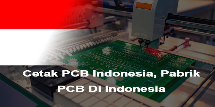
Looking for cetak PCB Indonesia service? This blog is mainly about pain points and solutions of cetak PCB Indonesia, and how to evaluate the production capacity and lead time of pabrik PCB di Indonesia.
Amid Indonesia’s fast-growing electronics sector which is particularly driven by the expanding electric vehicle (EV) and battery manufacturing ecosystem cetak PCB Indonesia serves as a cornerstone for supporting local production and fostering innovation. Securing a reliable partner for cetak PCB Indonesia is essential to safeguarding product quality and keeping project timelines on track with a market landscape that includes a wide range of production entities from small-scale production units to large-scale manufacturing hubs. This guide focuses on addressing core needs tied to PCB manufacturing Indonesia, pabrik PCB di Indonesia, and PCB assembly Indonesia offering practical insights to navigate Indonesia’s PCB sector effectively and make confident decisions for your projects.
Are You Facing These Problems?
- Do you struggle with inconsistent quality in cetak PCB Indonesia, such as solder defects or uneven copper cladding that affects product performance?
- Is the long lead time for custom PCB Indonesia causing delays in your project timeline, especially for urgent prototype needs?
- Have you encountered hidden costs with pabrik PCB di Indonesia that were not disclosed in the initial quote, increasing overall project expenses?
- Do you lack professional technical support during the design phase, leading to rework and additional costs in cetak PCB Indonesia?
- Is the reliability of delivery a concern, with frequent missed deadlines from pabrik PCB di Indonesia affecting your production schedule?
End-to-End Guarantee from Requirement to Delivery
- Pre-production Technical Consultation: Free DFM analysis proactively identifying manufacturability risks upfront, reducing rework rates by up to 30% and ensuring smooth execution of your cetak PCB Indonesia projects.
- Transparent Pricing System: Itemized quotes for your PCB manufacturing Indonesia-related needs with no hidden fees, covering production, international logistics and customs clearance costs. This helps you accurately forecast budgets and avoid cost overruns common with many local or regional suppliers.
- Smart Production Scheduling: Advanced MES for real-time monitoring and dynamic scheduling, ensuring stable lead times (±1 day) for custom PCB Indonesia orders. A 15% capacity buffer handles urgent orders efficiently, with optimized international shipping routes to shorten cross-border delivery cycles.
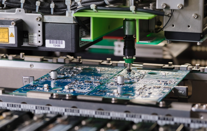
- Strict Quality Control: Three-stage inspection (IMI, IPI, FI) with AOI and flying probe testing, 8+ quality checkpoints, and defective rate below 0.05%. This ensures we deliver consistent quality that meets your cetak PCB Indonesia requirements before cross-border shipment.
- Real-Time Progress Tracking: 24/7 online portal for your PCB assembly Indonesia orders, covering the entire cross-border production and delivery process. Automatic milestone notifications (production completion, shipment, customs clearance, arrival) eliminate repeated follow-ups.
- After-Sales Support: 24-hour response for your cetak PCB Indonesia orders. For quality issues, root cause analysis and solutions like replacement are provided within 48 hours, plus a 1-year warranty for mass production. We also offer dedicated international after-sales coordination to resolve cross-border issues efficiently.
Why Choose EBest Circuit (Best Technology) for Cetak PCB Indonesia?
Reasons Why Choose EBest Circuit( Best Technology) for cetak PCB Indonesia:
- Competitive Pricing & Cost-Sensitive Solutions: Tailor cost optimization plans based on your project requirements, achieving 15%-22% cost reduction for PCB manufacturing Indonesia projects. We leverage bulk material procurement and optimized cross-border logistics to balance quality and cost, with an average of 300+ cross-border cost optimization consultations processed daily.
- 24-Hour Rapid Prototyping: Support urgent prototype orders with 24-hour turnaround time for cetak PCB Indonesia, with a daily processing capacity of 200+ urgent prototype orders. This accelerates your project iteration speed by 40% compared to industry average, and the prototype delivery on-time rate reaches 99.8%.
- High On-Time Delivery Rate: Maintain a 99.2% on-time delivery rate for cross-border shipments through efficient production management and optimized international logistics routes. For your pabrik PCB Indonesia-related orders, we ensure cross-border customs clearance efficiency is improved by 40%, and the annual delay rate for cross-border deliveries is less than 0.8%.
- Superior Quality Assurance: Implement strict quality control processes with AOI optical inspection coverage of 100% for mass production. The defective rate of bulk products is controlled below 0.05% (industry average is 0.5%), and all products comply with international standards to ensure reliable cetak PCB Indonesia products. We also pass 100% of high and low temperature stability tests (-40℃~+85℃) to meet harsh application environments.
- 19 Years of Industry Experience: With nearly two decades of experience in the PCB industry, we have served 8000+ global customers and completed 45000+ cross-border PCB projects. Our mature technologies and rich experience help customers reduce overall project costs by an average of 18%, and shorten the project cycle by 25%.
- Free DFM Analysis: Provide professional DFM analysis services free of charge, with an analysis accuracy rate of 98.5%. This optimizes design schemes for custom PCB Indonesia, reduces design rework costs by 30%, and improves production efficiency by 28%, with an average of 12 days shortened in the design verification cycle.
- Authoritative Certifications: Hold multiple international certifications including ISO9001:2015, ISO13485:2016, REACH, RoHS, and IATF16949. Our annual third-party quality audit pass rate is 100%, and all products exported to Indonesia meet local quality and environmental standards, ensuring compliance with global trade requirements.
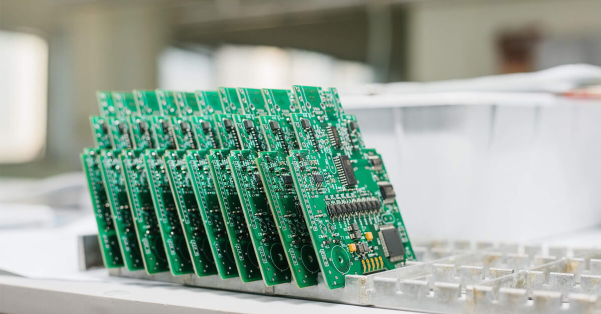
- One-Stop Service Capability: Cover the entire process from design optimization, prototyping, mass production to assembly, offering integrated PCB assembly Indonesia solutions. This simplifies your supply chain management, reduces the number of cooperative suppliers by 60%, lowers supply chain management costs by 30%, and shortens the overall project cycle by 40% with SMT placement accuracy up to ±0.03mm.
Top Pabrik PCB Di Indonesia List
| Company Name | Main Business | Core Advantages | Process Capability & Lead Time |
| Best Technology Circuit Co., Limited (EBest Circuit Co., Limited) | Cetak PCB Indonesia, custom pcb indonesia, pcb assembly Indonesia, high-precision PCB manufacturing | 19 years of experience, free DFM analysis, 24-hour rapid prototyping, multiple international certifications | Process capability: 2-32 layers PCB, minimum line width/space 3mil/3mil; Lead time: 24h for urgent prototypes, 5-7 days for mass production |
| PT. Intertech Circuit Indonesia | PCB manufacturing, SMT assembly, electronic component distribution | Local production base, quick response to local needs, competitive pricing for small and medium batches | Process capability: 2-16 layers PCB; Lead time: 7-10 days for prototypes, 10-15 days for mass production |
| PT. Electronic Circuit Indonesia | Double-sided and multi-layer PCB manufacturing, PCB assembly services | Strict quality control system, long-term cooperation with local electronics enterprises | Process capability: 2-20 layers PCB; Lead time: 5-8 days for prototypes, 12-18 days for mass production |
| PT. Prima Circuit Nusantara | Custom PCB manufacturing, high-frequency PCB production, PCB testing services | Specialized in high-precision products, professional testing equipment, technical support team | Process capability: 2-24 layers PCB, high-frequency material processing; Lead time: 8-12 days for prototypes, 15-20 days for mass production |
Types of Cetak PCB Indonesia Services
- Prototype PCB Printing: Rapid prototyping for small-batch trial production, supporting quick design verification for custom PCB Indonesia.
- Mass Production of Double-Sided PCB: Cost-effective manufacturing solutions for standard double-sided PCB products, suitable for various electronic devices.
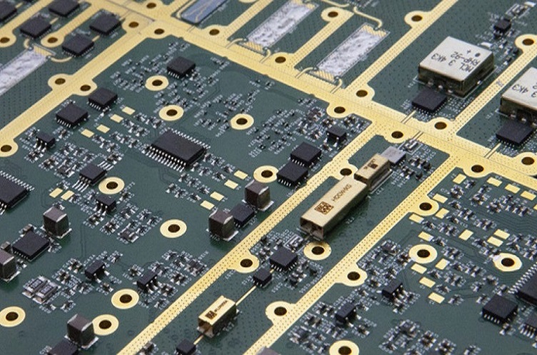
- Multi-Layer PCB Manufacturing: Production of 4-32 layers high-precision multi-layer PCBs, meeting the needs of complex electronic products.
- High-Frequency PCB Printing: Specialized manufacturing for high-frequency PCBs using advanced materials, suitable for communication and radar equipment.
- Flexible PCB Production: Flexible and rigid-flex PCB manufacturing, adapting to special installation environments.
- PCB Assembly Services: One-stop assembly services including SMT, DIP, and testing, completing the transformation from PCB to finished products.
- Custom PCB Design and Manufacturing: Tailored solutions based on specific project requirements, covering design optimization and production.
- PCB Testing and Inspection Services: Including electrical performance testing, visual inspection, and reliability testing to ensure product quality.
How to Evaluate the Production Capability of Pabrik PCB Di Indonesia?
Evaluation Guide to Production Capability of Pabrik PCB Di Indonesia:
- Check Core Process Parameters: Verify minimum line width/space (reliable standard ≥4mil/4mil), minimum hole diameter (mechanical drilling ≥0.2mm) and maximum layers (mainstream factories support 2-24 layers, high-end products ≥18 layers). These parameters directly reflect process precision.
- Inspect Key Production Equipment: Focus on advanced equipment indicators, such as exposure machine alignment accuracy (≤5μm for high-precision models) and electroplating line performance (hole copper thickness ≥20μm). Equipment aged within 5 years ensures more stable process quality.
- Review Quality Control System: Confirm the number of quality inspection procedures (full-process ≥18 checks is preferred) and pass rate data (finished product yield ≥99.5% indicates reliable control). Prioritize factories with three-stage inspection (incoming, in-process, final).
- Verify Certifications: Check for ISO9001, IATF16949 certifications, and third-party audit pass rate (100% pass rate is a basic requirement). Certifications ensure compliance with global quality standards for cetak PCB Indonesia projects.
- Request Sample Testing: Evaluate sample indicators such as surface flatness (warpage ≤0.75mm/m), solder joint qualification rate (≥99.8%) and dimensional tolerance (±0.05mm). Samples directly reflect actual production capacity.
- Inquire About Material Sources: Confirm raw material standards, such as copper clad laminate grade (FR-4 for general use, high-frequency materials for special needs) and copper foil thickness (≥1oz for standard products). High-quality materials are the basis of reliable processes.
- Assess Technical Support: Evaluate DFM analysis capability and problem-solving response time (≤24 hours is ideal). Professional technical support reduces rework risks in custom PCB Indonesia projects.
- Review Project Cases: Check cooperation experience in similar industries and the success rate of complex projects (≥95%). Rich cases prove adaptability to specific process requirements.
How to Evaluate the Lead Time of Perusahaan PCB Di Indonesia?
Evaluation Guide to Lead Time of Perusahaan PCB Di Indonesia:
- Confirm Standard Lead Time: Clarify standard cycles by product type – prototypes (5-10 days), small batches (10-15 days), mass production (15-25 days) – to match your project timeline.
- Inquire About Urgent Order Capability: Confirm if 24-hour rapid prototyping for Cetak PCB Indonesia is available, with urgent order on-time delivery rate ≥99% as a reliable benchmark.
- Evaluate Production Scheduling System: Prioritize plants with intelligent systems that reduce delivery commitment deviation by ≥36% and cut scheduling cycle from 12h to 1.5h.
- Review On-Time Delivery Rate Data: Request historical data – reliable factories have on-time rate ≥99%, with annual delay rate ≤1% (industry average 3%).
- Understand Capacity Reserve: Inquire about production capacity and reserve (≥15% reserve capacity preferred) to meet peak-season order demands without delays.
- Check Logistics Cooperation: Confirm cooperative logistics providers offer Indonesia-focused solutions, with cross-border clearance time ≤3 days and transportation damage rate ≤0.1%.
- Clarify Delivery Delay Policies: Understand compensation terms – e.g., 3% order value compensation for 1-3 days delay, 5% for over 3 days – to mitigate project risks.
- Request Progress Tracking Mechanism: Confirm real-time tracking services with updates every 4 hours and abnormal situation response time ≤2 hours.
FAQs of PCB Manufacturing Indonesia
Q1: How to solve serious solder joint defects (e.g., cold soldering, bridging) in PCB prototypes?
A1: Optimize reflow soldering parameters, strictly control solder paste quality, and implement in-process inspection for timely rework. Provide pre-production DFM analysis for custom PCB Indonesia to optimize pad design and reduce defect risks.
Q2: What to do if mass production delivery delays affect subsequent schedules?
A2: Adopt intelligent MES scheduling system, maintain 99.2% on-time delivery rate, and reserve capacity for unexpected orders. Provide real-time progress tracking to keep you updated on production status.
Q3: How to prevent and solve PCB warpage affecting assembly accuracy?
A3: Use high-quality low-warpage copper clad laminates, optimize heat treatment process, and conduct strict flatness testing. Provide professional leveling for slight warpage and custom fixtures for high-precision projects.
Q4: How to avoid hidden costs (e.g., additional testing/material fees) in orders?
A4: Offer transparent itemized quotes covering production, logistics and customs clearance. Confirm requirements in detail before production and provide cost breakdown sheets for PCB manufacturing Indonesia projects.
Q5: How to solve design schemes unsuitable for mass production causing rework?
A5: Provide free professional DFM analysis (98.5% accuracy) to optimize design parameters. Communicate production constraints in advance for custom PCB Indonesia, reducing rework rates and costs.