

PCB assembly India has emerged as a competitive hub for global electronics manufacturing, driven by continuous technology iteration and advanced infrastructure upgrades. Businesses worldwide leverage PCB assembly India for a balanced combination of cost-effectiveness and strict compliance with international quality standards, solidifying its position as a go-to choice for both prototype development and high-volume production requirements.
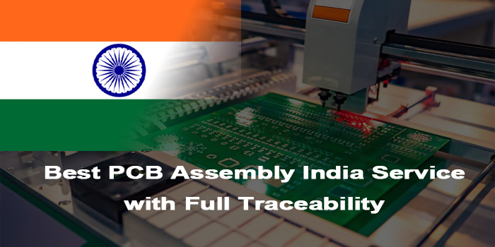
Why Choose PCB Assembly India Service?
- Government-backed incentives via “Make in India” and PLI schemes, reducing operational costs for manufacturers.
- Competitive labor and operational expenses, lowering overall project costs without compromising quality.
- Skilled workforce proficient in handling complex assembly processes and global certifications.
- Advanced infrastructure with SMT lines, AOI, and X-ray inspection tools meeting IPC-A-610 standards.
- Growing domestic demand creating a robust ecosystem for PCB manufacturing and assembly India.
- RoHS and ISO 9001 compliance, ensuring products meet global environmental and quality norms.
- Proximity to key electronics markets, enabling faster logistics and reduced shipping lead times.
- Flexible services catering to low-volume prototypes and high-volume mass production requirements.
Types of PCB Assembly Services in India
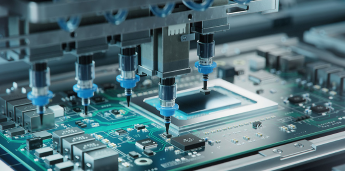
- SMT PCB assembly: The most in-demand option for compact, high-density designs, supporting fine-pitch components and high-volume production with advanced placement and reflow technology.
- Through-hole assembly: Ideal for rugged applications requiring strong mechanical stability, suitable for components that need to withstand vibration or high-temperature environments.
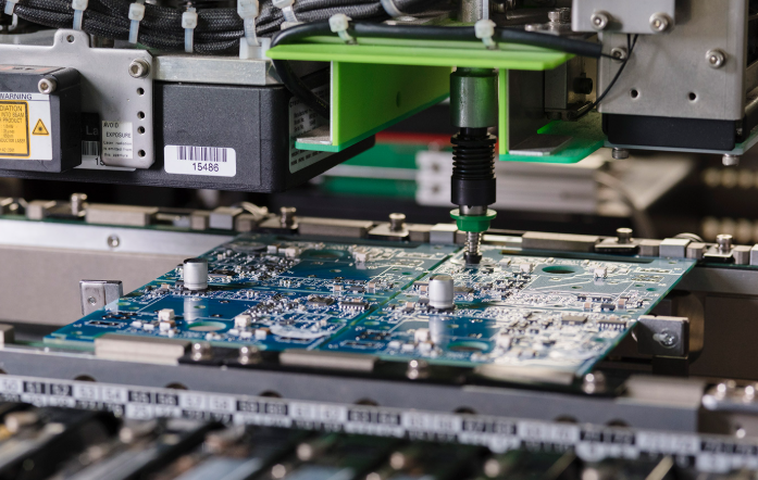
- Selective soldering: Delivers precision joints for sensitive components, avoiding thermal damage to nearby parts and ensuring consistent solder quality for critical connections.
- BGA rework and repair: Specialized service for ball grid array components, including reflow, reballing and defect correction using X-ray inspection for accuracy.
- Mixed-technology assembly: Combines SMT and through-hole processes to accommodate designs with both compact surface-mount parts and rugged through-hole components.
- Conformal coating: Protective layer application to shield PCBs from moisture, dust, chemicals and environmental stress, enhancing long-term reliability.
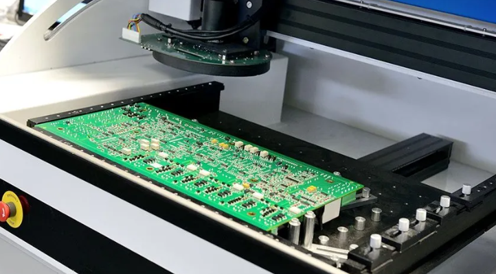
- Functional testing: Post-assembly validation to ensure PCBs perform as designed, identifying electrical or performance issues before final delivery.
- Box-build assembly: End-to-end integration service, combining PCBs with enclosures, wiring and other components to deliver fully assembled finished products.
Top 10 Best PCB Assembly India Manufacturer in India
| Company Name | Main Business | Core Advantage | PCBA Capability | Lead Time |
| EBest Circuit Co., Limited (Best Technology) | PCB design, prototyping, manufacturing and assembly | 20 years of experience, ISO 9001/13485/IATF16949 certified, 24/7 support | SMT, through-hole, heavy copper PCB assembly, complex high-end PCBs | Urgent orders 24 hours, standard 5-10 days (97.2% on-time delivery) |
| Roots EMS | PCB assembly, SMT services, mechatronics manufacturing | 50+ years of experience, IPC 610 Class 2/3 compliance, automated inspection | Fine pitch SMT, through-hole, box build, BGA rework, functional testing | Prototypes 3-5 days, volume production 7-15 days |
| Genus Electrotech Ltd. | Bare board PCBs, PCB assembly, corrugation products | ISO 9001:2015/14001:2015 certified, 72,000 sqm production area | Single/double-sided, multilayer PCBA, automotive/consumer electronics focus | Standard 10-15 days, bulk 15-20 days |
| Ascent Circuits Pvt. Ltd. | High-quality PCB manufacturing and assembly | Fully automated facility, RF/flexible PCB expertise | Multilayer PCBA, RF PCB assembly, SMT/through-hole | Prototypes 4-6 days, volume 8-12 days |
| AT&S India Pvt. Ltd. | High-end PCB/substrate manufacturing, assembly | HDI/semiconductor substrate expertise, 2.5D technology | High-density interconnect PCBA, rigid/flex PCBA, IC substrate assembly | High-end 15-25 days, prototypes 7-10 days |
| Shogini Techno Arts Pvt. Ltd. | PCB manufacturing for LED/automotive | 200,000 sqm monthly capacity, metal clad PCB specialization | 1-8 layer PCBA, metal clad assembly, SMT for LED | Standard 8-12 days, automotive 12-18 days |
| Circuit Systems India Ltd. | PCB layout, fabrication, prototyping and assembly | End-to-end technical support, custom design solutions | Prototype/low-volume PCBA, mixed-technology assembly | Prototypes 2-4 days, small-batch 5-8 days |
| Pul Raj Electronics | PCB manufacturing, assembly, custom fabrication | RoHS compliant, ESD-safe facilities, ISO 9001:2015 certified | SMT assembly, through-hole, rapid prototyping for IoT | Prototypes 3-5 days, standard 7-14 days |
| CIPSA-TEC India Pvt. Ltd. | PCB manufacturing, SMT/DIP assembly | Integrated SMT/DIP lines, cost-effective mass production | High-volume SMT, DIP soldering, quality inspection | Bulk 10-16 days, expedited 5-7 days |
| Zetwerk Electronics | PCB assembly, electronics manufacturing services | Government incentive access, global supply chain integration | Automotive/telecom PCBA, SMT, functional testing | Standard 8-13 days, automotive 14-20 days |
How to Choose the Best PCB Assembly India Service?
Selection Guide to Best PCB Assembly India Service:
- Verify core certifications: Prioritize PCB assembly companies in India with ISO 9001:2015 (98% of reputable providers hold this), IATF 16949 for automotive projects (mandatory for tier-1 suppliers), and ISO 13485 for medical applications (requires 100% compliance with regulatory documentation).
- Assess technical capabilities quantitatively: Confirm SMT precision (supports 01005-sized components), multilayer assembly capacity (up to 40 layers for high-end needs), and BGA rework capability (handles down to 0.4mm pitch with ≥99.5% success rate).
- Validate industry-specific experience: Check for at least 3+ completed projects in your field, with a minimum 2-year collaboration history with clients of similar scale, and a portfolio showing 70%+ of revenue from your target industry.
- Evaluate quality control processes with metrics: Ensure AOI inspection coverage (100% of SMT solder joint), X-ray inspection for BGA (detects voids ≥25% of pad area), and functional testing protocols that maintain a defect rate (DPPM) ≤50, a benchmark for top-tier manufacturers.
- Ensure full traceability: Verify MES-driven systems that track component batches, production workflows, test data, and shipments, with 100% unit-level traceability. Data must be retrievable for 3+ years (5 years for medical per MDR) and compliant with automotive UN R156 norms.
- Review reliability metrics from independent sources: Aim for on-time delivery rates ≥98% (industry average is 90%), customer satisfaction scores ≥4.5/5 on third-party platforms, and a customer retention rate of 85%+ for long-term partnerships.
- Confirm order volume flexibility: Validate prototype capacity (minimum 1-50 units with 3-5 day lead time) and high-volume scalability (monthly output ≥100,000 units), with order change response time ≤48 hours for mid-production adjustments.
- Assess post-delivery support: Ensure a minimum 1-year warranty (extendable to 3 years for medical/automotive), defect response time ≤8 hours, and a rework/repair completion rate of 95% within 5 working days.
How to Evaluate the Assembly Capability of PCB Assembly India?
Evaluation Guide to Assembly Capability of PCB Assembly India:
- Review equipment specifications: Verify high-precision pick-and-place machines (accuracy ±0.03mm, supporting 01005 size components), 3D SPI (solder paste inspection, height deviation tolerance ≤5%), and X-ray inspection equipment (BGA void and solder joint detection resolution ≥5μm).
- Verify compliance with IPC-A-610 standard: Confirm compliance with the corresponding class (Class 1 for consumer products, Class 2 for industrial products, Class 3 for medical/automotive products), and provide annual audit documents. All technicians hold IPC-A-610 training certificates.
- Evaluate professional material handling capabilities: Check proficiency in thick copper (2-20 oz) PCB assembly, ceramic substrate processing (high temperature resistance ≥150℃), and flexible/rigid-flex PCB assembly (minimum bending radius ≤10mm).
- Analyze First Pass Yield (FPY) metrics: Top Indian PCB assembly suppliers achieve a standard SMT assembly FPY ≥98%, and complex designs (20+ layers, 0.4mm pitch BGA) FPY ≥95%, while the industry average is 92%.
- Confirm Design for Manufacturability (DFM) support capabilities: Ensure DFM feedback is provided within 24-48 hours, covering solder mask optimization, component layout, and test point design, reducing rework rates by ≥30%.
- Verify traceability system robustness: Verify the traceability system integrated with MES (using barcodes/QR codes for each unit), covering component batches, production stations, test data, and shipping information, with data retained for 3-5 years (compliant with UN R156 and MDR standards).
How to Evaluate the Delivery Time of PCB Assembly Companies in India?
Evaluation Guide to Delivery Time of PCB Assembly Companies in India:
- Benchmark standard lead times against industry norms: 5-10 days for standard PCBA (batch 500-5000 pieces) and 15-20 days for HDI boards (8 layers or more) in PCB assembly in India, with top providers able to compress standard timelines by 20%-30%.
- Assess emergency order capacity: Verify 24-48 hour expedited service availability for prototypes (1-100 pieces), with clear scope (excludes custom components) and cost premium (15%-30% above standard rates) in writing.
- Validate MES system functionality: Ensure real-time tracking covers order status, process progress and quality checkpoints, with data synced every 2 hours and accessible via client portal for full transparency.
- Evaluate production buffer capacity: Aim for 15%-25% redundancy (industry best practice) in equipment and workforce, to absorb demand fluctuations without delaying existing orders.
- Review on-time delivery (OTD) metrics: Prioritize providers with OTD ≥98% (industry average 90%) over 6-12 months, backed by third-party audit reports, and penalty clauses (0.5%-1%/day) for delays.
- Confirm material sourcing stability: Check dual-supplier certification for key components, ≥60% local sourcing rate for common parts, and 72-hour contingency plans for component shortages.
How Much Does PCB Assembly India Cost?
- Component Costs: Bulk purchases (over 10,000 units) typically receive an 8%-15% discount. Lead-free components are 5%-10% more expensive than leaded components, while specialized parts (e.g., RF components, military-grade chips) command a 20%-40% price premium due to limited supply.
- Assembly Labor Costs: SMT assembly costs $0.02-$0.05 per component, while through-hole assembly (manual insertion) costs 30%-50% more. High-precision requirements (01005 components, 0.4 mm pitch BGA) add a 15%-25% labor surcharge.
- Setup Fees: One-time fees include $50-$200 for stencil fabrication (depending on size/layers) and $100-$300 for programming/production line setup. Orders exceeding 5,000 units typically receive a 50%-70% discount on setup fees.
- Testing Costs: AOI inspection costs $0.10-$0.30 per unit, X-ray inspection for BGAs costs $0.50-$1.00 per unit, and functional testing costs vary from $1-$5 per unit depending on complexity (Level 3 medical/automotive products require higher testing costs).
- Material Loss: Prototype products have a loss rate of 3%-5% (standard for small-batch production), while mass production (over 10,000 units) uses automated processes, keeping the loss rate at 1%-2%. High-cost materials (e.g., ceramic substrates) have a maximum loss rate of 1%.
- Logistics and Taxes: The Goods and Services Tax (GST) for electronics in India is 18%, and local logistics costs account for 5%-8% of the total cost. Seasonal factors (e.g., monsoons) may necessitate air freight, increasing logistics costs by 15%-20%.
- Volume Discounts: We offer tiered pricing – 5%-8% discount for 10,000-50,000 units, 8%-12% discount for 50,000-100,000 units, and 12%-15% discount for over 100,000 units. Discounts typically include component procurement and assembly.
Future Challenges for PCB Assembly in India
- High-end material dependence: Over 80% of advanced substrates (e.g., HDI, semiconductor substrates) rely on imports from Japan and South Korea, leading to 15%-30% cost premiums and supply delays for premium PCB assembly in India projects.
- Skill gaps: Shortage of talent proficient in HDI (20+ layers) and semiconductor packaging assembly results in 10%-15% lower first-pass yields, with only 35% of workforce trained in next-gen assembly processes.
- Supply chain volatility: Global chip shortages and geopolitical trade frictions (e.g., 2025 India anti-dumping probe on PCB drills) disrupt component sourcing, causing 10-20 day production delays for 40% of manufacturers.
- Technology upgrade costs: Next-gen SMT placement machines and 3D X-ray inspection equipment cost $500k-$1.2M per unit, straining small-to-mid-sized PCB assembly companies in India with limited capital reserves.
- Policy uncertainty: Frequent adjustments to PLI scheme subsidies (10%-25% fluctuations) and import duty revisions (5%-12% tariff changes) force manufacturers to delay long-term facility expansion plans by 6-12 months.
- Environmental regulations: Stricter RoHS 3.0 and electronic waste norms increase compliance costs by 3%-5% of annual revenue, requiring investments in eco-friendly solder and waste treatment systems.
- Market competition: 25% annual growth in local and international players squeezes profit margins from 15%-18% to 8%-12%, pushing manufacturers to cut costs without compromising quality.
FAQs of PCB Manufacturing and Assembly India
Q1: What causes component lifting (tombstoning effect) in SMT assembly? How can it be resolved?
A1: Component lifting is caused by uneven thermal capacity of the solder pads, placement offset, or inconsistent reflow soldering temperatures. Solutions include optimizing pad design for thermal balance, calibrating the pick-and-place machine for improved accuracy, and fine-tuning the reflow soldering profile. It is recommended to collaborate with an Indian PCB assembly service provider using 3D SPI (three-dimensional solder paste inspection) to monitor solder paste application.
Q2: How to address PCB delamination during assembly?
A2: Delamination stems from moisture absorption in PCBs or rapid reflow temperature rises. Solutions involve pre-baking PCBs at 120°C for 4-8 hours before assembly, using high-TG materials (TG 170+) and controlling reflow temperature ramp rates.
Q3: Why do BGA solder voids occur and how to minimize them?
A3: Voids result from flux outgassing, improper solder paste volume or PCB warpage. Minimize by using low-void solder paste, optimizing reflow profiles for flux evaporation and ensuring PCB flatness. X-ray inspection post-assembly helps identify voids exceeding 25% of pad area for rework.
Q4: How to resolve component misalignment in high-volume SMT assembly?
A4: Misalignment is caused by worn placement machine nozzles, incorrect feeder setup or PCB warpage. Resolutions include regular nozzle calibration, feeder maintenance and using fixture supports for thin PCBs. Automated optical inspection (AOI) after placement catches misalignments before soldering.
Q5: What causes cold solder joints and how to prevent them?
A5: Cold joints arise from insufficient reflow temperature, short peak time or oxidized pads. Prevention involves validating reflow profiles to meet component specs, cleaning pads before assembly and using quality flux. Post-assembly functional testing identifies hidden cold joints affecting performance.