

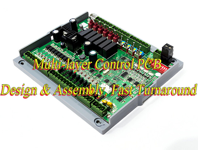
How to design multi-layer control PCB? Let’s explore benefits, applications, design technical parameter and guide, assembly process for multilayer control PCB.
Are you worried about these problems?
- How to address yield fluctuations caused by significant interlayer alignment errors?
- How to tackle frequent signal crosstalk under high-density routing scenarios?
- How to resolve thermal management challenges in multi-layer boards where heat dissipation efficiency fails to meet requirements?
As a multilayer control PCB manufacturer, EBest Circuit (Best Technology) can provide you service and solutions:
- Design Collaboration Optimization: Provide full-process design support from schematic to PCB layout, leveraging layer planning and impedance matching algorithms to proactively mitigate interlayer alignment risks and ensure first-board yield stability above 95%.
- Signal Integrity Specialization: For high-speed signal environments, implement balanced differential pair routing and dedicated power layer segmentation, paired with 3D simulation validation, to suppress crosstalk below 5% and guarantee signal transmission quality.
- Customized Thermal Management Solutions: Integrate material properties with thermal path design to develop stepped thermal conduction structures and concealed thermal pads, enhancing heat dissipation efficiency by 30% to meet high power density product demands.
Welcome to contact us if you have any request for multilayer control PCB: sales@bestpcbs.com.
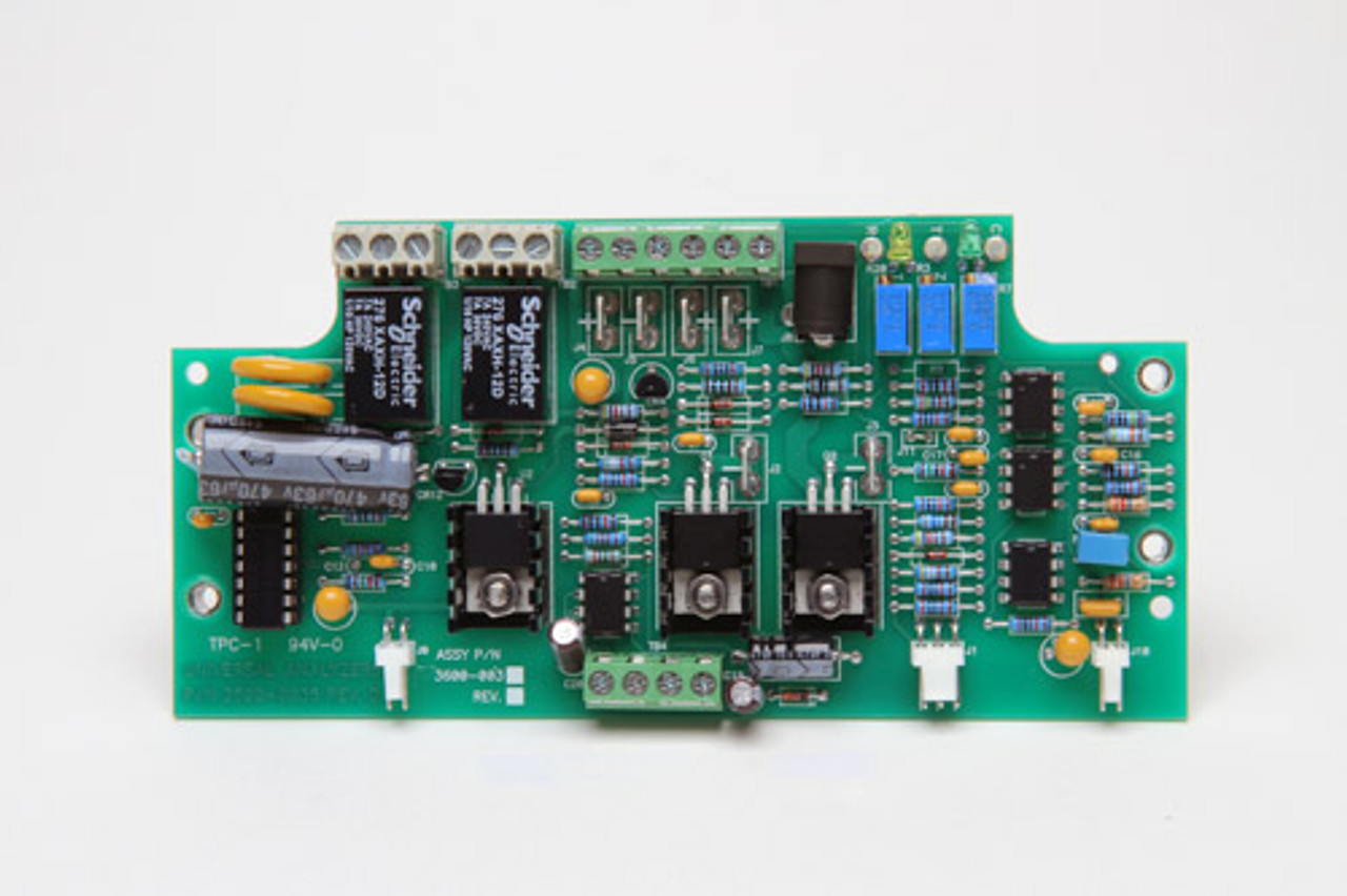
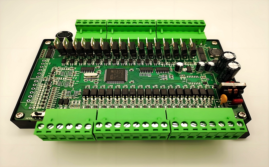
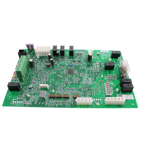
What Is Multi-layer Control PCB?
A multi-layer control PCB (printed circuit board) is a special-purpose circuit board with a three-layer or higher conductive layer structure. It integrates core electronic components such as microprocessors/controllers, memory, input/output interfaces, communication modules, and power management. It is specifically used as the execution carrier for core control functions in electronic systems, responsible for processing signals, executing logic, and driving external devices (such as sensors and actuators).
Advantages of Multilayer Control PCB
Benefits of multi-layer control PCB:
- High-Density Integration for Compact Design: Multilayer stack-up technology enables complex circuit integration within limited space (e.g., 4+ layer PCBs supporting BGA/QFN packaging), reducing surface trace density by over 60%. Ideal for size-sensitive products like smartphones and portable medical devices, it achieves 20%-30% weight reduction and enhances market competitiveness.
- Signal Integrity Optimization for High-Speed Transmission: Dedicated power and ground planes form low-impedance return paths, paired with impedance control (e.g., 50Ω RF line matching) to reduce signal crosstalk by over 40%. This ensures stable operation for PCIe 5.0/6.0, DDR5, and other high-speed interfaces, meeting strict requirements of AI servers and 5G base stations.
- Enhanced Electromagnetic Compatibility (EMC): Multilayer structure inherently acts as an EMI shield, combined with zoned power distribution and multi-point grounding to reduce electromagnetic radiation by over 50%. Compliant with IEC 61000-4-3 and other international EMC standards, it suits harsh environments like automotive ECUs and industrial control systems.
- Efficient Thermal Management: Internal copper layers and thermal materials (e.g., copper blocks) form a heat-dissipation network, with thermal vias reducing thermal resistance by over 30%. Suitable for high-power components (e.g., GPUs, power modules), it prevents thermal concentration failures and extends MTBF by over 50%.
- Modular Design Accelerates Development: Layered layouts enable independent routing of functional modules (power/signal/ground planes), paired with blind/buried vias and via-in-pad technology to minimize design iterations. For example, 6+ layer PCBs with resin plugging and electroplated caps shorten design verification cycles by 40%, reducing debugging costs.
- Enhanced Anti-Interference and Reliability: Multilayer dielectric and prepreg adhesives boost structural strength, doubling flexural strength and withstanding -40°C to 125°C temperature ranges. Protected inner-layer traces reduce physical damage risks, ideal for aerospace, defense, and other high-reliability applications.
- Cost Efficiency Optimization: While unit board costs are higher, overall BOM costs decrease by 15%-25% through reduced connectors and material waste. For example, SMT and HDI processes enhance manufacturing efficiency by over 30%, suitable for mass-produced consumer electronics and telecom equipment.
- Flexible Adaptation to Complex Topologies: Supports high-speed routing needs like differential pairs and serpentine length matching, compatible with SerDes, LVDS, and other standards. In industrial control systems, it enables real-time signal processing and anti-interference design for PLCs.
Typical Applications of Multi-layer Control PCB
Applications of multi-layer control PCB:
- Industrial Automation Control Systems: PLC Programmable Logic Controllers; Industrial Robot Control Units; CNC Machine Tool Control Systems; Production Line Automation Equipment.
- Automotive Electronic Control Systems: Engine Control Unit (ECU); Body Control Module (BCM); Autonomous Driving Control Systems; Battery Management System (BMS).
- Communication Equipment Control Modules: Base Station Controllers; Network Switch Control Boards; Router Main Control Units; 5G Communication Equipment Control Cores.
- Medical Equipment Control Systems: Medical Imaging Equipment Control Units; Vital Signs Monitoring Devices; Surgical Robot Control Systems.
- Medical Diagnostic Equipment Main Control Boards: Aerospace Control Systems; Flight Control Computers; Navigation System Control Units; Satellite Control Systems; UAV Flight Control Systems.
- Energy Management Systems: Smart Grid Control Terminals; Renewable Energy Controllers; Power Conversion Control Systems; Energy Dispatch Monitoring Units.
- High-End Consumer Electronics: High-End Gaming Console Motherboards; Smart Home Appliance Control Cores; VR/AR Device Control Boards; High-End Audio Control Systems.
Multi-layer Control PCB Design Technical Specifications
| Specific Parameter | Typical Value/Range |
| Layer Count | 4~36 layers |
| Material | FR-4, High-frequency Materials, Metal Substrate, etc. |
| Glass Transition Temperature (Tg) | ≥150°C (Recommended for Multilayer Boards) |
| Core Thickness | 0.10mm~1.0mm |
| Prepreg Type | 106/1080/2116/7628, etc. |
| Impedance Control | Single-ended 50Ω±10%, Differential 100Ω±10% |
| Dielectric Constant (Dk) | 3.6~4.5 (@1GHz) |
| Dissipation Factor (Df) | 0.019~0.025 (@1GHz) |
| Copper Thickness (Outer/Inner Layer) | 0.5~3oz (17~105μm) |
| Minimum Trace Width/Spacing | 3mil/3mil (0.076mm) |
| Minimum Hole Size | 0.1mm |
| Board Thickness & Tolerance | 0.4~5.4mm (±0.1mm or ±10%) |
| Surface Finish | ENIG, HASL, OSP, etc. |
| Interlayer Dielectric Thickness | 2~8mil (Core Layer) |
| Reference Plane Design | Adjacent Power/Ground Plane |
| Differential Pair Symmetry | Width/Spacing Error <10% |
Multi-layer Control PCB Design Guide
Below is a guide to multi-layer control PCB design:
1. Layer Stackup Design & Material Selection
- Layer Count Optimization: Balance signal/power layers based on routing density and signal integrity requirements (e.g., 4-layer for simple control boards, 8-12+ layers for high-speed/mixed-signal designs).
- Core & Prepreg Materials: Use FR-4 (standard) or high-Tg/low-Dk materials (e.g., Rogers 4350B, Isola 370HR) for high-temperature/high-frequency applications. Specify copper thickness (e.g., 1/2 oz, 1 oz, 2 oz) based on current-carrying needs and thermal dissipation.
- Symmetrical Stackup: Ensure balanced dielectric thickness between layers to minimize warpage (e.g., L2-L3 power/ground, L4-L5 signal layers).
- Buried/Blind Vias: Use for high-density interconnects (HDI), with clear design rules for aspect ratio (<8:1 for reliable plating) and layer registration.
2. Signal Integrity (SI) & Power Integrity (PI)
Impedance Control: Define trace width/spacing for 50Ω (differential pairs: 100Ω) using tools like Saturn PCB Toolkit or Altium’s SI Calculator. Maintain consistent impedance across layers via controlled dielectric height.
Crosstalk Mitigation: Route critical signals (e.g., clocks, DDR) on inner layers with adjacent ground planes. Use 3W rule (trace spacing ≥ 3× trace width) or guard traces to reduce coupling.
Power Distribution Network (PDN):
- Dedicate power/ground planes (e.g., split planes for analog/digital domains).
- Place decoupling capacitors (0.1μF ceramic for high-frequency, 10μF electrolytic for bulk) near IC power pins, with low-inductance connections.
- Use plane stitching vias (e.g., 10-mil via spacing) to connect ground planes and reduce loop inductance.
Return Path Management: Ensure continuous ground paths under high-speed signals to minimize EMI (e.g., avoid splitting ground planes under differential pairs).
3. Thermal Management
- Thermal Vias & Copper Pours: Use thermal vias (e.g., 12-mil via arrays) under power devices to transfer heat to inner/outer layers. Add copper pours (≥20mil trace width) on top/bottom layers for heat dissipation.
- Component Placement: Position heat-generating components (e.g., MOSFETs, processors) near thermal vias or exposed pads. Maintain clearance for airflow in enclosures.
- Thermal Simulation: Validate thermal performance using tools like Ansys Icepak or Altium Thermal Simulator, ensuring ΔT < 30°C above ambient.
4. High-Speed & Mixed-Signal Design
- Routing for High-Speed Signals: Use controlled-impedance microstrips or striplines. Avoid 90° bends; use 45° or curved traces to reduce reflections.
- Analog/Digital Isolation: Segment ground planes (e.g., AGND, DGND) and connect at a single point (star ground) to prevent noise coupling. Use ferrite beads or inductors for isolation.
- DDR/LVDS Routing: Follow length-matching rules (±5mil skew for DDR3/4) and via-in-pad for BGA packages. Use ground planes under signal layers for shielding.
5. Manufacturing & Assembly Considerations
Design for Manufacturing (DFM):
- Adhere to IPC-6012 standards for minimum line/space (e.g., 4mil/4mil for 6-layer boards), via size (10mil drill with 20mil pad), and annular ring (≥6mil).
- Specify surface finish (e.g., ENIG for fine-pitch components, HASL for cost-sensitive designs).
Testability: Include fiducials for automated assembly, test points for in-circuit testing, and boundary-scan (JTAG) support.
Panelization: Define panel dimensions, tooling strips, and scoring/V-cut lines for efficient fabrication.
6. EMI/EMC Compliance
- Shielding & Grounding: Use grounded shields (e.g., copper tape, ferrite sheets) for sensitive circuits. Ensure chassis ground connections for shielding effectiveness.
- Filtering: Add common-mode chokes, X/Y capacitors, and transient voltage suppressors (TVS) on I/O lines.
- Compliance Testing: Plan for pre-compliance testing (e.g., near-field scans, conducted emissions) to identify issues early.
7. Documentation & Collaboration
- Design Deliverables: Provide complete fabrication drawings (Gerber files), assembly drawings (BOM, pick-and-place), and SI/PI reports.
- Version Control: Use revision-controlled design tools (e.g., Altium 365, Cadence Allegro) to track changes.
- Collaboration: Share design reviews with manufacturers and cross-functional teams (e.g., mechanical, firmware) to ensure alignment.
Multi-layer Control PCB Assembly Processes
Here are processes about multi-layer control PCB assembly:
1. Inner Layer Circuit Fabrication and Pretreatment
- Board Cutting and Cleaning: Cut copper-clad laminate substrates according to design specifications. Remove surface oil and oxides through acid washing and brushing to ensure copper foil adhesion.
- Dry Film Lamination: Apply photosensitive dry film (thickness 15-30μm) to the cleaned substrate. Secure it via hot pressing or vacuum adsorption as a medium for pattern transfer.
- Exposure and Development: Use LDI (Laser Direct Imaging) or conventional exposure machines. UV light cures specific areas of the dry film. Unexposed sections dissolve in developer solution to form inner layer circuit patterns.
- Etching and Film Removal: Etch unprotected copper using acidic/alkaline solutions to create precise circuits. Remove residual dry film to expose the copper circuitry.
2. Inner Layer Quality Inspection and Repair
- AOI Optical Inspection: Scan circuits with high-resolution cameras. Compare with golden samples to detect defects like opens, shorts, and line width deviations.
- VRS Manual Repair: Address defects (e.g., gaps, dents) using gold wire soldering or conductive adhesive to ensure electrical continuity.
- Brown Oxidation Treatment: Chemically oxidize the copper surface to form a honeycomb Cu₂O/CuO layer (thickness 0.2-0.5μm) for enhanced bonding with prepreg.
3. Lamination and Molding Process
- Layer Stack Configuration: Stack inner layers, prepreg sheets (PP), and outer copper foils in design order. Use alignment pins to ensure interlayer accuracy (±0.05mm).
- Vacuum Hot Pressing: In a vacuum press, apply 170-200°C heat and 2-4MPa pressure. Melt and cure epoxy resin in prepreg to bond the multilayer structure.
- Symmetry Control: Ensure balanced material distribution on both sides to prevent warpage. Uniform copper distribution affects final thickness consistency.
4. Drilling and Hole Metallization
- Precision Drilling: Use CNC drilling machines (60-100krpm) to create through-holes/blind holes. Tightly control hole diameter tolerance (±0.05mm) and ensure smooth walls without burrs.
- Desmearing and Chemical Copper Plating: Remove drilling residues with swelling agents. Deposit a 0.3-0.8μm conductive layer via electroless copper plating.
- Full-Board Copper Plating: Thicken the hole copper layer to ≥25μm using sulfuric acid copper plating (current density 1.5-3A/dm²) for reliable electrical connections.
5. Outer Layer Circuit Fabrication and Surface Treatment
- Outer Layer Pattern Transfer: Repeat inner layer processes to form outer circuits via lamination, exposure, and development. Use positive-tone processes to protect non-circuit areas.
- Pattern Plating and Etching: Plate copper/tin, etch unprotected copper, and strip tin to finalize outer circuits.
- Solder Mask and Legend Printing: Apply solder mask ink (20-40μm thickness) and expose it to form protective layers. Print legends via screen printing (tolerance ±0.1mm).
- Surface Finishing: Choose ENIG (for solderability), OSP (organic solderability preservative), or HASL (hot air solder leveling) based on requirements. Prevent copper oxidation and enhance solderability.
6. Final Inspection and Reliability Verification
- Electrical Performance Testing: Verify circuit continuity and impedance with flying probe testers. Use vector network analyzers for high-speed signal integrity checks.
- X-Ray Inspection: Penetrate layers to inspect blind hole alignment, solder joint quality (e.g., BGA packages), and detect voids/bridging.
- Environmental Reliability Testing: Include thermal shock (-55°C to 125°C cycling), moisture sensitivity level (MSL) tests, and vibration simulations (transport/usage environments).
- Functional Verification: Use ATE (automated test equipment) for power testing and signal integrity checks to ensure circuits meet design specifications.
7. Packaging and Delivery
- Profile Cutting: Shape boards to customer dimensions via routing machines. Ensure smooth edges without burrs.
- FQC Final Inspection: Combine manual visual checks and AOI sampling to confirm no cosmetic defects, contamination, or labeling errors.
- Vacuum Packaging: Package boards in moisture-resistant, dust-proof materials for stable quality during transit. Deliver to customers.
Why Choose EBest Circuit (Best Technology) as Control PCB Assembly Manufacturer?
Reasons why choose us as control PCB assembly manufacturer:
- 19 Years of PCBA Assembly Expertise: Leveraging 19 years of industry experience, we have served over 5,000 global enterprises across sectors from consumer electronics to industrial control, ensuring each PCB undergoes proven, mature processes.
- Rapid Delivery for Market Advantage: Our intelligent production scheduling and optimized workflows enable standard components to be delivered in 3 days and complex multilayer boards in 7 days, 30% faster than industry averages, helping clients seize market opportunities.
- Flexible Small-Batch Assembly Support: We accommodate small-batch production starting from 1 unit, reducing upfront costs for R&D prototyping and custom product validation, enabling seamless transitions from prototype to mass production.
- End-to-End Quality Control System: From material intake to final inspection, our 12-stage quality gates integrate AOI optical inspection, X-ray analysis, and electrical testing to achieve a defect rate of ≤0.01%, exceeding industry standards.
- Material Compatibility Expertise: We specialize in hybrid lamination techniques for high-frequency materials (e.g., PTFE, hydrocarbon resins) and conventional FR4, offering end-to-end solutions from material selection to process parameter optimization.
- Eco-Friendly Surface Finishing Options: Our portfolio includes ENIG, OSP, and chemical nickel gold treatments, all compliant with RoHS and REACH standards, ensuring global market access without compromising performance.
- Tailored Value-Added Services: From DFM (Design for Manufacturing) analysis to functional testing, our dedicated engineering team provides one-on-one technical support to accelerate time-to-market.
- Optimized Cost Efficiency: Through process refinement and economies of scale, we maintain quality while reducing overall costs by 15% compared to competitors, enhancing client profitability.
Our PCB Assembly Capabilities
| Item | Capabilities |
| Placer Speed | 13,200,000 chips/day |
| Bare Board Size | 0.2 x 0.2 inches – 20 x 20 inches/ 22*47.5 inches |
| Minimum SMD Component | 01005 |
| Minimum BGA Pitch | 0.25mm |
| Maximum Components | 50*150mm |
| Assembly Type | SMT, THT, Mixed assembly |
| Component Package | Reels, Cut Tape, Tube, Tray, Loose Parts |
| Lead Time | 1 – 5 days |
How to Get a Quote for Multilayer Control PCB Project?
All files need to be submitted to get a quote for multilayer control PCB project:
- Core Design Files: Gerber Files (including routing layers, solder mask layers, silkscreen layers), Drill Files (hole diameter, hole position data), Bill of Materials (BOM) (component names, models, quantities, specifications, suppliers).
- Technical Parameters Documentation: Layer count, board thickness, copper thickness, solder mask color, surface finish (e.g., HASL, ENIG), special process requirements (e.g., high-frequency materials, thick copper design).
- Supporting Materials: Circuit schematic, PCB engineering drawing (including dimension annotations, material types), sample (for design validation), process requirement documents (e.g., soldering temperature, testing standards).
- Mass Production Requirements: Production quantity, delivery time, packaging specifications (e.g., anti-static packaging), shipping method.
- Additional Documents: Contract draft, quality agreement, special testing requirements (e.g., signal integrity testing, reliability testing).
Welcome to contact us if you have any request for multilayer control PCB: sales@bestpcbs.com.