

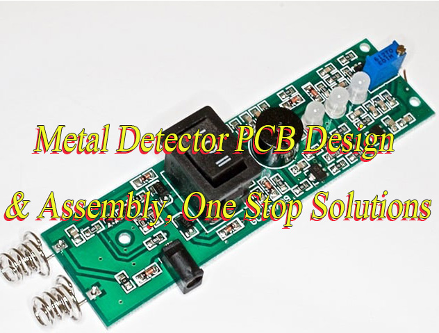
What is metal detector PCB? Let’s discover its types, applications, design consideration, layout techniques, assembly process through this blog.
Are you worried about these problems?
- Does your metal detector consistently suffer from unstable detection accuracy due to PCB noise interference?
- Does small-batch, multi-version PCB assembly lead to delivery delays and uncontrolled costs?
- When encountering EMC test failures, can you quickly pinpoint whether the issue lies with the PCB design or the assembly process?
As a metal detector PCB assembly manufacturer, EBest Circuit (Best Technology) can provide you service and solutions:
- Precise Impedance Control Service: Utilizing a four-layer PCB immersion gold process + signal integrity analysis, we reduce background noise at its source, ensuring even weak metal signals are detected.
- Flexible Production System: We build modular production lines supporting flexible production capacity from 50 to 5000 pieces, enabling rapid response to design changes and reducing average delivery time by 30%.
- End-to-End Technical Collaboration: We provide end-to-end support from design review and DFM analysis to EMC pre-testing, accurately pinpointing problem areas and providing data-driven rectification solutions.
Welcome to contact us if you have any inquiry for metal detector PCB design and assembly: sales@bestpcbs.com.
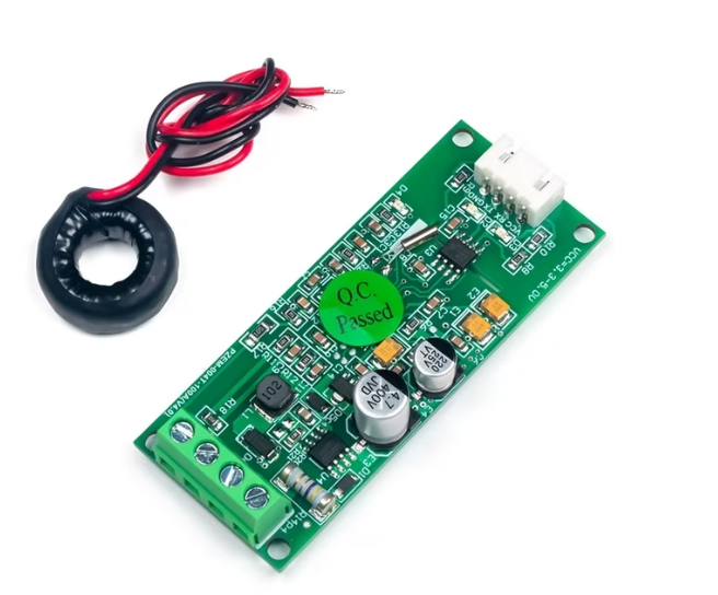
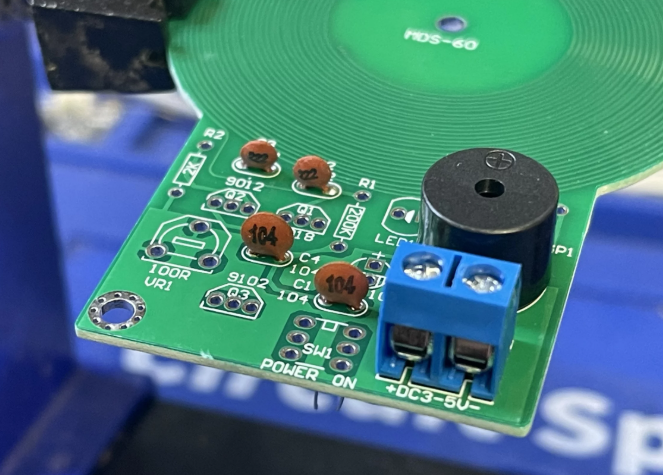
What Is Metal Detector PCB?
A metal detector PCB is a printed circuit board specifically designed for metal detection equipment. It integrates an electromagnetic induction or pulse induction core module, using an onboard detection coil (such as an LC oscillator inductor) to sense the eddy current effect or frequency shift caused by metal. This triggers a signal processing circuit (including amplification, filtering, and a microcontroller) to analyze the signal changes, ultimately driving output components such as LEDs/buzzers to achieve the alarm function.
Its design requires precise impedance matching, optimized wiring to suppress electromagnetic interference, and consideration of sensitivity adjustment and power supply stability to ensure reliable detection of metal targets in complex environments. It is suitable for professional scenarios such as security inspection, industrial non-destructive testing, and treasure hunting equipment.
Types of Metal Detector Circuit Board
| Type | Technical Features | Application Scenarios |
| VLF PCB (Very Low Frequency) | Dual-coil (transmitter/receiver) system that detects metals through frequency differences | Commercial treasure hunting, security screening, archaeology |
| PI PCB (Pulse Induction) | Single-coil alternating transmitter/receiver pulses that detect magnetic field decay | Deep detection, mineralized soil environments |
| BFO PCB (Beat Frequency Oscillator) | Two oscillators with close frequencies that detect metals through beat frequency | Simple metal detectors, entry-level equipment |
Applications of Metal Detector PCB Board
- Security checks: Personnel and baggage security checks at airports, train stations, and customs.
- Industrial inspection: Metal impurity detection in the food, pharmaceutical, and textile industries.
- Underground exploration: Archaeological excavation, treasure hunting, underground pipeline/cable location.
- Military security: Mine detection, border monitoring.
- Medical field: Surgical instrument location, prosthetic limb inspection.
Metal Detector PCB Design Considerations
Below are main considerations for metal detector PCB design:
Electromagnetic Compatibility (EMC) Optimization Design
- Minimize loop area: Signal lines and power loops must strictly follow the “short, straight, close” principle. Critical signal lines (e.g., clocks, differential pairs) should use 45° arc routing instead of 90° right angles. Multilayer boards require a complete ground plane with signal layers adjacent to ground layers to reduce electromagnetic radiation and crosstalk.
- Grounding strategy: High-frequency circuits adopt multi-point grounding (e.g., switching power modules), while low-frequency analog circuits use single-point grounding. Digital and analog grounds connect via ferrite beads or 0Ω resistors at a single point to avoid ground loop noise. Sensitive areas (e.g., preamplifiers) require isolated ground planes.
- Filtering and shielding: Power entry points use common-mode chokes with X/Y capacitor filter networks. Transmitter coil drive circuits are enclosed in metal shields with 360° equipotential grounding. High-speed signal lines (e.g., LVDS) employ ground wrapping, and adjacent layer routing directions are perpendicular to minimize coupling.
Signal Chain and Coil Layout Precision Control
- Balanced receiver coil design: Triple-coil structure (central transmitter + dual symmetric receivers) ensures zero differential voltage in absence of metal. Coil windings must be symmetrically distributed with wire diameter and turn count accuracy ≤1% to prevent temperature drift-induced false triggers.
- Signal chain layout: Low-Noise Amplifier (LNA) is placed adjacent to receiver coils to minimize signal path loss. Filter capacitors (e.g., 10μF tantalum + 0.1μF C0G) must be near op-amp power pins. Differential signal lines maintain equal length (error ≤5mil) with matched impedance (typically 50Ω) to avoid timing skew.
- Coil electrical optimization: Transmitter coils use Litz wire to reduce skin effect. Coil inductance is validated via simulation (e.g., ANSYS HFSS) to ensure precise resonance frequency (10kHz-1MHz) matching with tuning capacitors, enhancing detection sensitivity.
Power Integrity (PI) and Low-Noise Design
- Low-noise power architecture: Digital circuits use LDOs (e.g., 1μVrms ultra-low noise types), while analog circuits employ DC-DC + LC filtering (e.g., 22μF electrolyytic + 0.01μF C0G). Avoid coupling switching noise to sensitive circuits; consider Silent Switcher or synchronous rectification.
- Decoupling strategy: IC power pins require 10nF–100nF high-frequency decoupling capacitors (distance ≤3mm). Board-level power traces use ≥18mil wide copper to reduce voltage drop. Critical nodes (e.g., ADC references) add π-type filters to suppress power ripple below 1mV.
Thermal Management and Reliability Design
- Thermal distribution balance: High-power components (e.g., MOSFETs, power inductors) are evenly distributed to prevent hotspots. High-dissipation areas use thermal copper or pads connected via via arrays to bottom-layer thermal pads. Temperature-sensitive components (e.g., crystals) are placed away from heat sources.
- Material selection: Substrates use high-Tg (≥170°C) FR4 or Rogers high-frequency materials for dimensional stability under high temperatures. Surface finishes prioritize HASL lead-free processes meeting RoHS/REACH standards. Critical pads use ENIG for improved soldering reliability.
Manufacturability and Standardization Compliance
- Layout specifications: Components are grouped by function (digital/analog/power), with sensitive devices (e.g., ADCs, op-amps) kept away from I/O interfaces. SMT pads and vias maintain ≥25mil spacing to avoid solder wicking. Process edges reserve ≥3mm for automated pick-and-place machines.
- Regulatory compliance: Designs adhere to IPC-6012 Class 2/3 standards and pass CE/FCC EMC certifications. Critical parameters (e.g., impedance, tolerances) include tolerance ranges (±5%) to prevent out-of-spec usage. Documentation includes BOM lists, Gerber files, and process specifications.
Metal Detector PCB Layout Techniques
1. Signal Path Optimization and Impedance Control
- Short and Direct Routing Principle: High-frequency signal paths (e.g., oscillator, amplifier links) must adopt the shortest linear routes, avoiding 90° right-angle bends. Prefer 45° oblique lines or curved traces to minimize signal reflection and crosstalk. For instance, LC resonant circuit input/output path lengths should be strictly controlled within λ/10 (λ denotes wavelength at operating frequency).
- Impedance Matching Design: High-frequency signal lines (e.g., 50Ω microstrip) require precise calculation and verification via PCB stack-up parameters (copper thickness, dielectric constant, interlayer spacing). Time Domain Reflectometry (TDR) measurements must confirm impedance deviation ≤±10%. Sensitive analog signals (e.g., preamplifier outputs) should use differential pairs to suppress common-mode noise.
- Interlayer Transition Specification: Cross-layer signal connections via vias must employ “back-drilling” to reduce stub effects. High-speed signal vias should have a hole diameter ≤0.3mm and spacing ≥2× hole diameter to prevent signal integrity degradation.
2. Power Integrity Management
- Decoupling Capacitor Placement: Low-ESR ceramic capacitors (e.g., 0.1μF/100nF) should be positioned ≤5mm from power pins, complemented by bulk electrolytic capacitors (e.g., 10μF) for multi-stage filtering. Capacitors must be arranged from high-frequency to low-frequency outward to avoid coupling power noise into sensitive analog circuits.
- Power Plane Segmentation: Digital power (e.g., MCU supply) and analog power (e.g., preamplifier) require physical isolation (e.g., split lines, moats) or dedicated power planes to mitigate digital noise impact on analog front-ends. Multi-layer boards should adopt a “star” power distribution network (PDN) to reduce power impedance.
3. Electromagnetic Compatibility (EMC) Enhancement
- Shielding and Grounding Design: High-frequency modules (e.g., oscillators, drivers) should be surrounded by copper shields connected to ground planes via via arrays to form Faraday cages. Ground planes must remain intact without breaks to prevent ground bounce. Sensitive circuits (e.g., VCOs) must avoid placement beneath high-speed digital traces.
- Filter Application: LC filters or ferrite beads should be added at power inputs and signal interfaces to suppress high-frequency noise. Coil leads should use twisted pairs or coaxial cables to minimize external EMI.
- Differential Signal Handling: Critical digital interfaces (e.g., SPI, I²C) should employ differential signaling with common-mode chokes to enhance noise immunity.
4. Component Placement and Thermal Management
- Functional Partitioning: Layout follows “analog-digital-power” partitioning. Analog front-ends (e.g., preamplifiers, filters) should be isolated from digital circuits (e.g., MCUs, LED drivers). High-frequency coils must maintain ≥2mm clearance from PCB edges to avoid edge effects impacting detection sensitivity.
- Thermal Design Optimization: High-power components (e.g., power amplifiers, DC-DC converters) should have copper thermal layers beneath them, connected to backside heat sinks via via arrays. Thermal components should be spaced ≥3mm apart to prevent thermal coupling-induced performance drift.
- Coil Design Specification: Detection coils should use multi-strand enameled wire to reduce skin effect. Coil leads must adopt “star” grounding to minimize loop area and enhance noise immunity.
5. Manufacturing Feasibility and DFM (Design for Manufacturing)
- Process Compatibility: Minimum trace width/spacing ≥6mil (adjustable per fabricator capability), copper thickness 1-2oz (1oz recommended for high-frequency circuits to minimize skin loss). Pad dimensions must match component packages (e.g., QFN, 0603) to prevent solder joint defects.
- Test Point Design: Critical nodes (e.g., power, signal outputs) should include test probe points spaced ≥2.54mm for test fixtures. “Teardrop” routing strengthens pad-to-trace connections.
- Material Selection: High-frequency circuits should use low-loss substrates (e.g., Panasonic M6 FR-4, Rogers 4350B) to reduce signal attenuation. Surface finishes like ENIG (Electroless Nickel Immersion Gold) improve soldering reliability.
Metal Detector PCB Assembly Process
A detailed guide to metal detector PCB assembly:
1. Material Preparation and Preprocessing
- Component List Verification: Cross-check all components (MCU, inductor coils, capacitors, resistors, LEDs, buzzers) against the BOM list to ensure models, voltage ratings, and package dimensions comply with German/European (IEC 60115) or US standards (IPC J-STD-001).
- PCB Substrate Inspection: Verify PCB boards are free of oxidation, scratches, or lamination defects. Use AOI (Automated Optical Inspection) equipment to scan for micro-shorts, opens, and pad dimension deviations.
- Preprocessing: Pre-form or tin-plate leads of components requiring special handling (e.g., high-power resistors, HF inductors) to ensure soldering reliability.
2. SMT Placement and Reflow Soldering
- Solder Paste Printing: Utilize high-precision stencil printers to control paste thickness (typically 0.12–0.15mm). Validate print quality via SPI (Solder Paste Inspection) to eliminate bridging or insufficient solder defects.
- Component Placement: Employ high-speed placement machines (e.g., Siemens SIPLACE series) to mount components per coordinate files, prioritizing small-size parts (e.g., 0402 capacitors, 0603 resistors) followed by larger packages (e.g., QFP-packaged MCUs).
- Reflow Soldering: Implement nitrogen-protected reflow ovens with optimized temperature profiles (preheat: 150–180°C, soak: 180–220°C, peak: 235–245°C) to achieve shiny, void-free solder joints.
3. Through-Hole Technology (THT) and Manual Soldering
- Component Insertion: Manually insert through-hole components (e.g., high-current relays, connectors) ensuring leads align with pads without tilting or floating.
- Wave/Manual Soldering: Process through-hole components via selective wave soldering or certified solderers (IPC-A-610 qualified) using lead-free solder (Sn96.5Ag3Cu0.5). Solder joints must exhibit a concave fillet with a wetting angle below 90°.
4. Functional Testing and Calibration
- Circuit Continuity Testing: Validate circuit integrity using flying probe testers or ICT (In-Circuit Test) systems to detect shorts or opens.
- Functional Verification: Test PCBs via dedicated fixtures simulating metal detection scenarios (e.g., metal type response, sensitivity adjustment range) to confirm MCU logic, LED indicators, and buzzer functionality.
- Calibration and Parameter Tuning: Calibrate inductor parameters using precision LCR meters and adjust MCU registers to match design frequencies (e.g., 10kHz–1MHz), ensuring sensitivity complies with EN 61326 EMC standards.
5. Environmental and Reliability Testing
- Environmental Stress Testing: Conduct high-temperature/humidity tests (85°C/85% RH, 96 hours), low-temperature storage (-40°C, 24 hours), and thermal cycling (-40°C to 125°C, 500 cycles) to validate component durability.
- Vibration and Shock Testing: Perform random vibration tests (5–500Hz, 3-axis) per IEC 60068-2-6 to ensure solder joint integrity and component retention.
- EMC Testing: Use EMI scanners to measure radiated noise, ensuring compliance with CE/FCC regulations (e.g., EN 55032, FCC Part 15).
6. Final Inspection and Packaging
- Visual Inspection: QC engineers conduct AQL sampling to confirm absence of solder defects, misaligned components, or labeling errors.
- Packaging Standards: Package in anti-static bags with multilingual manuals (English, German, French), calibration certificates, and RoHS compliance declarations. Outer boxes feature UN 3481 hazardous material labels if lithium batteries are included.
7. Final Inspection and Packaging
- Process Documentation: Generate comprehensive production reports (SPI/AOI data, soldering profiles, test logs) stored in PLM systems (e.g., Siemens Teamcenter).
- Traceability: Attach QR code labels to each PCB, linking to production batches, component lots, and test data for global supply chain traceability.
Why Choose EBest Circuit (Best Technology) as Metal Detector PCB Assembly Manufacturer?
Reasons why choose us as metal detector PCB assembly manufacturer:
- Cost Competitiveness and Customized Solutions: Offer industry-leading price advantages combined with cost-sensitive PCB assembly solutions tailored to customer design requirements, enabling cost control through material optimization and process upgrades for rapid product launch.
- 24-Hour Rapid Prototyping for Urgent Orders: Provide 24-hour quick sampling services to shorten development cycles and accelerate market validation and iteration for urgent needs.
- 99.2% On-Time Delivery Rate: Achieve 99.2% order fulfillment accuracy through efficient production scheduling and intelligent supply chain management, ensuring seamless project progression.
- Batch Full Inspection and Stringent Quality Control: Implement 100% full inspection for bulk orders using automated detection equipment and multi-stage quality processes (e.g., AOI optical inspection, X-ray inspection) to guarantee zero defects.
- Free DFM (Design for Manufacturability) Analysis: Deliver professional DFM services to identify design risks early (e.g., pad design, component placement) and optimize designs to reduce modification costs and enhance production efficiency.
- High-Reliability Materials and Advanced Processes: Utilize medical-grade and automotive-grade materials with precision SMT, microvia plating, and impedance control to ensure stable performance in complex environments.
- Turnkey Solution: Offer one-stop services from design consultation and prototype verification to mass production, supported by a professional engineer team to optimize designs, resolve production challenges, and build a seamless R&D-to-production collaboration ecosystem.
Our PCBA Manufacturing Capabilities
| Item | Capabilities |
| Placer Speed | 13,200,000 chips/day |
| Bare Board Size | 0.2 x 0.2 inches – 20 x 20 inches/ 22*47.5 inches |
| Minimum SMD Component | 01005 |
| Minimum BGA Pitch | 0.25mm |
| Maximum Components | 50*150mm |
| Assembly Type | SMT, THT, Mixed assembly |
| Component Package | Reels, Cut Tape, Tube, Tray, Loose Parts |
| Lead Time | 1 – 5 days |
How to Get a Quote for Metal Detector PCB Board?
Quotation Submission Checklist for Metal Detector PCB Board:
- Design Files: Provide complete Gerber files including solder mask and stencil layers, Bill of Materials (BOM) with component models, packages, and quantities, and Pick & Place coordinate files. Ensure all files match the latest design version.
- PCB Specifications: Specify layer count (e.g., 2/4/6-layer), substrate material (e.g., FR4, high-Tg), copper thickness (inner/outer layers), surface finish (HASL, ENIG, OSP), solder mask color, board thickness (e.g., 1.6mm±0.1mm), minimum trace width/spacing, and minimum hole size/pad size.
- Production Quantity & Batching: State total order volume and batch delivery requirements (e.g., 50 prototype samples, 5000 units/month batch). Indicate if bare board testing or assembly samples are needed.
- Quality Standards & Testing Requirements: Specify IPC-A-610 Class (e.g., Class 2/3), AOI/X-ray inspection ratios, functional testing specifications (e.g., continuity tests, signal integrity tests), and reliability testing needs (e.g., temperature cycling, vibration tests).
- Special Process Requirements: Include blind/buried vias, backdrilling, impedance control (e.g., 50Ω differential pairs), high-frequency materials (e.g., Rogers), environmental certifications (RoHS/REACH), lead-free processes, and customized packaging (e.g., ESD bags + blister trays).
- Lead Time & Logistics: Define desired delivery timeline (e.g., standard 10 business days / expedited 5 business days), shipping method (air/sea/land freight), destination, and customs responsibility.
Feel free to contact us if you have any request for metal detector PCB: sales@bestpcbs.com.