

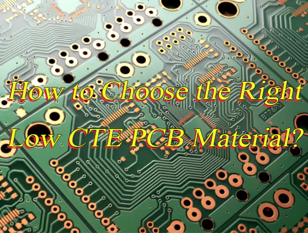
Why choose low CTE PCB material? Let’s discover types, selection guide, benefits, applications, cost for low CTE PCB material.
Are you troubled with these problems?
- How to solve high maintenance costs caused by solder joint cracking under high temperatures?
- How to reduce customer complaints about signal loss in 5G/800G high-frequency modules?
- How to overcome long lead times and high costs of imported materials in global supply chains?
As a low CTE PCB material supplier, EBest Circuit (Best Technology) can provide you service and solutions:
- Precise CTE Matching: Offer gradient materials (2.7-3.4ppm/°C) to eliminate thermal stress, extending solder joint life by 40% without premium pricing.
- High-Frequency Performance Optimization: Low Df (≤0.002) + stable Dk (≈4.7) materials reduce 10GHz signal loss by 35%, ensuring stable performance for 5G/data centers.
- Global Supply Chain Agility: Shorten lead times to 6-8 weeks with cost savings of 20% compared to imports, supporting flexible small-batch trials and rapid mass production.
Welcome to contact us if you have any request for low CTE PCB material: sales@bestpcbs.com.
What is Low CTE PCB Material?
Low CTE PCB material (low coefficient of thermal expansion printed circuit board substrate) is a type of substrate constructed by combining special reinforcement materials (such as low-expansion glass fiber cloth or quartz fiber cloth) with modified resins (polymers such as BT and PPO). Its core characteristic is a significantly lower coefficient of thermal expansion (CTE) than conventional FR-4 substrate (typically ≤5 ppm/°C).
This material is designed to match the thermal expansion characteristics of semiconductor chips (silicon CTE ≈ 2.5–3 ppm/°C), preventing delamination, warping, or solder joint fracture caused by significant CTE differences between the substrate and chip during temperature fluctuations. It is primarily used in applications with stringent thermal reliability requirements, such as high-density integrated circuit packaging, AI accelerator cards, and 5G communication equipment.
Common Low CTE PCB Materials Types
Glass Fabric-Based Low CTE Materials
- Classification: Composed of low-expansion fiberglass cloth (e.g., 1080, 2116, 7628 types) and modified epoxy/BT/PPO resins, CTE ≤5 ppm/°C, high-temperature resistance (Tg ≥170°C), thermal decomposition temperature Td ≥340°C.
- Features: Z-axis CTE ≤60 ppm/°C below Tg, ≤300 ppm/°C above Tg, matches silicon chip CTE (2.5–3 ppm/°C), reduces via crack risk.
- Advantages: 40% lower Z-axis expansion during high-Tg board soldering, 15% improved interlayer alignment accuracy for 20+ layer HDI boards, compatible with lead-free processes (T260 ≥30 min).
- Applications: High-density IC packaging, 5G communication equipment, consumer electronics motherboards; server motherboards use Tg170°C materials, automotive electronics select Tg ≥180°C for -40°C–150°C environments.
Quartz Fabric-Reinforced Low CTE Substrates
- Classification: Quartz fabric reinforcement with cyanate ester/PTFE resins, CTE as low as 2–3 ppm/°C, high-temperature resistance (>300°C), low dielectric loss (Df ≤0.002).
- Features: Nano-porous structure reduces dielectric constant (ε ≤2.5), thermal conductivity up to 170 W/(m·K), excellent corrosion resistance.
- Advantages: Ultra-low thermal expansion for aerospace precision instruments, reduced signal attenuation in high-frequency RF modules, high-temperature corrosion resistance in automotive power systems.
- Applications: Aerospace high-frequency RF modules, automotive power systems, precision medical electronics; localized reinforcement (e.g., BT resin) in 5G base stations reduces solder joint stress concentration.
Composite-Based Low CTE Laminates
- Classification: Dual-layer reinforced structures (e.g., CEM-1/CEM-3), CTE controlled at 6–8 ppm/°C, balancing cost and performance with epoxy glass cloth/paper cores.
- Characteristics: Tg ≥150°C, Td ≥310°C, passes 500-hour 85°C/85%RH test, peel strength ≥1.4 N/cm.
- Advantages: 20–30% cost savings vs. premium materials, suitable for industrial controls, automotive electronics, mid-range consumer products; excellent CAF resistance.
- Applications: Industrial control devices, automotive electronics, mid-range consumer products; metal-core boards enhance LED driver module thermal management.
Metal-Core Low CTE Materials
- Classification: Aluminum/copper/molybdenum substrates with insulating dielectrics (e.g., AlN), CTE close to chips (2.5–3 ppm/°C), high thermal conductivity (>200 W/(m·K)).
- Features: Aluminum substrates offer 1–3 W/(m·K), AlN ceramic substrates reach 170 W/(m·K); thermal conductivity drives PCB heat dissipation efficiency.
- Advantages: Combines low thermal expansion with efficient heat dissipation, mechanical stress resistance; ideal for high-power devices (LED modules, power modules).
- Applications: Power modules, LED packaging, automotive power systems; via arrays under chips reduce thermal resistance by 40%.
Ceramic-Based Low CTE Substrates
- Classification: Al₂O₃/AlN/Si₃N₄ ceramics bonded to copper foil via direct bonding or adhesive lamination, CTE 4–6 ppm/°C, high-temperature resistance (>500°C).
- Features: Dielectric constant ε ≤9.9, low loss (Df ≤0.001), stable high-frequency signal transmission, corrosion resistance, long lifespan.
- Advantages: Stable high-frequency signal transmission, corrosion resistance, long lifespan; suitable for RF modules, automotive power systems, aerospace electronics.
- Applications: RF modules, automotive power systems, aerospace electronics; high-frequency materials (e.g., Rogers 4350B) in 5G base stations achieve T288 >30 min.
Flexible Low CTE Substrates
- Classification: Polyimide (PI) film with aramid fiber reinforcement, CTE ≤15 ppm/°C, bend resistance >10,000 cycles, Tg ≥300°C.
- Features: Balances flexibility and thermal stability; chemical resistance, high design freedom.
- Advantages: Suitable for wearables, flexible displays, automotive sensor harnesses; hybrid pressing balances cost and performance in flexible displays.
- Applications: Wearables, flexible displays, automotive sensor harnesses; localized reinforcement reduces solder joint stress in BGA packaging areas.
Specialty Resin Low CTE Materials
- Classification: Modified PPO/PTFE/CE resins with optimized molecular structures to reduce CTE; suitable for high-frequency high-speed circuits.
- Features: Dielectric constant ε ≤3.5, low loss (Df ≤0.002), high-temperature resistance (Tg ≥200°C), Td ≥400°C.
- Advantages: Low loss at high frequencies, chemical resistance, high design freedom; suitable for microwave communication, high-speed circuits, medical electronics.
- Applications: Microwave communication devices, high-speed circuits, medical electronics; PTFE-based substrates (e.g., Teflon) in 5G base stations achieve T288 >60 min.
How to Choose Low CTE PCB Material?
Below is a selection guide to low CTE PCB material:
1. Thermal-Mechanical Requirements for Application Scenarios
- Automotive electronics require extreme temperature tolerance from -40°C to 150°C, prioritizing high-Tg FR-4 (Tg ≥180°C) or metal substrates (e.g., aluminum/copper) with CTE ≤5ppm/°C to match silicon chips.
- 5G high-frequency modules demand Dk ≤3.5, Df ≤0.002, recommending Rogers 4350B (CTE ≤5ppm/°C) or quartz-fabric-reinforced substrates.
- Aerospace applications require high-temperature (>300°C) and corrosion resistance, favoring AlN ceramic substrates (CTE ≈4ppm/°C) or quartz-fiber composite materials.
2. CTE Matching Between Substrate and Components
- Silicon chips exhibit CTE of 2.5–3ppm/°C, requiring substrates with CTE ≤5ppm/°C (e.g., low-expansion fiberglass cloth) or metal-core boards (e.g., CMC, CTE ≈6ppm/°C).
- For BGA packaging, ceramic substrate CTE ≈7ppm/°C must differ by ≤3ppm/°C from plastic packaging to avoid solder joint fatigue; high-density packages use localized reinforcement (e.g., BT resin) to reduce stress concentration.
- Flexible circuits match substrate CTE with PI film (CTE ≈15ppm/°C), reducing overall CTE to ≤12ppm/°C via aramid fiber composites.
3. Stack-Up Design and Material Combination Optimization
- Symmetrical stack-up design with uniform copper thickness (e.g., 2oz rolled copper for power layers, 1oz electrolytic copper for signal layers) minimizes Z-axis warpage.
- Thin fiberglass cloth (e.g., 106/1080) combined with low-CTE prepregs achieves Z-axis CTE ≤7ppm/°C, suitable for AI accelerator multi-layer structures.
- Hybrid designs (e.g., fiberglass + quartz cloth) balance cost and performance, controlling CTE at 4–6ppm/°C for industrial control equipment.
4. Thermal Management and Conductivity Synergy
- High-power devices (e.g., LED modules) require metal substrates (aluminum/copper/molybdenum) with thermal conductivity >200W/(m·K) or AlN ceramic substrates (170W/(m·K)).
- ANSYS thermal simulation optimizes heat dissipation paths, reducing thermal resistance by 40% via thermal via arrays to prevent CTE mismatch-induced hotspots.
- Phase-change materials (e.g., graphene heat sinks) enhance thermal conduction, ensuring temperature uniformity ≤±5°C to reduce delamination risks from thermal stress.
5. Reliability Verification and Testing Standards
- Z-axis CTE measured via TMA per ASTM E831; temperature cycling (-40°C~125°C, 1000 cycles) assesses delamination risk; 85°C/85% RH testing for 500 hours evaluates insulation performance.
- BGA solder joints require ≤5% crack rate after 600 thermal cycles, monitored via X-ray non-destructive testing.
- Ceramic substrates pass cold-thermal shock testing (-55°C~125°C, 500 cycles) per MIL-STD-883 standards.
6. Cost-Performance Balancing Strategies
- Consumer electronics use standard FR-4 (Tg150°C, 20% cost reduction); industrial equipment needs high-Tg FR-4 (Tg ≥170°C, 15% cost increase); high-frequency scenarios prefer modified epoxy/ceramic fills (30–50% cost increase).
- Avoid over-engineering (e.g., 2.4GHz signals need no high-frequency substrates); balance cost/performance via material combinations (e.g., fiberglass + PTFE).
- Standardized materials (e.g., IPC-4101) reduce procurement costs while ensuring performance consistency.
7. Process Compatibility and Manufacturing Feasibility
- PTFE substrates require sodium-naphthalene treatment for adhesion; metal substrates consider CTE matching and thermal design; drilling parameters adapt to material hardness (e.g., high-speed low-feed for ceramics).
- Lamination temperature profiles ensure full resin curing (Td ≥340°C) to avoid under-cure delamination or over-cure brittleness.
- Automated lines (laser drilling, plasma cleaning) enhance precision and reduce human error.
8. Standardized Testing and Supplier Collaboration
- CTE testing per IPC-TM-650 2.4.24 requires UL/ROHS compliance reports and batch data from suppliers.
- ANSYS thermal stress simulation and ADS signal integrity simulation optimize designs; joint prototyping (e.g., 10-panel tests) with substrate manufacturers ensures manufacturability.
- Long-term supplier partnerships ensure material stability and technical support, monitored via ISO 9001 audits.
Advantages of Low CTE PCB Material
- Enhanced Product Reliability, Reduced Failure Costs: Low CTE materials (2.7-3.4ppm/°C, matching silicon chips at 3ppm/°C) minimize solder joint fatigue and cracking from thermal cycling, lowering failure rates and reducing post-sale maintenance costs while improving product lifespan.
- Stable High-Frequency Signal Transmission: With low dielectric loss (Df ≤ 0.002) and stable dielectric constant (Dk ≈ 4.7), these materials ensure minimal signal loss in high-frequency scenarios (e.g., 5G, 800G switches), cutting 10GHz losses by up to 35% for precise signal integrity.
- Optimized Thermal Management, Extended Equipment Lifespan: Paired with high Tg (≥250°C), low CTE reduces via fracture risks in high-heat environments (e.g., AI servers, data centers), enhancing heat dissipation to lower operating temperatures and extend device reliability.
- Lower Supply Chain Risks & Procurement Costs: Domestic low CTE fiberglass (CTE=3.4ppm/°C) is 20% cheaper than imports, with integrated local production cutting costs by 15%. Shorter lead times (6-8 weeks vs. 16-20 weeks) ease supply chain pressures, reducing procurement expenses for AI hardware.
- Reduced Hidden Quality Losses, Enhanced Brand Value: Minimized thermal mismatch issues (e.g., delamination) cut external costs (customer churn, acquisition expenses), boosting retention by 15% and strengthening brand reputation for long-term competitiveness.
- Enabling Miniaturization & High-Density Design: Isotropic low CTE materials (e.g., TLX series) with balanced X/Y/Z-axis expansion allow 3D high-frequency circuit processing. Low Z-axis CTE (e.g., 7ppm/°C) supports compact millimeter-wave antenna integration (e.g., 128 units in 25mm²), meeting AI/communication miniaturization needs.
Applications of Low CTE PCB Materials
- High-Density Integrated Circuit Packaging (e.g., CPU/GPU Packages)
- AI Accelerator Cards & High-Performance Computing Modules
- 5G Base Stations & Millimeter-Wave Antenna Modules
- Automotive Electronic Control Units (ECU) & Power Modules
- Aerospace Electronics & Satellite Communication Systems
- Industrial Control Equipment & Automation Systems
- Medical Electronic Devices (e.g., Ultrasound/CT Machines)
- Consumer Electronics Motherboards (e.g., Smartphones/Tablets)
- LED Lighting & Display Module Packaging
- RFID & Microwave Circuits
- Flexible Display Modules & Wearable Devices
- Electric Vehicle Battery Management Systems (BMS)
- High-Speed Digital Circuits & Server Motherboards
- Precision Instruments & Sensor Modules
- Backplanes & Connectors in Communication Equipment
Difference Between Low CTE PCB and High CTE PCB Material
Thermal Expansion Coefficient Differences
- Low CTE: CTE ≤5 ppm/°C (e.g., 1080-type fiberglass cloth substrate), thermal expansion ≤12 μm/m in -55°C~125°C range, matches silicon chip CTE (2.5-3 ppm/°C). Example: Intel 14nm chip packaging uses low CTE material to improve solder joint thermal fatigue life by 30%, reducing delamination and solder fracture risks.
- High CTE: CTE ≥15 ppm/°C (e.g., standard FR-4 substrate), thermal expansion ≥30 μm/m in same range, causing interfacial stress concentration. Consumer electronics low-end motherboards often see 15% higher repair rates due to high CTE materials, with BGA solder joints prone to fatigue cracks and interlayer delamination.
Application Scenario Suitability
- Low CTE: Suitable for high-precision scenarios: 5G high-frequency modules (e.g., Huawei 5G base station uses Rogers 4350B with CTE ≤5 ppm/°C, reducing signal loss by 20%), aerospace RF modules (NASA Mars rover uses AlN ceramic substrate passing 300°C thermal shock test), automotive power systems (Tesla Model 3 BMS uses high-Tg FR-4 passing -40°C~150°C 1000-cycle test), medical imaging devices (Siemens CT scanner uses quartz fabric substrate for image stability improvement).
- High CTE: Suitable for low-cost scenarios: consumer electronics low-end motherboards (e.g., Xiaomi entry-level phone uses standard FR-4, reducing cost by 20%), industrial control non-precision circuits (PLC uses CEM-3 substrate for basic functionality), LED lighting substrates (streetlight driver boards use high CTE materials passing 85°C/85% RH 500-hour test).
Thermal Management Performance
- Low CTE: High thermal conductivity (>200 W/(m·K)) metal/ceramic substrates (e.g., aluminum substrate 2 W/(m·K), AlN ceramic 170 W/(m·K)), with 100μm via arrays reducing thermal resistance by 40%, avoiding local hotspots causing CTE mismatch. Example: Nvidia AI accelerator card uses metal substrate to improve heat dissipation efficiency by 30%.
- High CTE: Low thermal conductivity (<1 W/(m·K)) organic substrates (e.g., standard FR-4 0.3 W/(m·K)), requiring additional heat sinks or fans for auxiliary cooling, increasing design complexity. Low-end LED driver boards need added heat sinks to pass thermal tests.
Manufacturing Process Requirements
- Low CTE: Requires precision lamination control (Tg ≥170°C, Td ≥340°C), laser drilling (e.g., 50μm via accuracy ±2μm), plasma cleaning for adhesion enhancement. Example: Apple A-series chip packaging uses laser drilling to improve yield by 15%.
- High CTE: Standard FR-4 process suffices (Tg 130°C, Td 300°C), drilling parameters adapt to standard substrate hardness (e.g., 15000rpm for 3mm board thickness), reducing cost by 20-30%. Consumer electronics motherboards use standard process to improve production efficiency by 20%.
Reliability Verification Standards
- Low CTE: Requires ASTM E831 TMA for Z-axis CTE measurement, -40°C~125°C 1000-cycle test for delamination risk assessment, BGA solder joint 600-cycle thermal cycling crack rate ≤5% (X-ray inspection), ceramic substrates pass MIL-STD-883 thermal shock test (-55°C~125°C 500 cycles).
- High CTE: Meets JEDEC standard for -40°C~85°C 500-cycle no severe degradation, consumer electronics standards allow controlled delamination/solder cracks. Low-end motherboards pass 500-cycle test for market compliance.
Cost and Performance Balance
- Low CTE: Material cost 30-50% higher (e.g., Rogers 4350B is 3x standard FR-4 price), but reduces repair costs (e.g., automotive electronics repair rate drops from 15% to 5%), extends product lifecycle (medical devices from 5 to 10 years).
- High CTE: Material cost lower (standard FR-4 at 10 RMB/m²), suitable for cost-sensitive projects (e.g., consumer electronics entry-level products), but requires trade-offs in thermal-mechanical reliability (high CTE materials prone to delamination at high temperatures affecting stability).
Signal Integrity Impact
- Low CTE: Low dielectric loss (Df ≤0.002, e.g., PTFE substrate), stable high-frequency high-speed signal transmission, reduces signal attenuation (e.g., 5G base station signal loss decreases by 20%), with 50Ω±5% impedance control for signal integrity.
- High CTE: Higher dielectric loss (Df ≥0.01, e.g., standard FR-4), 10GHz signal attenuation increases by 30%, requiring additional shielding design (copper shield/absorbing materials), increasing design complexity and cost.
How Much Does Low CTE PCB Materials Cost?
| Material Type | Unit Price Range (USD/㎡) |
| Glass Fabric-Based Low CTE Materials | 40−100 |
| Quartz Fabric-Reinforced Low CTE Substrates | 150−300 |
| Composite-Based Low CTE Laminates | 80−180 |
| Metal-Core Low CTE Materials | 100−500 |
| Ceramic-Based Low CTE Substrates | 500−2,000 |
| Flexible Low CTE Substrates | 100−300 |
| Specialty Resin Low CTE Materials | 200−800 |
Why Choose EBest Circuit (Best Technology) as Low CTE PCB Material Supplier?
Reasons why choose us as low CTE PCB material supplier:
- Customized CTE Gradient Material Matching: Gradient low CTE materials (2.7-3.4ppm/°C) precisely match chip-to-substrate thermal expansion coefficients, reducing solder joint fatigue cracking and extending product life.
- High-Frequency Signal Performance Optimization Package: Low Df (≤0.002) + stable Dk (≈4.7) material combinations reduce 10GHz signal loss by 35% in 5G/800G modules, enhancing transmission stability.
- Global Supply Chain Rapid Response: 6-8 week lead times cut waiting time by over 50% compared to imports, supporting agile small-batch trials and mass production for international AI hardware clients.
- Cost Optimization Solutions: 20% cost reduction via integrated domestic “fiber-to-fabric” production, avoiding import premiums and boosting project cost competitiveness.
- Thermal Management Co-Design Support: Combining high Tg (≥250°C) and low CTE properties, providing thermal stress simulation and heat dissipation optimization for AI servers/data centers.
- Multi-Scenario Material Adaptation Library: Full-spectrum material library for consumer electronics to industrial devices, enabling rapid selection and parameter validation to shorten R&D cycles.
- Eco-Compliance Solutions: RoHS/REACH-compliant and recyclable material options, helping clients meet global environmental regulations and enhance CSR reputation.
- Long-Term Strategic Partnership Support: Continuous technology iteration and capacity assurance, building stable, trust-based long-term collaborations to adapt to market changes.
Welcome to contact us if you need any help for low CTE PCB material: sales@bestpcbs.com.