

Would you like to get a good LED lamp PCB solution? Let’s learn more about LED Lamp PCB’s application, heat dissipation solution, efficiency optimization, manufacturer selection, durability testing, and distinctions from LED bar PCBs.
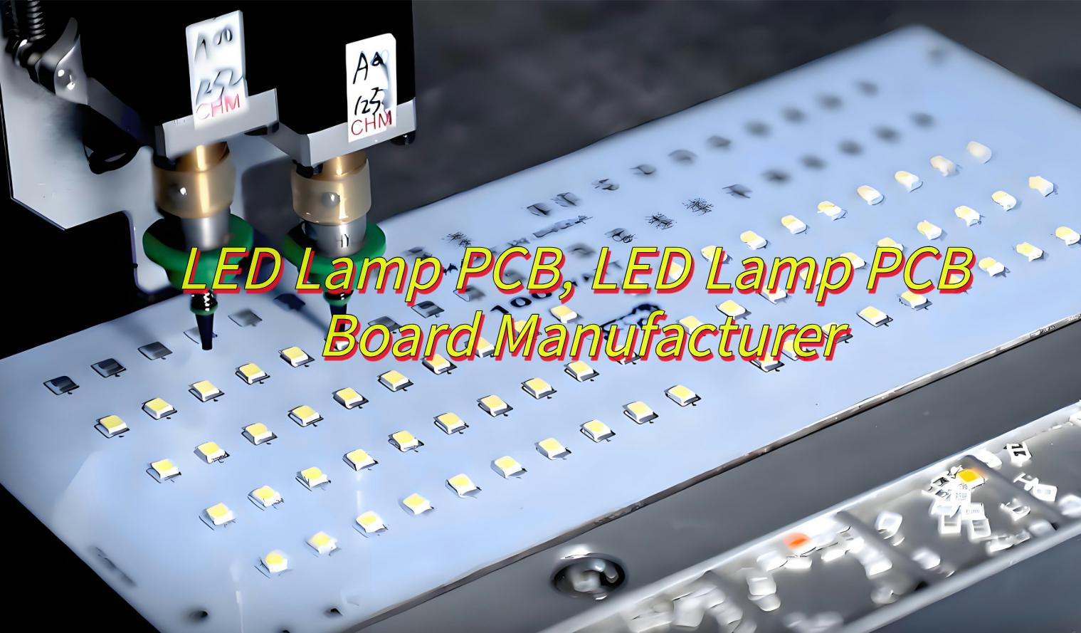
EBest Circuit (Best Technology) stands out as a leading LED lamp PCB manufacturer with diverse product options, rapid delivery, small-batch flexibility, and superior quality. Offering 50+ configurations (aluminum-core, FR4, hybrid), they deliver tailored solutions for streetlights, industrial systems, and smart lighting. Their streamlined production ensures a 7 days prototype turnaround and 15-25 days bulk order fulfillment, supported by our stable electronic supply chain and full automatic SMT production lines. Small orders (starting at 10 units) with no MOQ cater to startups. Rigorous testing (thermal cycling, ESD, AOI) ensures IPC-A-610 compliance. Trust EBest Circuit (Best Technology) for scalable, high-performance PCBs built for precision and reliability. Contact us today: sales@bestpcbs.com
What Is LED Lamp PCB?
An LED Lamp PCB (Printed Circuit Board) is a specialized circuit board designed to support and electrically connect Light Emitting Diode (LED) components in lighting applications. It serves as the foundation for LED lamps, enabling the integration of LED chips, drivers, resistors, capacitors, and other electronic components into a functional lighting system.
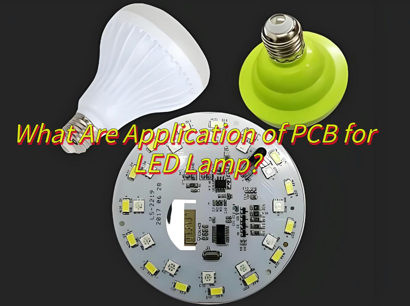
What Are Application of PCB for LED Lamp?
Here are application of LED Lamp PCB:
- General Lighting: Residential, commercial, and industrial lighting fixtures.
- Automotive Lighting: Headlights, taillights, and interior lighting.
- Signage and Displays: Backlighting for signs, billboards, and digital displays.
- Architectural Lighting: Custom lighting designs for buildings and landmarks.
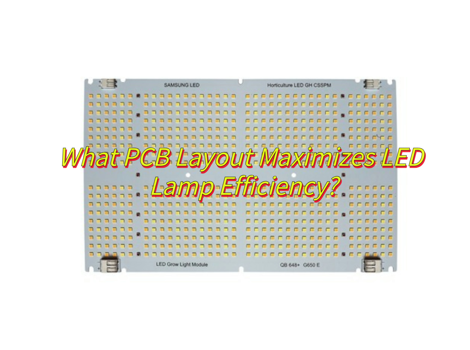
What PCB Layout Maximizes LED Lamp Efficiency?
Below are the critical factors and techniques to achieve maximizes LED lamp PCB efficiency:
Thermal Management
- Metal Core PCB (MCPCB): Use aluminum or copper substrates for superior heat conduction. These materials efficiently transfer heat away from LEDs, preventing overheating and reducing light degradation.
- Thermal Vias: Incorporate multiple thermal vias beneath LEDs to connect the top layer (with components) to inner or bottom layers, enhancing heat dissipation.
- Component Spacing: Maintain adequate spacing between high-power LEDs and heat-sensitive components (e.g., drivers, capacitors) to avoid thermal interference.
- Copper Pour: Add copper pours or polygons beneath LEDs to act as heat sinks, increasing the surface area for heat transfer.
Electrical Performance
- Short and Wide Traces: Use short, wide copper traces for power and ground connections to minimize resistance and inductance, reducing voltage drops and improving current delivery.
- Separate Power and Signal Layers: In multi-layer PCBs, dedicate specific layers for power and ground to isolate them from signal traces, minimizing noise and interference.
- Decoupling Capacitors: Place decoupling capacitors close to LED drivers and power supply pins to filter high-frequency noise and stabilize voltage.
- Avoid Sharp Bends: Use 45° or rounded trace corners instead of 90° bends to reduce impedance discontinuities and signal reflections.
Component Placement
- LED Arrangement: Group LEDs logically to minimize trace lengths and balance current distribution. Avoid long, serpentine traces that can cause voltage drops.
- Driver Proximity: Position LED drivers close to LEDs to reduce trace lengths and improve current regulation accuracy.
- Isolation of High-Power Components: Keep high-power components (e.g., MOSFETs, inductors) away from low-power signal traces to prevent electromagnetic interference (EMI).
- Test Points: Include test points at critical nodes (e.g., LED connections, driver outputs) for easy troubleshooting and performance verification.
Advanced Layout Techniques
- Ground Plane: Implement a solid ground plane on a dedicated layer to provide a low-impedance return path for current, reducing noise and improving signal integrity.
- Differential Pair Routing: For high-speed digital signals (e.g., LED control signals), route differential pairs with matched trace lengths and spacing to minimize skew and crosstalk.
- Stitching Vias: Use stitching vias around sensitive areas (e.g., analog circuits) to isolate them from noisy digital sections, improving signal isolation.
Simulation and Validation
- Thermal Simulation: Use thermal simulation tools (e.g., ANSYS, SolidWorks) to predict temperature distributions and optimize heat sink designs.
- Signal Integrity Analysis: Perform signal integrity simulations to identify and correct impedance mismatches, crosstalk, and reflections before fabrication.
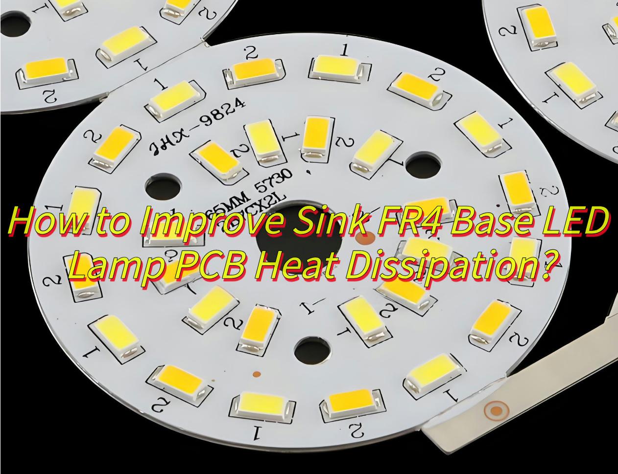
How to Improve Sink FR4 Base LED Lamp PCB Heat Dissipation?
To enhance heat dissipation in FR4-based LED lamp PCBs, implement these practical strategies:
- Increase Copper Thickness-Use thicker copper layers (≥2 oz) for power traces and ground planes to improve thermal conductivity.
- Optimize Thermal Vias-Add densely packed thermal vias under high-power LEDs to transfer heat to backside copper layers or heatsinks. Fill vias with conductive epoxy for better thermal bridging.
- Component Layout-Space out high-power LEDs to prevent localized heat buildup. Avoid placing heat-sensitive components (e.g., drivers) near hotspots.
- External Heatsinks-Attach aluminum/copper heatsinks to the PCB’s underside using thermal adhesive or screws. Ensure flat contact surfaces for optimal heat transfer.
- Thermal Interface Materials (TIMs)-Apply thermal pads, pastes, or phase-change materials between the PCB and heatsink to minimize interfacial thermal resistance.
- LED Selection-Choose LEDs with low thermal resistance (e.g., flip-chip or COB designs) to reduce junction-to-PCB heat transfer bottlenecks.
- Hybrid Substrates-Integrate localized metal-core (e.g., aluminum) or ceramic inserts under high-power LEDs while retaining FR4 for cost-effective areas.
- Active Cooling-For high-density designs, add low-profile fans or Peltier coolers to force airflow across the PCB surface.
- Current Management-Use constant-current drivers and derate LED operating currents (e.g., 80% of max rating) to lower heat generation without sacrificing brightness.
- Simulation & Testing-Perform thermal modeling (e.g., ANSYS) during design. Validate with IR thermography and monitor LED junction temperatures (<85°C).
How to Select A LED Lamp PCB Board Manufacturer?
To select a LED Lamp PCB Board Manufacturer for LED lamp production, prioritize these criteria with supporting references:
- Verify quality certifications (e.g., ISO 9001, UL, RoHS) and request third-party audit reports to ensure compliance with safety and environmental standards.
- Assess manufacturing capabilities: Confirm expertise in aluminum substrates, hybrid designs (FR4 + metal cores), and high-current trace layouts for thermal management.
- Evaluate material quality: Insist on military-grade laminates and high-temperature solder masks to prevent delamination under prolonged heat.
- Review industry experience:Prioritize manufacturers with proven LED lighting projects (e.g., stage lighting, industrial fixtures) and request case studies.
- Demand technical support: Ensure DFM (Design for Manufacturing) analysis, thermal simulation tools, and rapid prototyping services.
- Confirm testing protocols: Require AOI (Automated Optical Inspection), X-ray testing, and thermal cycling reports to validate reliability.
- Analyze cost structure: Compare quotes including tooling fees, bulk discounts, and hidden charges (e.g., IC programming, custom finishes).
- Verify logistics and scalability: Check lead times for small batches (≤72 hours) and capacity for large orders (≥10k units/month).
How Do Manufacturers Test LED Lamp PCB Durability?
LED Lamp PCB Manufacturers validate LED lamp PCB durability through these tests:
Temperature Cycling
- Expose PCBs to rapid temperature shifts (e.g., -15°C to 60°C) for 250 cycles to test thermal expansion resistance.
- Verify no cracking, delamination, or solder joint failures post-test.
Humidity Exposure
- Operate PCBs at 45°C with 95% humidity for 48+ hours to assess moisture resistance and insulation degradation.
- Check for corrosion, short circuits, or material warping.
Vibration Testing
- Apply 300 RPM vibrations at 2.54cm amplitude in X/Y/Z axes for 30 minutes each to simulate transportation stress.
- Confirm no component detachment or trace fractures.
Electrical Stress
- Run PCBs at 1.2x rated voltage/current for 24+ hours to detect overheating or power regulation failures.
- Monitor insulation resistance (>100MΩ) and dielectric strength (withstand 2x operating voltage).
Accelerated Lifespan Testing
- Continuously operate LEDs until light output drops to 70% of initial levels (typically 5,000–10,000 hours).
- Track thermal resistance (θ<sub>ja</sub>) to ensure <85°C junction temperatures.
Material Reliability Checks
- Perform ESD tests (HBM >2kV, MM >1kV) to validate anti-static protection.
- Expose to salt spray/acidic gas environments for 48+ hours to test corrosion resistance.
Switch Endurance
- Cycle power on/off (e.g., 20s ON / 20s OFF) for 10,000+ iterations to assess contact reliability.
What Are Differences Between LED Lamp PCB& LED Bar PCB?
Base Material:
- LED Lamp PCBs use aluminum substrates (copper + dielectric + metal core) for high-power thermal management.
- LED Bar PCBs use FPC (flexible) or rigid FR4 boards, depending on bendability needs.
Structure:
- Lamp PCBs feature multi-layer designs (e.g., 1oz–10oz copper) with dielectric insulation.
- Bar PCBs are single/double-layer with 0.1–0.3mm thickness for flexibility or rigidity.
Component Density:
- Lamp PCBs support high-density SMD components (e.g., COB LEDs) for focused illumination.
- Bar PCBs use spaced LEDs (e.g., 18–30 LEDs/30cm) for uniform linear lighting.
Applications:
- Lamp PCBs: High-power fixtures (streetlights, industrial lamps) requiring >10W output.
- Bar PCBs: Decorative/ambient lighting (signage, furniture) with 12V/24V low-voltage operation.
Cost:
- Lamp PCBs cost 30–50% more due to aluminum substrates and complex layering.
- Bar PCBs use cheaper FR4/FPC materials, with flexible versions priced 20% higher than rigid.
FAQs of LED Lamp PCB Manufacturing
Q1: What are the advantages of using aluminum PCBs in LED lamp manufacturing?
A1: Aluminum PCBs are popular in LED lamp manufacturing due to their excellent thermal conductivity, which helps to dissipate heat more effectively, improving the performance and lifespan of the LEDs.
Q2: How does the PCB’s surface finish affect LED lamp performance?
A2: The surface finish of the PCB, such as HASL (Hot Air Solder Leveling) or ENIG (Electroless Nickel Immersion Gold), affects solderability, durability, and the overall electrical performance. A high-quality finish ensures reliable connections and minimizes the risk of component failure.
Q3: Can LED lamp PCBs be customized for different types of LED applications?
A3: Yes, LED lamp PCBs can be tailored to meet the specific requirements of various LED applications, including size, shape, current capacity, and thermal management needs. Custom designs help optimize performance based on the intended use.
Q4: What is the importance of testing and quality control in LED lamp PCB manufacturing?
A4: Testing and quality control are crucial in ensuring that LED lamp PCBs function correctly, meet safety standards, and have a long lifespan. This includes electrical testing, thermal testing, and visual inspections to catch defects before the final product is assembled.
Q5: How do environmental regulations impact the manufacturing of LED lamp PCBs?
A5: Environmental regulations, such as RoHS (Restriction of Hazardous Substances) and WEEE (Waste Electrical and Electronic Equipment), ensure that LED lamp PCBs are free from harmful substances like lead and mercury. These regulations influence material choices and manufacturing processes to reduce environmental impact.