

PCB layers are the physical and electrical building blocks of a printed circuit board. It is a layered structure made by stacking copper and insulating materials together. Each layer serves a clear purpose, such as carrying signals, distributing power, or providing a stable ground reference. The way these layers are arranged directly affects how the board performs.
What are layers on a PCB?
A PCB is not just a flat sheet. It is a carefully stacked structure. Each layer has a clear job. Together, these layers allow electricity to flow in a controlled way.
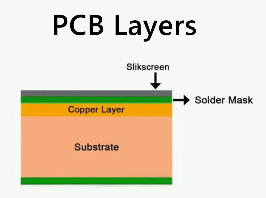
At the most basic level, a PCB layer can be copper, insulation, or surface coating. Copper layers carry signals and power. Insulation layers keep signals apart. Surface layers protect the board and make assembly possible.
PCB board layers define how complex a board can be. A simple product may need only two layers. A high-speed device may need many more. Each added layer increases routing space. It also improves signal control.
The layers of a PCB are planned during design. Engineers decide how many layers are needed. They also decide what each layer will do. This plan is called a PCB layer stackup.
Understanding PCB layers meaning helps avoid design mistakes. It also helps control cost. Too many layers waste money. Too few layers cause noise and routing problems.
At EBest Circuit (Best Technology), PCB layers design is part of our turnkey EMS service. From layout to final assembly, layer planning is handled early. This reduces risk and shortens lead time.
How are PCB layers produced?
PCB layers are produced through a precise and repeatable process. Each step matters. Small errors can affect the entire board.
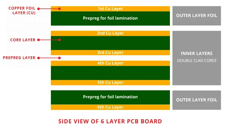
- The process starts with copper-clad laminate. This material has copper bonded to fiberglass. The fiberglass is usually FR-4. It offers strength and heat resistance.
- For inner layers, copper is first etched. A photo image defines the circuit pattern. Chemicals remove unwanted copper. What remains forms the traces.
- After etching, inner layers are inspected. Alignment is checked. Shorts and opens are detected early.
- Next comes lamination. Multiple etched layers are stacked together. Prepreg sheets are placed between them. Heat and pressure bond everything into one board.
- Once laminated, holes are drilled. These holes connect different PCB copper layers. Copper plating coats the hole walls. This creates electrical paths between layers.
- Outer layers are then formed. The same imaging and etching steps apply. Finally, solder mask and surface finish are added.
Throughout this process, PCB layers stack up accuracy is critical. Even slight shifts can cause failures. At EBest Circuit (Best Technology), automated inspection ensures layer alignment stays within tight limits. Because we control both PCB fabrication and assembly, feedback is fast. That is a key benefit of turnkey EMS services.
What does a 2 layer PCB mean?
A 2 layer PCB is the most common board type. It has copper on the top and bottom. Between them is an insulating core.
In a PCB 2 layers design, components usually sit on the top. Traces run on both sides. Vias connect the two copper layers. This structure is easy to understand. It is also cost-effective. That is why many consumer products use it.
However, routing space is limited. Power and signal traces share the same layers. This can cause noise in sensitive circuits. Still, for low-speed designs, a two-layer board works well. Simple power supplies often use this type. Basic controllers also fit well.
At EBest Circuit (Best Technology), we manufacture high-quality two-layer boards at scale. Even simple boards benefit from good material and process control.
What does a 4 layer PCB mean?
A 4 layer PCB adds two inner copper layers. This design offers more control and flexibility. It is common in modern electronics.
A typical 4 layers PCB stackup includes:
- Top signal layer
- Inner ground layer
- Inner power layer
- Bottom signal layer
This structure separates signals from power. It also reduces noise. Signals return through a solid ground plane. A PCB 4 layers design allows shorter traces. It improves impedance control. This matters for fast digital signals.
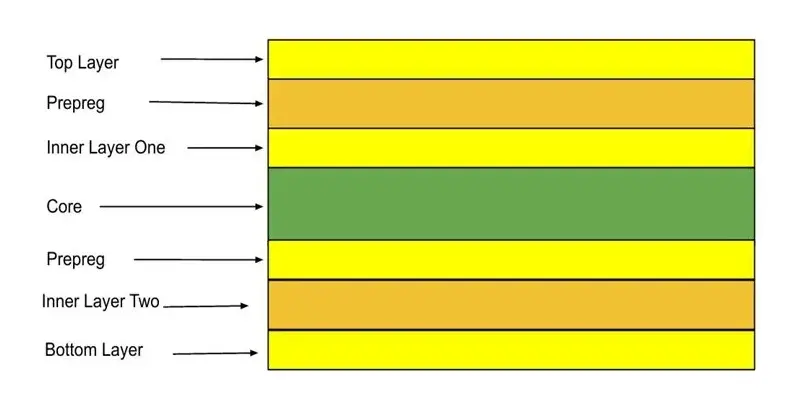
In a 4 layers PCB, routing becomes cleaner. Components have more placement freedom. EMI issues are easier to manage. Cost is higher than two layers. Performance is much better.
At EBest Circuit (Best Technology), four-layer boards are a common request. They fit well in industrial control and communication products.
Do PCB layers matter?
Yes, PCB layers matter a lot. They affect performance, reliability, and cost. More layers provide better signal integrity. They allow clean power distribution. They also reduce electromagnetic interference.
- Layer count affects thermal behavior. Inner planes help spread heat. This protects sensitive components.
- PCB layers also affect manufacturing yield. Complex stackups need tighter control. That is why experience matters.
Choosing the wrong number of layers can cause redesigns. Redesigns cost time and money. At EBest Circuit (Best Technology), engineers review layer decisions early. This avoids later issues. It is part of our turnkey EMS approach.
How to identify PCB layers?
Identifying PCB layers depends on tools and experience. There are several common methods.
- The simplest method is visual inspection. You can see top and bottom layers. Inner layers are hidden.
- X-ray inspection reveals internal structure. It shows copper planes and vias. This is common in quality labs.
- Another method is cross-section analysis. A small sample is cut and polished. Layers become visible under a microscope.
- Design files also tell the story. Gerber files define each layer. The PCB layers name is listed clearly.
At EBest Circuit (Best Technology), every board includes a clear stackup record. This supports traceability and quality control.
Why do PCBs have multiple layers?
PCBs have multiple layers to solve real problems. Modern electronics demand more from smaller spaces.
More layers mean more routing room. Traces do not have to cross. This simplifies layout. Multiple layers also improve signal quality. Ground planes provide stable reference paths. Power planes deliver clean voltage. They reduce ripple and noise.
High-density designs require many connections. Multiple layers make this possible without enlarging the board.
In advanced devices, safety also matters. Separate layers help isolate sensitive signals. PCB design layers work together as a system. Each layer supports the others.
How many layers can a PCB have?
The number of PCB layers varies widely. Two layers are common. Four layers are standard for many products.
High-end boards may have eight, twelve, or more layers. Some specialized designs go even higher. The PCB maximum layers depend on manufacturer capability. Material choice also matters.
The PCB with most layers is usually found in servers or networking equipment. These boards handle high-speed signals and power. More layers increase cost. They also increase build time. That is why layer count should match real needs.
At EBest Circuit (Best Technology), we can manufacture PCBs with up to 32 layers. This supports complex industrial and communication systems.
How to decide PCB layer?
Deciding PCB layer count starts with function. What does the product do? How fast are the signals?
- Power requirements come next. High current often needs dedicated planes.
- Size constraints matter. A smaller board often needs more layers.
- Cost targets guide decisions. Each extra layer adds expense.
- Reliability goals also influence the choice. Stable designs often use more layers.
At EBest Circuit (Best Technology), we assist during this stage. Our team reviews design goals. We suggest practical stackups.
Conclusion:
PCB layers define how a circuit board works inside. From simple two-layer boards to complex multi-layer designs, each layer has a purpose. Choosing the right PCB layers improves signal quality, reliability, and cost control.
For technical support or project inquiries, contact us at sales@bestpcbs.com