

What is high frequency inverter board? This guide covers its basics, how it works, function and application and differences from low-frequency ones through this blog.
Are you troubled with these questions?
- Is EMC interference crashing your inverter system?
- Does poor heat dissipation jack up costs and lower yields?
- Is supply chain chaos delaying deliveries?
As a professional PCBA service supplier, EBest Circuit (Best Technology) can provide you service and solution:
- DFM Design—Cut costs and boost yields upfront.
- Copper Block Cooling—Keep high-frequency operations stable.
- 1K+ Capacity & Agile Supply—On-time delivery, guaranteed.
Welcome to contact us if you have any inquiry for inverter board PCBA service: sales@bestpcbs.com.
What Is High Frequency Inverter Board?
A high-frequency inverter board is a power electronic device that converts direct current (DC) into alternating current (AC). Its core feature is the use of high-frequency switching technology (typically above 20kHz), which rapidly switches power devices (such as MOSFETs and IGBTs) on and off to achieve power conversion. Compared to traditional low-frequency inverters (50/60Hz), high-frequency inverter boards significantly reduce device size and improve efficiency by utilizing high-frequency transformers and pulse-width modulation (PWM) technology.
How Does a High Frequency Inverter PCB Board Work?
- DC input: DC power from batteries or solar panels enters the inverter board.
- High-frequency inversion: Power devices (such as IGBTs) switch rapidly under the control of high-frequency PWM signals, converting DC power into high-frequency AC pulses (typically 20kHz-1MHz).
- High-frequency transformation: High-frequency AC power is converted (stepped up or down) by a small high-frequency transformer.
- Rectification and filtering: The high-frequency AC power output from the transformer is converted to DC power by a rectifier bridge, and then smoothed to a stable DC voltage by a filter circuit.
- Power frequency inversion: The filtered DC power is converted to 50/60Hz AC power by an inverter circuit (such as a full-bridge or half-bridge configuration) and output to the load.
- Feedback control: A sampling circuit monitors the output voltage and current in real time and adjusts the PWM duty cycle to maintain a stable output.
What Does a High Frequency Inverter Board Do?
Functions of high frequency inverter PCB board:
- DC-AC Conversion: Converts DC power from batteries, solar panels, or other sources into 220V/50Hz or 110V/60Hz AC power for use in industrial equipment.
- Voltage/Frequency Regulation: Utilizing PWM control technology, the output voltage and frequency are adjustable to meet varying load requirements.
- Waveform Optimization: Utilizes sinusoidal or modified sine wave output to reduce harmonic interference and improve power quality.
- Protection Function: Integrated overvoltage, overcurrent, short-circuit, and overheating protection mechanisms ensure safe operation.
- Lightweight Design: The high-frequency transformer’s compact size reduces overall weight, making it easier to integrate and move.
What Is a High Frequency Inverter Circuit Board Used for?
Application of high frequency inverter circuit board:
- New Energy – Photovoltaic micro-inverters, energy storage converters.
- Industrial Automation – Servo drives, UPS (uninterruptible power supplies).
- Consumer Electronics – Automotive inverters, LED driver power supplies.
- Medical Equipment – Portable X-ray machines, laser therapy device power supplies.
Difference between Low Frequency and High Frequency Inverter Board
| Comparison Dimension | High-Frequency Inverter Board | Low-Frequency Inverter Board |
| Operating Frequency | >20kHz | 50/60Hz |
| Transformer Size | Small | Large |
| Efficiency | 90%-95% | 80%-90% |
| Size/Weight | Lightweight, 1/3-1/2 the volume of low-frequency models | Bulky, requires large installation space |
| Load Capacity | Light loads | Heavy loads |
| Impact Resistance | Weak | Strong |
| Noise Level | <30dB (quiet) | 40-50dB (noisy) |
| Cost | High initial cost, long-term energy savings | Low initial cost, high energy consumption |
| Lifespan | 5-8 years | 10-15 years |
| Application Scenarios | solar energy storage | industrial heavy-duty use |
Why Choose EBest Circuit (Best Technology) as Invert Board Assembly Manufacturer?
Reasons why choose us as high frequency invert board assembly manufacturer:
- High-Precision Automated Assembly – We use SMT for ±0.02mm placement accuracy, reducing manual errors by 90% and boosting first-pass yield to 99.8% to lower your repair costs.
- Flexible Modular Production – Switch from small batches (MOQ 50pcs) to mass production, converting prototypes to volume in 24-72 hours to speed up your product launch.
- Eco- friendly & Lead-Free Compliance – Fully RoHS/REACH-compliant with halogen-free solder and nitrogen reflow ovens, ensuring faster time to market.
- Dual X-Ray + AOI Inspection: Real-time checks on solder voids (<5%) and component polarity, covering 100% of hidden joints (BGA/QFN) to catch 95% of defects early.
- IP67 Protective Coating: Optional silicone/acrylic/polyurethane layers withstand -40°C~150°C, cutting salt/moisture/dust failures by 70% to extend outdoor product life.
- Extreme Stress Testing: 72-hour full-load testing under -20°C~85°C cycles ensures <0.1% field failure rates for rock-solid reliability.
- Component Traceability: QR codes track every supplier, date, and test result from wafer batch to assembly for instant failure analysis and quality control.
- Free DFM Optimization: Our free report suggests 20+ cost-saving design tweaks (e.g., pad spacing, layout) to cut your assembly expenses by an average of 15%.
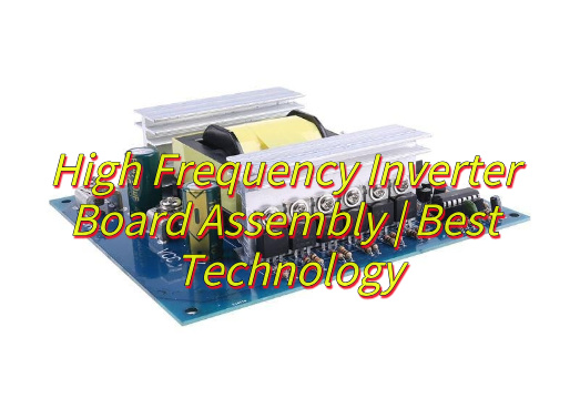
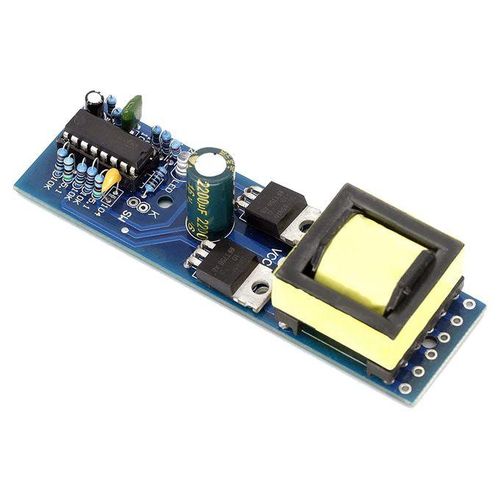
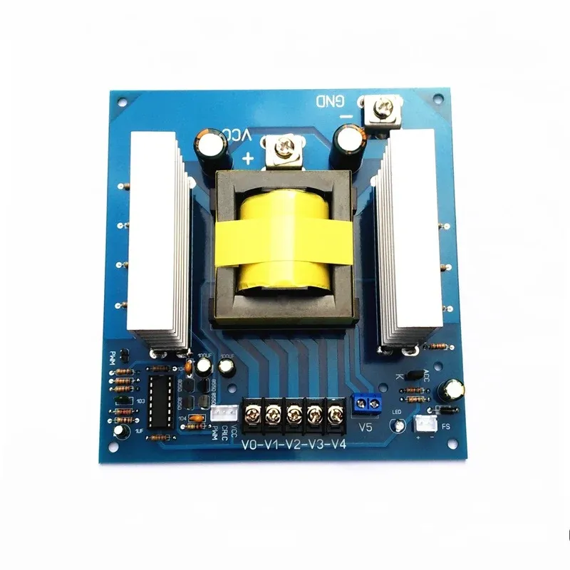
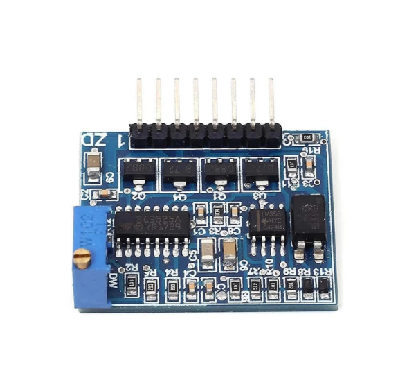
Below is a photo of inverter board we assembled:
Our PCB Assembly Capabilities
| Item | Capabilities |
| Placer Speed | 13,200,000 chips/day |
| Bare Board Size | 0.2 × 0.2 inches – 20 × 20 inches / 22 × 47.5 inches |
| Minimum SMD Component | 01005 |
| Minimum BGA Pitch | 0.25mm |
| Maximum Components | 50 × 150mm |
| Assembly Type | SMT, THT, Mixed assembly |
| Component Package | Reels, Cut Tape, Tube, Tray, Loose Parts |
| Lead Time | 1 – 5 days |
How to Get a Quote for Invert Board Assembly Service?
1. Core Design Documents
- PCB Production Files: Gerber files (including drill drawings); Impedance control requirements.
- BOM List: Full component list (model, package, manufacturer PN); Alternative part options clearly marked.
- Assembly Drawing: Component polarity markings; Heat sink mounting positions; Glue/potting points.
2. Process Specifications
- Soldering Method: Reflow / Wave / Selective soldering.
- Special Processes: Conformal coating areas; Potting thickness requirements; X-ray inspection points.
- ESD Protection: Compliance standard (e.g., ANSI/ESD S20.20).
3. Material Supply Options
- Customer-provided all materials.
- Assembler provides common parts (resistors/caps, etc.).
- Key component sourcing requirements (e.g., TI-authorized distributors).
4. Testing & Acceptance Criteria
- ICT/FCT Testing: Test program files (.pcf format)
- Burn-In Testing: Temperature cycle parameters (e.g., 85℃ full load, 4 hours)
- Visual Inspection: IPC-A-610 Class 2/3 standard
5. Order Basics
- Batch Quantity: Initial order + estimated monthly demand.
- Delivery Address (for logistics cost calculation).
- Packaging: ESD bags / Blister trays / Vacuum sealing.
Welcome to contact us if you have any request for high frequency inverter board assembly service: sales@bestpcbs.com.