

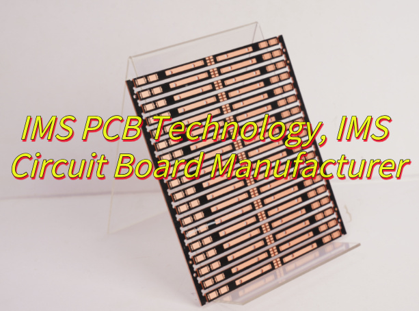
What is IMS PCB technology? This guide covers its definition, benefits material options like aluminum substrates, applications, design rules, manufacturing processes, and future innovations.
Are you bothered by these problems?
- Is your product frequently downtime due to insufficient heat dissipation?
- Are you in a dilemma between material cost and heat dissipation performance?
- Does space limitation limit your PCB design flexibility?
EBest Circuit (Best Technology) can provide:
- Our IMS PCB uses a high thermal conductivity aluminum substrate, which reduces thermal resistance by 50% to ensure continuous and stable operation.
- Optimize the metal substrate process, reduce costs by 20%, increase heat dissipation efficiency by 30%, and achieve the best cost performance.
- Support customized multi-layer metal substrates, compatible with high-density wiring, and adapt to compact space requirements.
Welcome to contact us if you have any request for IMS PCB: sales@bestpcbs.com.
What Is IMS PCB Technology?
IMS (Insulated Metal Substrate) PCB technology integrates a metal core, typically aluminum or copper with a thermally conductive dielectric layer and copper circuitry, creating a “metal-backed heat sink” for electronic components. Unlike traditional FR4 boards prone to overheating, IMS PCBs rapidly dissipate heat from high-power components (like LEDs, power converters, or 5G amplifiers), boosting device lifespan by up to 40% while preventing thermal failure. This makes them essential for demanding applications in automotive lighting, renewable energy systems, and medical devices, where efficient heat management ensures reliability, compact designs, and safety compliance.
What Are Advantages of IMS PCB Technology?
Benefits of IMS PCB Technology
- Superior Heat Dissipation – Aluminum cores efficiently transfer heat away from high-power components (e.g., LEDs, power modules), reducing thermal stress and extending lifespan. Ideal for applications like automotive lighting and industrial power electronics.
- Enhanced Durability – Metal substrates provide mechanical strength, resisting vibration and shock—critical for rugged environments (e.g., aerospace, automotive).
- Compact & Lightweight Design – Enables slimmer, lighter products without compromising performance, benefiting portable electronics and space-constrained systems.
- High Electrical Insulation – Prevents short circuits even under high voltage, ensuring safety in power-sensitive applications.
- Cost-Effective Longevity – Reduced cooling requirements (e.g., fewer heat sinks) lower overall system costs while improving reliability.
What Are Applications of IMS PCB Technology?
Applications of IMS PCB Technology
- LED Lighting: High-power LED systems (e.g., streetlights, headlights) for heat dissipation and durability.
- Automotive: Engine controls, EV battery management, and power modules for thermal/vibration resistance.
- Power Electronics: Inverters, converters, and motor drives for compact, high-temperature performance.
- Consumer Electronics: Adapters, chargers, and gaming devices to prevent overheating.
- Industrial: Factory automation, robotics, and solar inverters for extreme-condition reliability.
What Are Substrate Material Types of IMS PCB?
Aluminum (AL) Substrates
- Most common, cost-effective, and lightweight.
- Thermal conductivity: 1–4 W/m·K (standard) to 10–15 W/m·K (premium grades).
- Best for: LED lighting, power supplies, and automotive electronics.
Copper (Cu) Substrates
- Higher thermal conductivity (up to 400 W/m·K).
- More expensive but ideal for ultra-high-power applications (e.g., EV inverters, high-density power modules).
Steel Substrates
- Lower cost, but heavier and less thermally conductive (≈ 1–2 W/m·K).
- Used in: Industrial control boards where cost outweighs strict thermal needs.
Ceramic Substrates (Alumina, AlN, BeO, SiN)
- Ultra-high thermal conductivity (AlN: 80–200 W/m·K).
- Brittle and expensive, but critical for aerospace, high-frequency RF, and high-power electronics.
Composite Substrates (e.g., Al+FR4 Hybrid)
- Combines metal core with FR4 layers for mixed-signal designs.
- Balances cost and thermal management in complex PCBs.
Choosing the Right Substrate:
- For cost & general use: Aluminum.
- For extreme heat dissipation: Copper or ceramics.
- For rugged environments: Steel or hybrid composites.
IMS PCB Design Guidelines
Insulated Metal Substrate PCB Design Guidelines:
1. Material Selection
- Base Metal: Aluminum (1060, 5052, 6061) or copper, thickness 0.5–3.0 mm.
- Dielectric Layer: Epoxy resin with inorganic fillers (75–150 µm), thermal conductivity 8–12× FR4.
- Copper Foil: 1–5 oz (35–140 µm), surface finishes: HASL, ENIG, OSP..
2. Layer Stackup
- Single-Sided: Metal base → dielectric → copper circuit.
- Double-Sided Hybrid: FR4 core + thermal vias for heat dissipation.
- Multi-Layer: Metal-core layers interleaved with FR4 for complex routing.
- Thermal Vias: Array of vias (≥0.3 mm dia) to conduct heat to the metal base.
3. Thermal Management
- Thermal Resistance: IMS PCBs achieve 100× lower thermal resistance than FR4 (e.g., 0.15 mm dielectric vs. 1.6 mm FR4).
- Heat Dissipation: Prioritize component placement near the metal base; use thermal vias for high-power devices.
- Simulation: Validate thermal performance using ANSYS.
4. Electrical Performance
High-Speed Design:
- Use stripline for signals >15 Gbps; microstrip for <15 Gbps.
- Impedance control: 50Ω (single-ended), 100Ω (differential).
- Dielectric material: Rogers 4350B (Dk=3.48, Df=0.0037) for frequencies >5 GHz.
- Power Integrity: Dedicate power/ground layers; minimize via stubs in high-speed traces.
5. Manufacturing Considerations
Minimum Features:
- Line/space: 0.075 mm (1 oz Cu) to 0.275 mm (5 oz Cu).
- Drill size: Mechanical ≥0.3 mm, laser ≥0.1 mm.
- Tolerance: Layer thickness ±8%, line width/spacing ±20%.
- Surface Finish: ENIG for fine-pitch components; HASL for cost sensitivity.
6. Reliability & Testing
- Thermal Cycling: -40°C to 125°C, 1,000 cycles with <5% delamination.
- Insulation Resistance: >100 MΩ at 500V DC.
- Dielectric Withstanding: AC 1,000V/1 min no breakdown.
7. Application-Specific Tips
- LED Lighting: Place LEDs directly on the metal base; use thick copper (3–5 oz) for current paths.
- Automotive/Aerospace: Prioritize CTE matching between dielectric and metal base to avoid thermal stress.
8. Design Rules Summary
| Parameter | Recommendation |
| Dielectric Thickness | 75–150 µm |
| Copper Weight | 1–5 oz (35–140 µm) |
| Thermal Vias | Array density ≥10 vias/cm² |
| Minimum Trace/Space | 0.075 mm (1 oz Cu) |
| Impedance Control | ±10% tolerance |
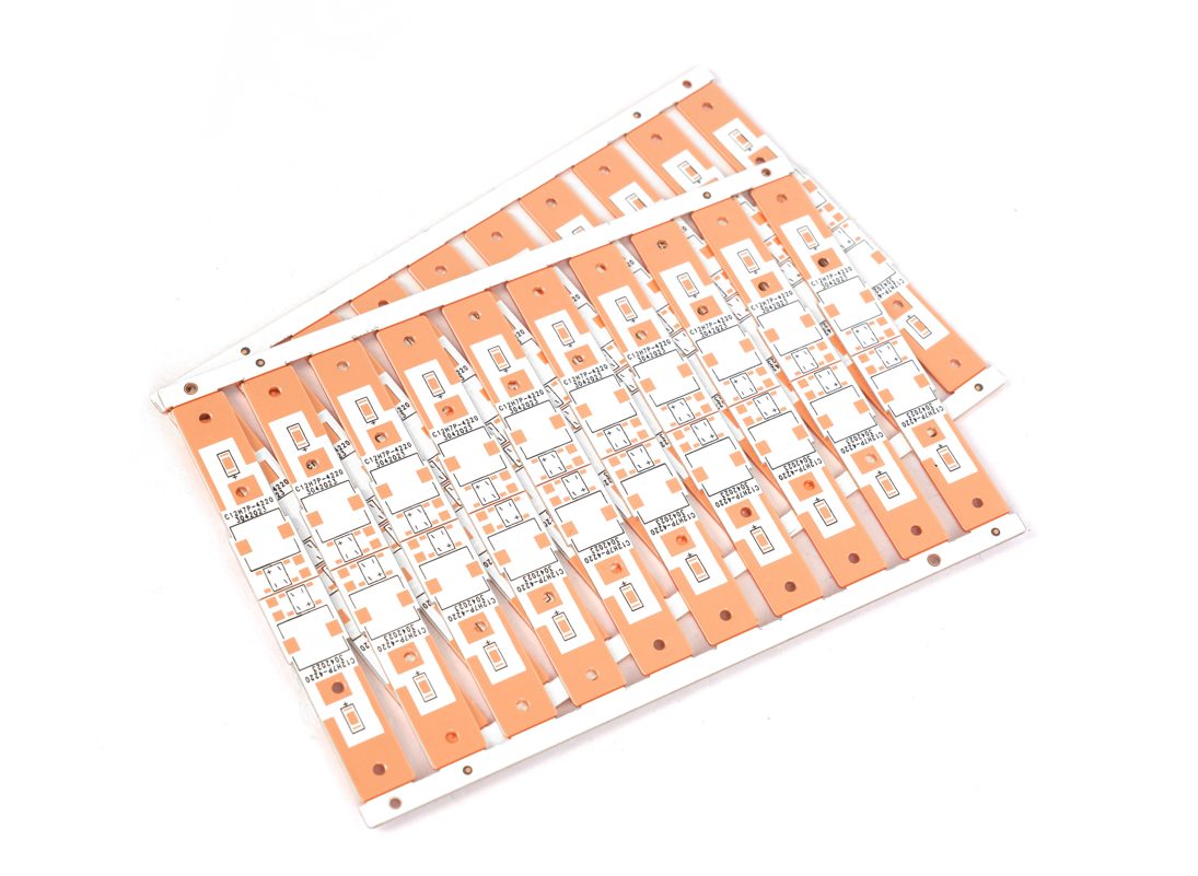
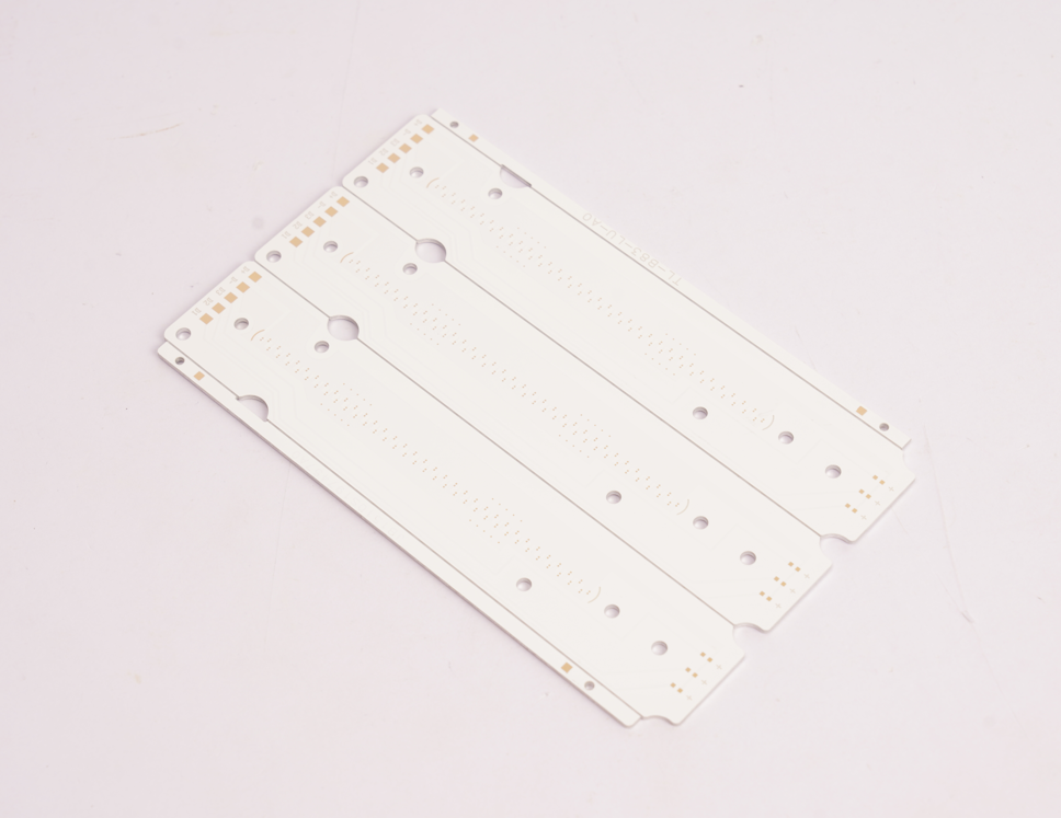
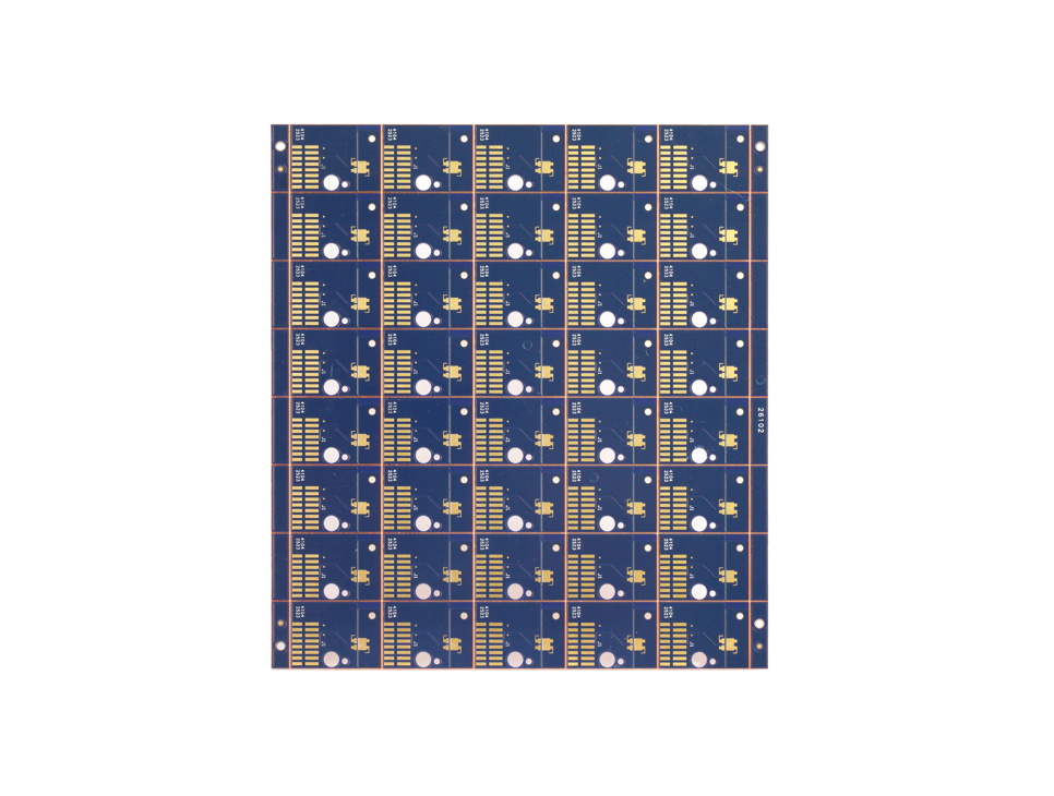
IMS Circuit Board Manufacturing Processes
IMS PCB Manufacturing Processes
1. Material Preparation
- Base Metal: Aluminum (1060, 5052, 6061) or copper sheets (0.5–3.0 mm thickness), pre-laminated with copper foil (1–5 oz).
- Dielectric Layer: Ceramic/boron-filled epoxy resin (75–150 µm), thermal conductivity 8–12× FR4.
- Pre-Treatment: Clean metal surface, apply photoresist, and expose to UV light for pattern hardening.
2. Layer Stackup & Imaging
- Lamination: Stack prepreg (epoxy-coated glass fiber), base material, and copper foil. Press at 150–200°C under 3–5 MPa.
- Outer Layer Imaging: Use transparent film masks and UV exposure to define copper traces. Develop unexposed areas with alkaline solutions.
3. Etching & Drilling
- Chemical Etching: Remove unprotected copper using ammonium persulfate or ferric chloride. Control etch time for inner layer precision.
- Precision Drilling: CNC-controlled drilling (≥0.1 mm diameter, 150,000 RPM). X-ray alignment for through-holes and microvias.
4. Plating & Surface Finish
- Electroless Copper: Deposit 1 µm copper on hole walls for interlayer conductivity.
- Electroplating: Thicken copper to target weight (e.g., 35 µm) and apply tin shielding.
- Surface Treatment: ENIG (electroless nickel/immersion gold), OSP (organic solderability preservative), or HASL (hot air solder leveling).
5. Thermal Management & Testing
- Thermal Cycling: -40°C to 125°C for 1,000 cycles. Insulation resistance >100 MΩ at 500V DC.
- Dielectric Testing: AC 1,000V/1 min without breakdown.
- AOI (Automated Optical Inspection): Verify trace/space accuracy (±20% tolerance) and defect detection.
6. Final Fabrication & QA
- CNC Routing: Shape boards with ±0.1 mm tolerance.
- Silkscreen: Print identifiers, warnings, and component labels.
- Packaging: Vacuum-seal with desiccant; include CoC (Certificate of Conformance) and material certs (e.g., UL 94V-0).
Why Choose EBest Circuit (Best Technology) as IMS Circuit Board Manufacturer?
Reasons why choose EBest Circuit (Best Technology) as IMS circuit board manufacturer:
- Proven Thermal Expertise – Engineered for high-power applications with optimized heat dissipation.
- Tight Tolerances (±0.05mm) – Precision manufacturing for demanding designs.
- Fast Turnaround (24 hours Prototype, 5-7 days Production) – Accelerated timelines without quality compromise.
- Turnkey Solutions – Full-service PCB manufacturing from design to delivery, accelerating your product’s time-to-market.
- ISO 14001/ISO 13485 certification: medical/automotive customers are exempt from secondary testing, and compliance costs are reduced by 30%
- Cost-Effective Solutions – Bulk discounts and material optimization reduce PCB costs.
- Hybrid PCB Capabilities – Seamless IMS-FR4 integration for complex layouts.
- ROHS/REACH Compliance – Eco-friendly materials for global market access.
- Custom Dielectric Formulations – Tailored thermal conductivity (1.5–5.0 W/m·K).
Welcome to contact us if you have any request for IMS PCB: sales@bestpcbs.com.
Future IMS PCB Technology Trends
Advanced Thermal Materials
- Use of high-thermal-conductivity ceramics (e.g., AlN, BeO) for extreme heat dissipation.
- Development of flexible IMS substrates with better thermal performance.
Miniaturization & High-Density Interconnects
- Microvias and HDI technology for compact designs in automotive/5G applications.
- Embedded components (resistors, capacitors) to reduce footprint.
Automotive & EV Focus
- High-power IMS PCBs for inverters, battery management, and motor drives.
- AEC-Q200 compliance for reliability in harsh environments.
Integration with AI & IoT
- Smart PCBs with embedded sensors for real-time thermal monitoring.
- AI-driven design optimization for thermal efficiency.
Sustainable Manufacturing
- Lead-free, halogen-free materials to meet RoHS/REACH standards.
- Recyclable metal cores (Al, Cu) for eco-friendly production.
High-Frequency & High-Speed Applications
- Low-Dk dielectric materials for 5G/mmWave RF applications.
- EMI shielding integration to minimize signal interference.
Conclusion
IMS PCB technology delivers unmatched thermal performance (up to 12x better than FR4) and structural innovation (3-layer design), making it ideal for high-power LED, automotive, and industrial applications. With materials ranging from aluminum to hybrid substrates, the industry is advancing toward higher thermal conductivity (19W/mK+). EBest Circuit (Best Technology) combines precision (±0.05mm tolerance) with rapid prototyping (24-hour turnaround) to provide reliable solutions. Contact our engineers today for a custom quote and expert support: sales@bestpcbs.com.