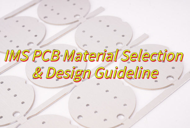
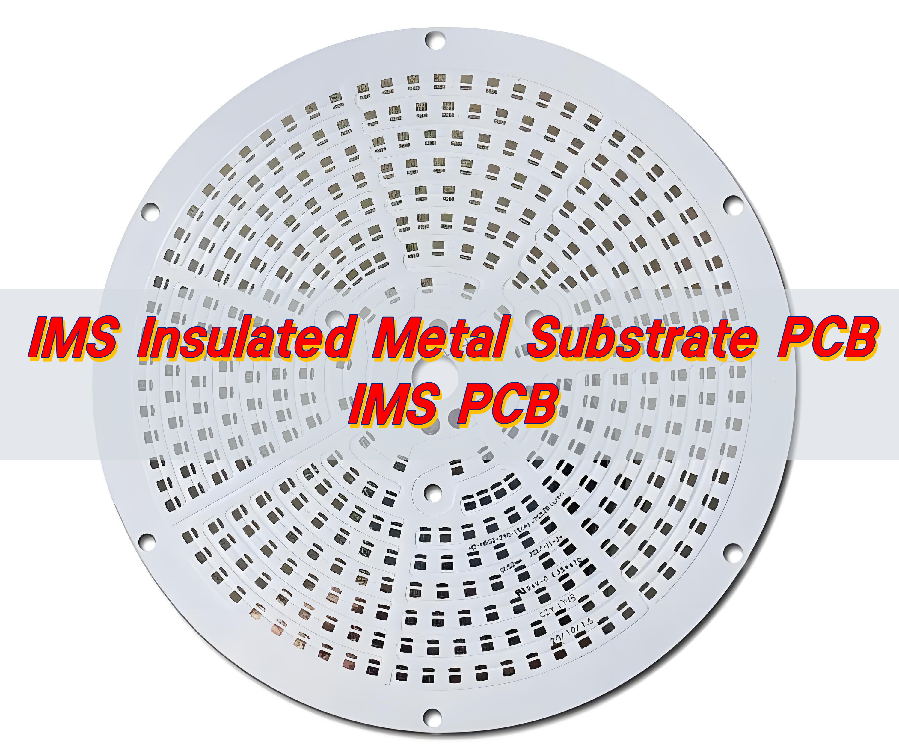
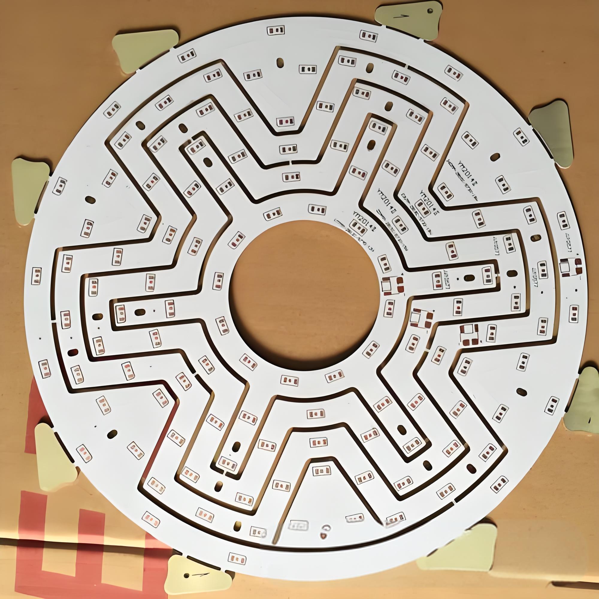
pcb
Home > Blog

Posts Tagged ‘IMS PCB material’

IMS Insulated Metal Substrate PCB, IMS PCB
Friday, July 25th, 2025

What is an IMS PCB?

Unlike traditional PCBs that rely on FR4 or other resin-based materials, IMS PCBs use a metal base—typically aluminum or copper. This base is paired with a dielectric layer and a copper circuit layer on top.

It’s not just a circuit board. It’s a thermal solution that keeps devices cool and running longer.

IMS Insulated Metal Substrate PCB, IMS PCB

IMS PCB full form and meaning?

The full form of IMS PCB is Insulated Metal Substrate Printed Circuit Board. It’s a PCB built to move heat away from components. That means better reliability, higher efficiency, and longer lifespan for your electronic products.

In this type of PCB, the metal substrate acts as a heat spreader. The insulation layer isolates the copper circuit from the metal base, while still allowing heat to pass through. It’s a smart design that balances performance with thermal control.

What is IMS material?

The core of every IMS PCB lies in its materials. These layers provide the best thermal and electrical performance. Here’s what you’ll find in a standard IMS stack:

  • Metal Base Layer: Usually aluminum for cost-efficiency and light weight. Copper is also used when more heat dissipation is required.
  • Dielectric Layer: A thermally conductive but electrically insulating material. It transfers heat from the circuit layer to the metal base.
  • Copper Circuit Layer: This is where the actual electrical routing happens. It’s similar to traditional PCB copper layers but optimized for thermal contact.

These three layers form the structure of IMS. The combination is compact, efficient, and powerful—especially in LED lighting, automotive electronics, and power converters.

The insulation layer, in particular, must handle high thermal loads while resisting electrical breakdown. Advanced IMS designs often use proprietary dielectric materials to increase thermal conductivity and reduce overall thickness.

How thick is a IMS PCB?

The thickness of an IMS PCB depends on the application. But typically, here’s what you can expect:

  • Metal base layer: 0.5mm to 3.2mm
  • Dielectric layer: 0.03mm to 0.2mm
  • Copper layer: 0.035mm to 0.2mm

The total thickness usually ranges from 0.8mm to 3.5mm. For LED lighting and compact modules, thinner IMS boards (like 1mm) are common. But in power-heavy designs, thicker boards provide the support and thermal capacity needed.

IMS Insulated Metal Substrate PCB, IMS PCB

Some custom builds even exceed 3.5mm if the heat demands are extreme. A thicker aluminum layer enhances mechanical strength and heat dissipation, but it also increases weight and cost. So choosing the right thickness is a balance of thermal needs and design efficiency.

What is the difference between FR4 and IMS PCB?

FR4 PCBs use glass-reinforced epoxy as their core. They are great for general electronics. But FR4 struggles with thermal stress. When high-power components run hot, FR4 doesn’t cool them fast enough. That leads to overheating and failure.

IMS PCBs, on the other hand, are built for thermal performance. The metal base acts like a built-in heat sink. It draws heat away from critical components and spreads it out. That protects the electronics and improves reliability.

FeatureFR4 PCBIMS PCB
Core MaterialEpoxy-based fiberglassMetal (usually aluminum)
Thermal Conductivity~0.25 W/mK1.0–9.0 W/mK or more
Heat DissipationLimitedExcellent
CostLowerSlightly higher, but worth it
Mechanical StrengthModerateStronger due to metal core

For everyday consumer electronics, FR4 is fine. But for power-hungry devices, IMS PCBs offer unmatched reliability.

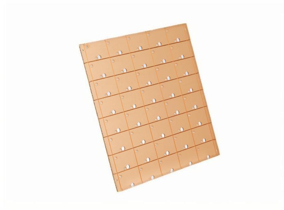
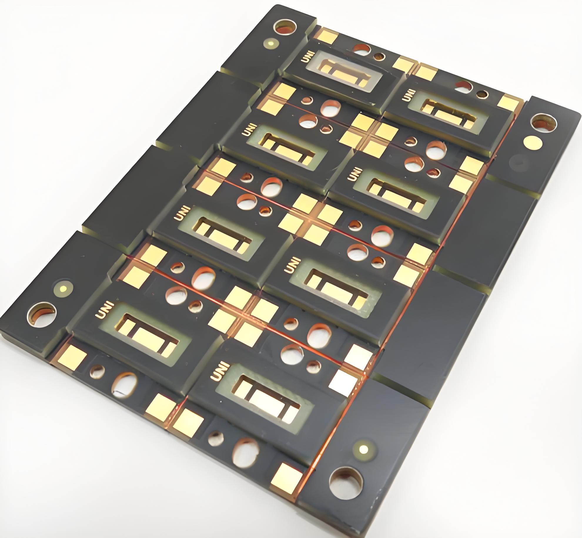
2 layer IMS PCB vs Multilayer IMS PCB

While single-layer IMS boards are most common, especially in LED lighting, 2-layer and multilayer IMS PCBs are gaining ground in complex applications.

2-layer IMS PCB means there are copper circuits on both sides of the dielectric layer, with one metal core layer. These offer more routing options while still allowing good heat dissipation.

Multilayer IMS PCBs, on the other hand, can include several copper layers, separated by insulation, and only one side is connected to the metal base for heat transfer. This allows for complex routing and high component density while keeping thermal control.

IMS Insulated Metal Substrate PCB, IMS PCB

Benefits of 2-layer IMS PCB:

  • Better circuit flexibility
  • Moderate thermal management
  • More design freedom

Benefits of Multilayer IMS PCB:

  • High circuit complexity
  • Suitable for dense power modules
  • Thermal performance still superior to FR4

If you’re building a simple LED module, a single or 2-layer IMS may be enough. But if you’re designing a power controller, communication device, or automotive ECU, multilayer IMS is often necessary.

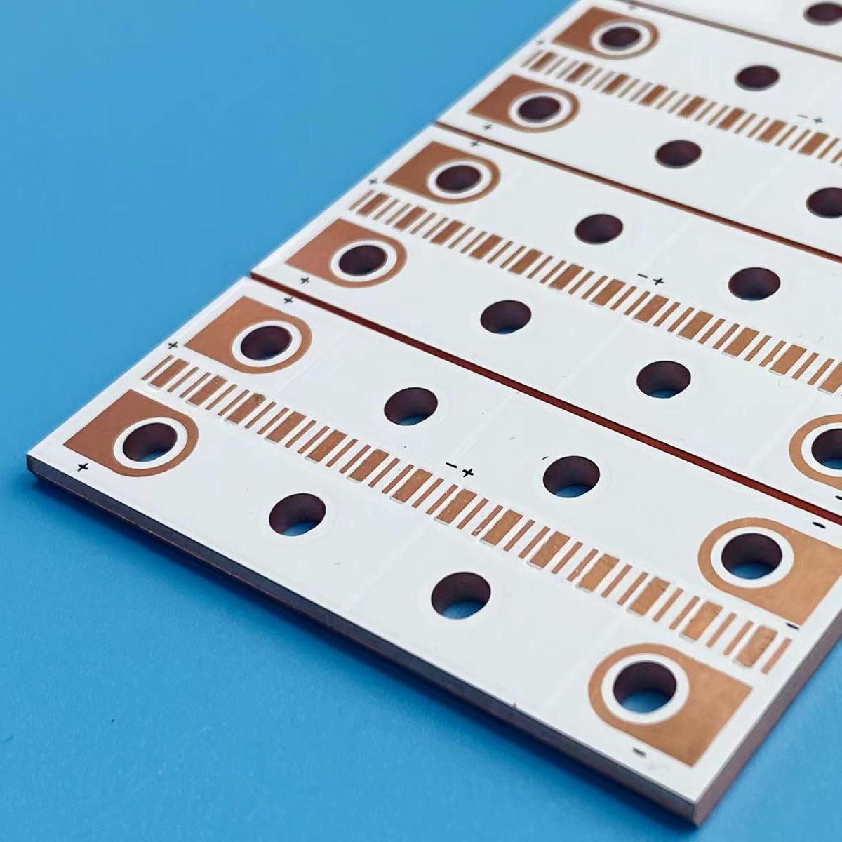
IMS PCB stackup: What to know?

Stackup design is more than just layers, it defines how your board handles heat, power, and performance. A typical IMS PCB stackup looks like this:

  • Copper circuit layer
  • Dielectric insulation layer
  • Metal substrate (usually aluminum)

But there’s room for customization. Here’s what matters:

  • Copper thickness: Choose 1oz, 2oz, or more depending on current flow.
  • Dielectric performance: The higher the thermal conductivity (measured in W/mK), the better the heat transfer.
  • Metal base: Aluminum is the go-to for most. But copper or stainless steel can be used for extreme performance or rigidity.
  • Surface finish: Choose between HASL, ENIG, OSP, or others based on your assembly process.

Stackup choices directly affect reliability. A poor choice here means components will overheat, solder joints will crack, or performance will drop.

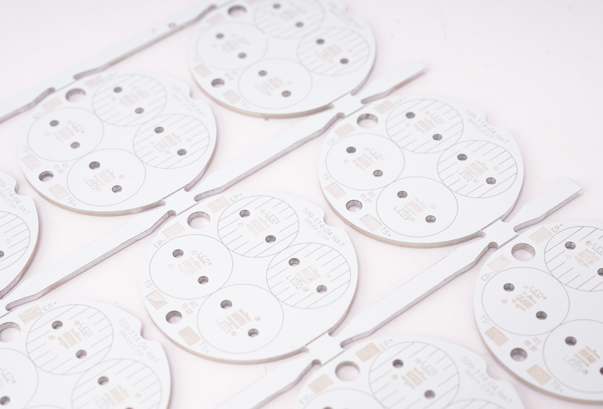
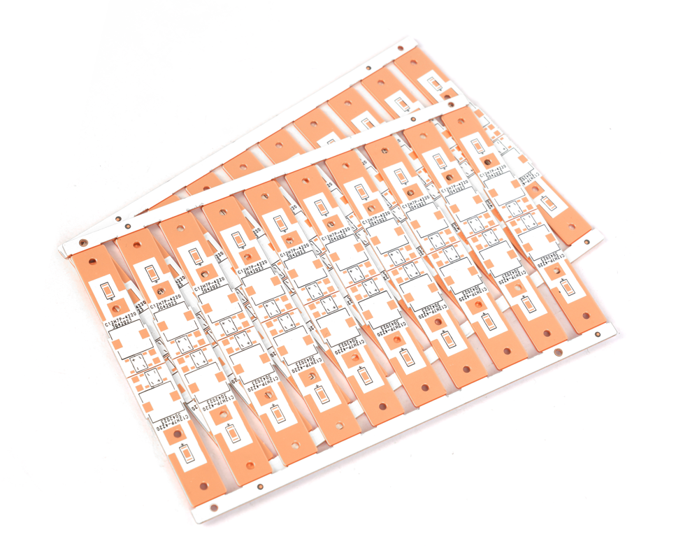
What are the applications of IMS PCB?

IMS PCB is widely used in high power industry.

  • LED lighting: Keeps high-brightness LEDs cool, extending their life.
  • Automotive electronics: Used in headlights, sensors, battery modules.
  • Power converters: Manages heat in inverters and converters.
  • Industrial control systems: Ensures smooth performance under high power loads.
  • Communication base stations: Maintains signal integrity and prevents thermal breakdown.

Why choose the right IMS PCB Manufacturer?

At Best Technology, we understand the critical role IMS PCBs play. We’ve spent years perfecting the production process, materials, and stackup customization. Every board we deliver is tested for:

IMS Insulated Metal Substrate PCB, IMS PCB
  • Thermal conductivity
  • Mechanical strength
  • Electrical reliability

Whether you need standard single-layer boards or complex multilayer IMS PCBs, we can build it to your exact needs.

Conclusion:

IMS PCB is very important in high power electronics. From simple LED lights to advanced power modules, IMS boards keep your devices cool, stable, and efficient.

Looking for an IMS PCB manufacturer you can rely on? Contact us today at sales@bestpcbs.com

IMS PCB Material Selection & Design Guideline
Tuesday, July 22nd, 2025

Are you worried about how to choose IMS PCB material for your project? Let’s explore its definition, properties, datasheet, types, IMS PCB material selection and design guidelines through this blog.

  • Wrong choice of substrate material leads to too high thermal resistance?
  • Is the dielectric layer easy to delaminate during multi-layer IMS design?
  • Is the dielectric loss too large under high-frequency application?

Best Technology Can Provide:

  • Provide 5 standardized thermal conductivity levels (1.5~8W/mK); Free sample matching tool, generate selection report in 30 minutes.
  • Patented resin system, peel strength>1.8N/mm; Support 3-layer lamination process, provide design specification manual.
  • Df value as low as 0.002 (@10GHz); Equipped with HFSS simulation model library, plug-and-play.

Welcome to contact us if you have any request for IMS PCB or MCPCB: sales@bestpcbs.com.

What Is IMS Material?

IMS material, known as insulated metal substrate, consists of a metal core, typically aluminum or copper, coated with a dielectric insulation layer and a conductive copper layer for circuit traces. This structure delivers outstanding thermal management, with aluminum-based versions achieving thermal conductivity of 1-3 W/(mĀ·K), while copper-based variants exceed 400 W/(mĀ·K) for accelerated heat dissipation.

It serves effectively in high-power applications like LED lighting systems and automotive electronics, where efficient cooling maintains device stability and extends operational lifespan under thermal stress.

What Is IMS Material?

IMS PCB Material Properties

  • Thermal Conductivity – Metal base (aluminum/copper) transfers heat 5-10x faster than FR4, keeping components cooler.
  • Electrical Insulation– Dielectric layer provides high voltage isolation (1-10kV) while allowing heat flow.
  • Mechanical Strength – Metal core resists bending/warping, ideal for heavy components or high-vibration environments.
  • Thermal Expansion – Low CTE (Coefficient of Thermal Expansion) matches components, reducing solder joint stress.
  • Temperature Resistance – Withstands 150-250ā„ƒ operating temperatures without degradation.
  • Weight Efficiency – Aluminum bases offer lightweight heat dissipation, crucial for automotive/aerospace.
  • Surface Flatness – Metal substrates ensure precise component mounting, critical for fine-pitch devices.

IMS PCB Board Material Datasheet

PropertyAluminum-Based IMSCopper-Based IMSMeasurement Standard
Thermal Conductivity1-3 W/(mĀ·K)>400 W/(mĀ·K)ASTM E1461
Dielectric Strength≄4 kV/mm≄4 kV/mmIPC-TM-650 2.5.6
CTE (Z-axis)12-15 ppm/°C16-18 ppm/°CIPC-TM-650 2.4.24
Tg (Glass Transition)130-150°C150-170°CIPC-TM-650 2.4.25
Td (Decomposition)300-320°C350-380°CIPC-TM-650 2.3.40
Volume Resistivity≄10¹² Ω·cm≄10¹² Ω·cmIPC-TM-650 2.5.17
Flexural Strength100-150 MPa200-250 MPaIPC-TM-650 2.4.4

What Are Types of IMS PCB Material?

Aluminum-Based IMS

  • Thermal Conductivity: 1-2.5W/mĀ·K.
  • Application: LED lighting, consumer power supplies, and automotive controls where cost efficiency and moderate heat dissipation are prioritized.

Copper-Based IMS

  • Thermal Conductivity: 3-4W/mĀ·K.
  • Application: High-power industrial drives, automotive powertrains, and aerospace components requiring extreme thermal performance.

Stainless Steel-Based IMS

  • Thermal Conductivity: 0.2-0.5W/mĀ·K.
  • Application: Corrosive environments (e.g., marine, chemical processing) where mechanical durability outweighs thermal needs.

Composite Metal Core IMS

  • Structure: Aluminum/copper layer bonded to a thin copper circuit layer.
  • Application: Compact devices like mobile chargers and RF amplifiers needing both heat spreading and fine-pitch circuitry.
What Are Types of IMS PCB Material?

How to Choose IMS PCB Material?

IMC PCB Material Selection Guideline:

1. Assess Power Density Requirements

  • High-Power Applications (e.g., industrial drives, automotive power modules):
  • Choose copper-based IMS (thermal conductivity 3-4W/mĀ·K) for power densities exceeding 5W/cm².
  • Standard Applications (e.g., LED lighting, consumer electronics):
  • Prioritize aluminum-based IMS (1-2.5W/mĀ·K) for power densities below 5W/cm².

2. Align with Budget Constraints

  • Aluminum-based IMS costs 20-30% less than copper, making it suitable for cost-driven projects like household appliances.
  • Reserve copper-based IMS for premium sectors (aerospace, medical devices) where long-term reliability outweighs upfront costs.

3. Match Environmental Conditions

  • Corrosive Environments (marine, chemical processing): Select stainless steel-based IMS for corrosion resistance, despite lower thermal efficiency.
  • High-Temperature Zones (engine compartments, RF amplifiers): Use copper-based IMS with polyimide insulation (withstanding temperatures >200°C).

4. Account for Spatial Limitations

  • Compact Devices (mobile chargers, wearables): Choose aluminum composite IMS (0.8mm thickness) to balance heat dissipation and space efficiency.
  • Multi-Layer Designs: Prioritize copper-based IMS for structural rigidity, preventing warping in complex PCB stacks.

5. Validate Compliance with Standards

  • Critical Systems (automotive ECU, aerospace): Demand IPC-6013-certified copper-based IMS with documented thermal cycling test results.
  • Consumer Products (TVs, monitors): Aluminum-based IMS meets 85°C operational requirements for typical use cases.

6. Decision-Making Framework

  • Start with power density thresholds to narrow material options.
  • Cross-reference with budget allocation and environmental exposure.
  • Finalize with space constraints and certification needs.

7. Application Examples

  • Industrial Motor Control: Copper-based IMS for sustained 100A+ current handling.
  • Outdoor LED Displays: Aluminum-based IMS with conformal coating for humidity resistance.
  • Automotive Powertrain: Copper-based IMS + high-temperature dielectric for under-hood reliability.

8. Critical Precautions

  • Request third-party thermal resistance reports to verify supplier claims.
  • Avoid materials with unspecified dielectric breakdown voltage in high-voltage applications.
  • Test prototypes under real-world thermal stress before mass production.

How to Design IMS PCB Board?

IMS PCB Design Guideline:

1. Define Design Objectives

  • Clarify power density (W/cm²), operating environment (temperature/humidity), space limits, and budget. Example: Automotive ECU board needing 50A current handling in 100°C engine bay.

2. Material Selection Recap

  • High-Power (>5W/cm²): Copper-based IMS (3-4W/mĀ·K).
  • Cost-Sensitive: Aluminum-based IMS (1-2.5W/mĀ·K).
  • Corrosive Environments: Stainless steel-based IMS.

3. Layer Stackup Design

  • Place metal base directly below high-power components.
  • Keep dielectric layer thickness ≤100µm for optimal thermal performance.
  • Example: 2-layer IMS (copper base + 35µm circuit layer).

4. Thermal Management Strategies

  • Thermal Vias: Use 0.5mm diameter filled vias under hot components, spaced 1mm apart.
  • Reserved Cooling Zones: Allocate 30-50% of board area as unpopulated metal regions.
  • Component Placement: Center power devices (MOSFETs/IGBTs) over the metal core; keep ≄2mm spacing between high-power parts.

5. Electrical Layout Optimization

  • Trace Width: Use 3oz (105µm) copper for traces carrying >50A. Widen traces by 2x near heat sources.
  • Avoid Sharp Bends: Maintain ≄3x trace width for bend radii to reduce resistance.
  • Impedance Control: For RF/high-speed signals, keep dielectric thickness consistent (±10µm tolerance).

6. Manufacturing Compatibility

  • Design Rules: Minimum trace width/spacing ≄0.2mm for aluminum IMS; ≄0.15mm for copper IMS.
  • Solder Mask: Remove mask in thermal zones to maximize metal exposure.
  • Panelization: Add 2mm border around boards for handling during assembly.

7. Validation & Testing

  • Thermal Imaging: Test under max load to identify hotspots. Junction temp should stay ≤85°C.
  • Electrical Testing: Verify current capacity and signal integrity (e.g., <5% voltage drop).
  • Reliability Testing: Conduct thermal cycling (-40°C to +125°C, 100 cycles) and vibration tests (2G RMS).
How to Design IMS PCB Board?

IMS PCB Board Design Considerations

Thermal Managementā€Œ

  • Base Material Selectionā€Œ: Aluminum (1-3 W/mK) suits cost-sensitive, moderate-heat applications like LED lighting. Copper (>400 W/mK) is ideal for high-power modules requiring rapid heat dissipation.
  • Dielectric Thicknessā€Œ: Thinner layers (50-100μm) improve heat transfer but reduce voltage isolation. Match thickness to operational voltage (e.g., 100μm for <1kV).
  • Component Placementā€Œ: Position high-heat components (e.g., power ICs, LEDs) directly over the metal core to maximize thermal path efficiency.

Electrical Performanceā€Œ

  • Trace Width/Spacingā€Œ: Wider traces reduce resistance for high-current paths. Maintain ≄0.3mm spacing for 1kV isolation in standard designs.
  • Via Usageā€Œ: Avoid thermal vias in the dielectric layer, they disrupt heat flow. Route signals through peripheral non-metal zones.
  • High-Frequency Limitsā€Œ: IMS materials exhibit higher dielectric loss than FR-4. Limit use in RF circuits (>500MHz).

Mechanical Designā€Œ

  • Board Thicknessā€Œ: Standard metal cores (1.0-3.0mm) prevent flexing but increase weight. For lightweight needs, consider 1.0mm aluminum.
  • Mounting Hardwareā€Œ: Use insulated standoffs to prevent short circuits with the metal base. Account for CTE mismatch, aluminum expands 23ppm/°C versus 17ppm/°C for copper.
  • Cutouts & Edgesā€Œ: Smooth, rounded edges minimize stress concentrations. Internal cutouts require laser processing to avoid burrs.

Manufacturing & Costā€Œ

  • Fabrication Toleranceā€Œ: IMS requires specialized drilling (carbide bits) due to metal hardness. Allow ±0.1mm for hole positioning.
  • Panel Utilizationā€Œ: Standard panel sizes (18″Ɨ24″) optimize cost. Odd shapes increase waste.
  • Finish Optionsā€Œ: HASL is cost-effective but limits thermal performance. ENIG (Ni/Au) enhances solderability for fine-pitch components.

Application-Specific Tipsā€Œ

  • LED Arraysā€Œ: Use 1.5mm aluminum cores with 80μm dielectric to balance cost and heat dissipation (Ī”T<15°C at 5W/cm²).
  • Automotive Invertersā€Œ: Copper cores with 150μm dielectric handle 10-15A/mm² current density and 125°C ambient temperatures.
  • Aerospaceā€Œ: Stainless steel bases provide vibration resistance but require thermal interface materials (TIMs) to offset lower conductivity.
IMS PCB Board Design Considerations

How to Select A Reliable IMS PCB Manufacturer?

Tips for selecting a reliable IMS PCB manufacturer:

  • Confirm Thermal Management Expertiseā€Œ: Verify experience with aluminum/copper cores and UL-certified dielectric materials for effective heat dissipation in high-power applicationsā€Œ.
  • Demand Precision Manufacturing Capabilitiesā€Œ: Ensure ≤50μm laser drilling accuracy for microvias and tight tolerances (±25μm) critical for thermal performanceā€Œ.
  • Require Relevant Quality Certificationsā€Œ: Prioritize IATF 16949 (automotive) or ISO 13485 (medical) certified suppliers with documented thermal cycling tests (-40°C to +150°C)ā€Œ.
  • Evaluate True Production Speedā€Œ: Compare realistic lead times. Proven manufacturers deliver prototypes in 7 days, 30% faster than industry norms without compromising qualityā€Œ.
  • Insist on Transparent Costingā€Œ: Avoid hidden fees. Competitive suppliers offer fixed pricing with 5-15% savings through efficient material utilizationā€Œ.
  • Check Scalability from Prototype to Volumeā€Œ: Choose partners handling orders from 5 panels to mass production seamlessly within their facilitiesā€Œ.
  • Prioritize Technical Partnershipā€Œ: Select manufacturers providing free 24-hour DFM feedback and thermal simulation support to optimize your designā€Œ.
  • Experience the Best Technology Advantageā€Œ: Get a rapid quote for your IMS PCB project today. We combine certified quality, 7-day prototype turnaround, and cost-competitive pricing—ensuring your thermal management solution excels. Request your quote now.

Ready to start your project?ā€Œ Contact ā€ŒBest Technologyā€Œ today for competitive pricing, guaranteed fast delivery, and certified quality. Let’s optimize your thermal management solution together: sales@bestpcbs.com.