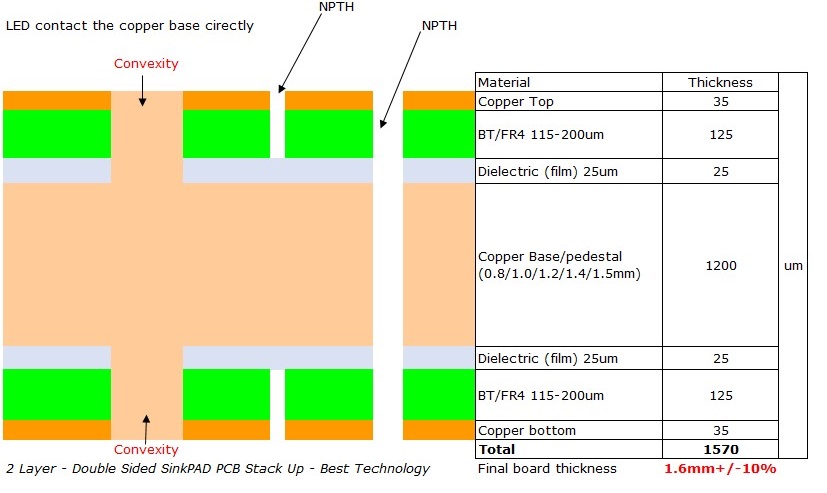
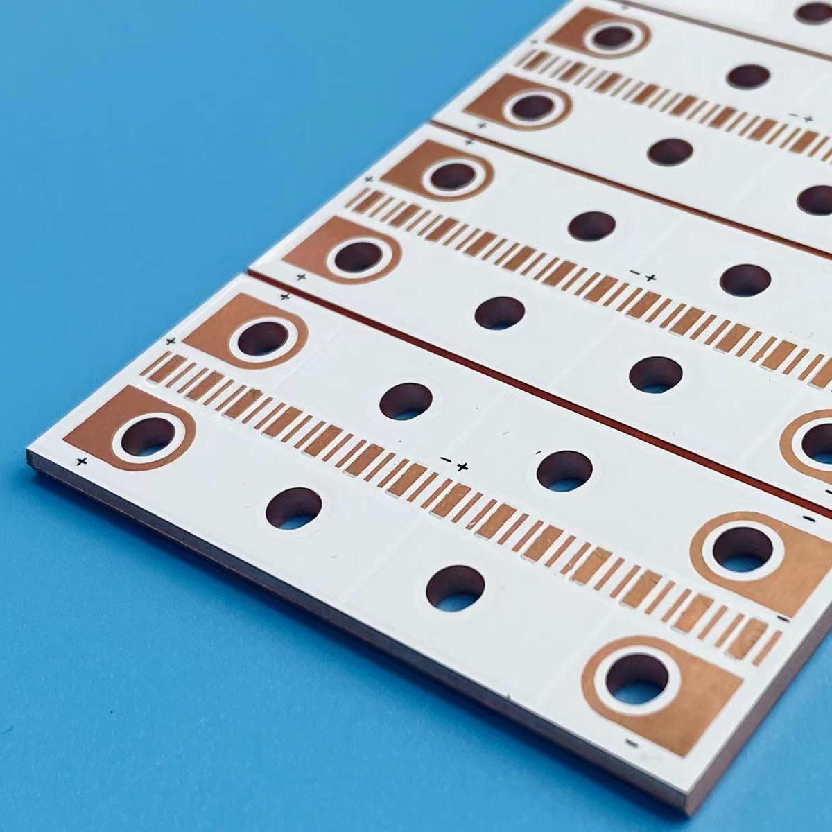
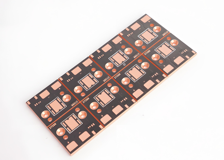
The Double sided SinkPAD board consists of at least two layers of trace circuit, and there’re at least one circuit layer on both top and bottom side of board, a dielectric (non-conducting) layer, a metal core/pedestal which normally is copper.
As there’re circuit layer on both sides, so engineer can put more (about 2 times, ideally) components on the same size circuit to realize more function, more complicated design, comparing to 1 Layer SinkPAD board or 2 layers SinkPAD board.
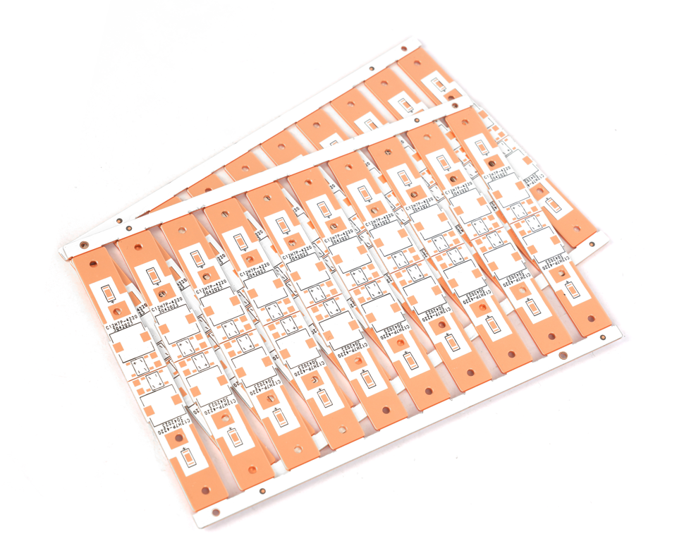
Double Sided SinkPAD Board
There’s no PTH (plated through hole) on double sided SinkPAD board, because the limitation of manufacturing process, which different from double sided Metal Core PCB which has a lot of PTH, and thermal PAD of LED will be put directly on copper core, also belonging to Direct Thermal Path (DTP) board too, but engineer needs to consider where the heat sink will be if he want more fast heat transferring, as there’re always components on both sides, and that make double sides SinkPAD board designing becoming more difficult & complex comparing to 1L SinkPAD board, or 2L SinkPAD board.
Stack up of Double Sided SinkPAD Board
Advantages of Utilizing Double Sided SinkPAD Board:
Put more components on the both top and bottom, design more complicated circuit board.
It adopts the thermoelectric separation structure, the Lumens depreciation of the LED is minimized, and the life of the lamp is prolonged.
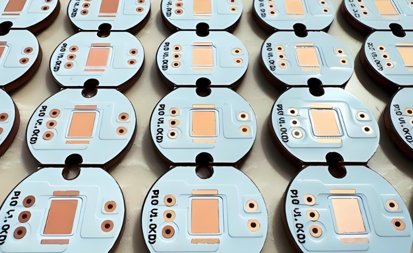
Suitable for matching single high-power lamp, such as Cree XPL, XML, XHP; Osram LED, etc., also COB package LED
High power semiconductors (transistors, thyristors, diodes) as well as resistors.
A variety of Surface Finishing are available according to different demands. (ENIG, OSP, Immersion Tin, ENEPIG, HAL) with excellent reliability of the surface treatment layer.
Application of Double Sided SinkPAD Board
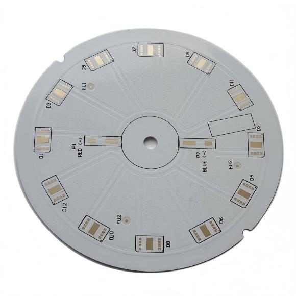
High Power LED (up to 200W).
High semiconductors (transistors, thyristors, diodes) as well as resistors.
2 Layer SinkaPAD Board Capability
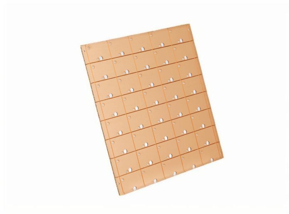
Base material: Copper: 0.8mm, 1.0mm, 1.2mm, 1.4mm, 1.5mm
If you want to customize double sided SinkPAD board, please contact EBest Circuit (Best Technology) today send your request for double sides SinkPAD PCB.
FAQs about Double-Sided SinkPAD Boards
1. What is a Double-Sided SinkPAD Board and how does it work?
A Double-Sided SinkPAD Board is a specialized Metal Core PCB (MCPCB) that provides a Direct Thermal Path (DTP) on both sides of the board. Unlike standard MCPCBs that use a dielectric layer to separate the circuit from the metal base, SinkPAD technology removes the dielectric under the component’s thermal pad. This allows the component (like a high-power LED) to sit directly on the copper or aluminum core, drastically reducing thermal resistance.
2. How does a Double-Sided SinkPAD differ from a standard Double-Sided MCPCB?
The primary difference is the thermal conductivity. In a standard double-sided MCPCB, heat must travel through a thermally conductive dielectric layer (typically 1–8 W/m·K) to reach the metal core. In a SinkPAD board, the dielectric is bypassed entirely for the thermal pad, allowing for conductivity ratings as high as 400 W/m·K (if using a copper core). Additionally, double-sided SinkPADs allow for higher component density by utilizing both the top and bottom layers for active circuitry.
3. Why would I choose a double-sided design over a single-layer SinkPAD?
Engineers choose double-sided SinkPADs when they need to maximize functional density in compact spaces. It allows for roughly twice the component population or more complex circuit routing compared to a 1-layer board. This is ideal for high-power applications where you need to mount LEDs or transistors on one side while placing control circuitry, connectors, or additional power components on the other.
4. Are there limitations to the Plated Through Holes (PTH) in double-sided SinkPADs?
Yes. Due to the unique manufacturing process where the metal core is “sunk” or embossed to meet the trace layer, standard Plated Through Holes (PTH) are often limited or more complex to implement than in traditional FR4 boards. Connections between sides are typically handled through specialized routing or assembly techniques, so it is crucial to consult with your manufacturer during the design phase to ensure the layout is compatible with the “thermoelectric separation” structure.
5. Which base material is better for SinkPAD boards: Aluminum or Copper?
Copper: Best for ultra-high-power applications. It offers superior thermal conductivity (approx. 400 W/m·K) and is the most common choice for SinkPAD convexity because it is easier to etch and process for this specific technology.
Aluminum: More cost-effective and lighter. While it has good thermal properties, the chemical process for creating the SinkPAD convexity is more complex, often making it more expensive or difficult to produce than copper-based SinkPADs.
6. Can SinkPAD technology be used for components other than LEDs?
Absolutely. While most commonly used for high-power LEDs (Cree, Osram, etc.) to prevent lumen depreciation, SinkPAD boards are excellent for any high-power semiconductor that features an electrically neutral thermal pad. This includes power transistors, thyristors, diodes, and high-wattage resistors used in automotive, aerospace, or industrial power monitoring.
Electronic devices continue to shrink while power density keeps rising. Excess heat can shorten component life, reduce performance, and cause signal instability. Because of this, designers often select metal core PCB material instead of conventional laminates when thermal control becomes critical.
A metal core circuit board integrates a thermally conductive metal base beneath the dielectric and copper circuitry. This structure creates a direct path for heat to travel away from components. Compared with standard FR-4 boards, metal core PCBs can dissipate heat more efficiently and maintain better thermal balance during operation.
These boards are widely used in high-power LED lighting, automotive electronics, power converters, industrial control systems, and communication equipment. As power levels increase and device footprints shrink, engineers increasingly rely on aluminium core PCB, copper core PCB, and IMS PCB (Insulated Metal Substrate) technologies to stabilize thermal performance.
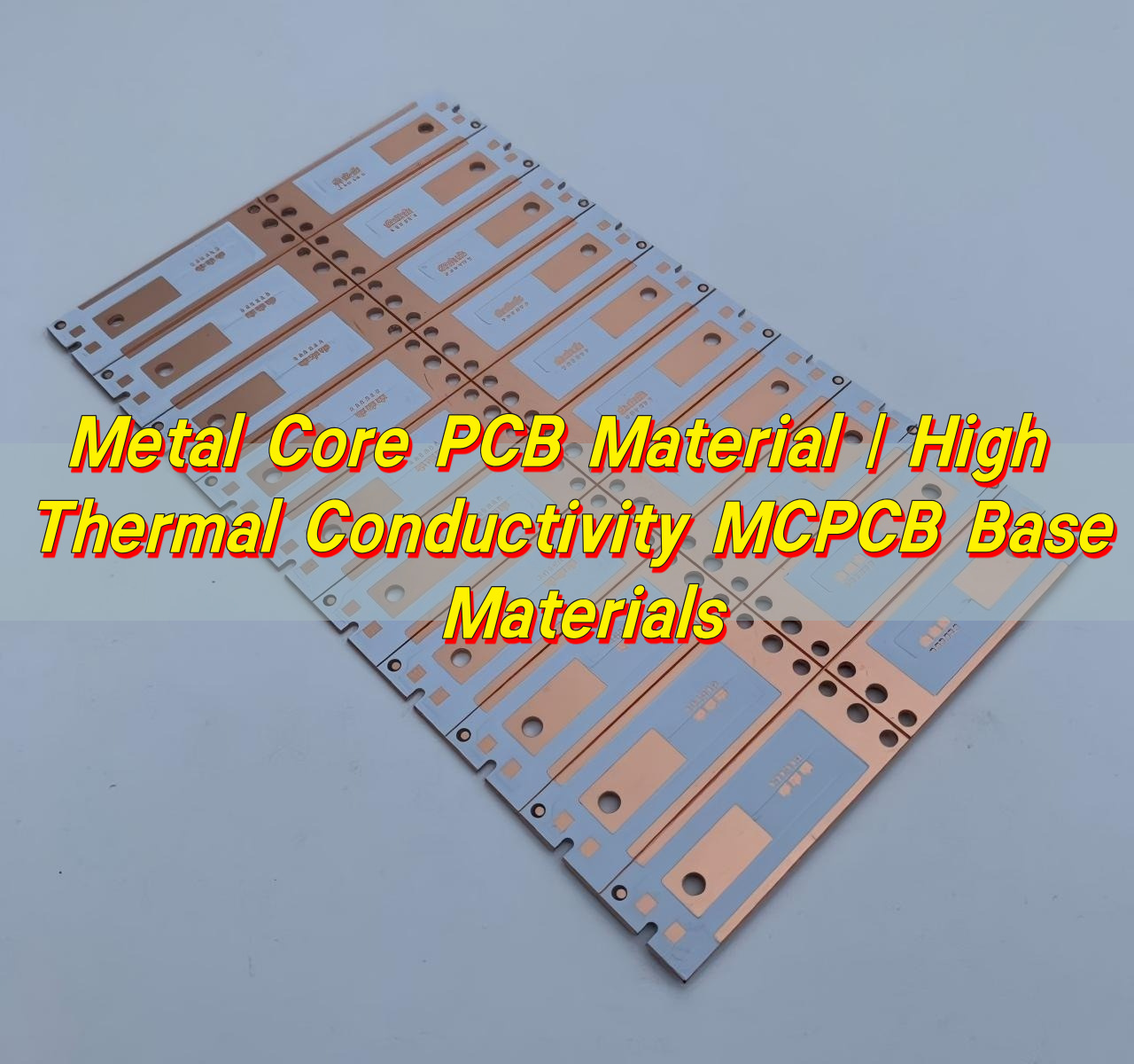
EBest Circuit (Best Technology)’s metal core PCB material provides excellent thermal conductivity, high stability and reliable performance for LED, power and high‑heat electronic applications.
What materials are used in metal core PCB?
A typical metal core PCB material structure consists of three primary layers. These layers work together to transfer heat efficiently from components to the metal substrate. Each layer performs a specific thermal and electrical function that ensures stable circuit performance.
The typical MCPCB stack structure includes:
Copper circuit layer
Thermal dielectric layer
Metal base layer
1. Copper Circuit Layer
The top layer contains copper traces that form the electrical circuit. This layer functions similarly to the copper layer in standard PCBs. Thicker copper improves current carrying capability and also spreads heat across the board surface. Copper thickness usually ranges from:
Copper Thickness
Typical Use
1 oz (35 μm)
Standard LED and low-power circuits
2 oz (70 μm)
Power LED modules
3 oz – 4 oz
High-current power electronics
2. Thermal Dielectric Layer
The dielectric layer is a critical part of metal core PCB material. It electrically isolates the circuit from the metal base while still allowing heat to pass through. High thermal conductivity dielectric materials allow heat to move quickly from components into the metal base. Typical dielectric properties include:
Property
Typical Range
Thermal conductivity
1 W/mK – 10 W/mK
Thickness
50 μm – 150 μm
Breakdown voltage
2 kV – 6 kV
Common dielectric fillers include:
Ceramic particles
Aluminum oxide
Silicon compounds
These fillers increase thermal conductivity while maintaining insulation strength.
3. Metal Base Layer
The bottom layer of a pcb metal core acts as the primary heat sink. It spreads heat over a large surface area and transfers it to the external environment. Aluminum is widely used because it provides strong thermal performance at a reasonable cost. Copper offers the highest thermal conductivity but is heavier and more expensive. The most common base materials are:
Metal Base Type
Thermal Conductivity
Aluminum
~200 W/mK
Copper
~385 W/mK
Steel
~50 W/mK
How to choose metal core PCB material?
Selecting the right metal core pcb material depends on several engineering factors. The design must balance thermal performance, mechanical strength, electrical insulation, and manufacturing cost.
1. Thermal conductivity requirement
Heat dissipation is the main reason for using IMS PCB technology. The thermal conductivity of the dielectric layer determines how quickly heat moves into the metal base. Higher conductivity improves cooling performance. Typical ranges include:
Thermal Conductivity
Application
1–2 W/mK
Standard LED lighting
3–5 W/mK
Automotive lighting
5–10 W/mK
High-power electronics
2. Electrical insulation performance
Although the metal base conducts heat well, it must remain electrically isolated from the circuit layer. Reliable insulation prevents short circuits and protects sensitive components. Designers must verify:
Dielectric breakdown voltage
Insulation resistance
Long-term reliability under temperature cycling
3. Mechanical stability
Mechanical strength is also important when selecting metal core PCB materials. Aluminum substrates provide good rigidity while keeping board weight low. Copper base boards offer superior strength but increase overall board mass.
4. Manufacturing compatibility
Manufacturers evaluate whether the material supports standard processes such as:
SMT assembly
reflow soldering
drilling and routing
surface finishing
A stable material simplifies production and improves yield.
What material is the MCPCB made of?
An MCPCB (Metal Core Printed Circuit Board) typically combines three major materials: copper circuitry, thermal dielectric, and a metal substrate. However, within this structure, several variants exist depending on the application.
Aluminum Core PCB
An aluminium core PCB is the most widely used type of MCPCB. Aluminum offers excellent thermal conductivity while remaining lightweight and cost-effective. Typical aluminum grades used include:
5052 aluminum
6061 aluminum
1060 aluminum
Advantages of aluminum core PCB include:
Lightweight structure
Good heat dissipation
Low material cost
Stable mechanical properties
Because of these benefits, aluminum core boards dominate LED lighting and power modules.
Copper Core PCB
A copper core PCB uses a solid copper substrate instead of aluminum. Copper has almost double the thermal conductivity of aluminum. This allows heat to move even faster away from components. However, copper boards are heavier and more expensive. Copper core PCBs are often used in:
high-power LEDs
RF power amplifiers
motor drivers
automotive electronics
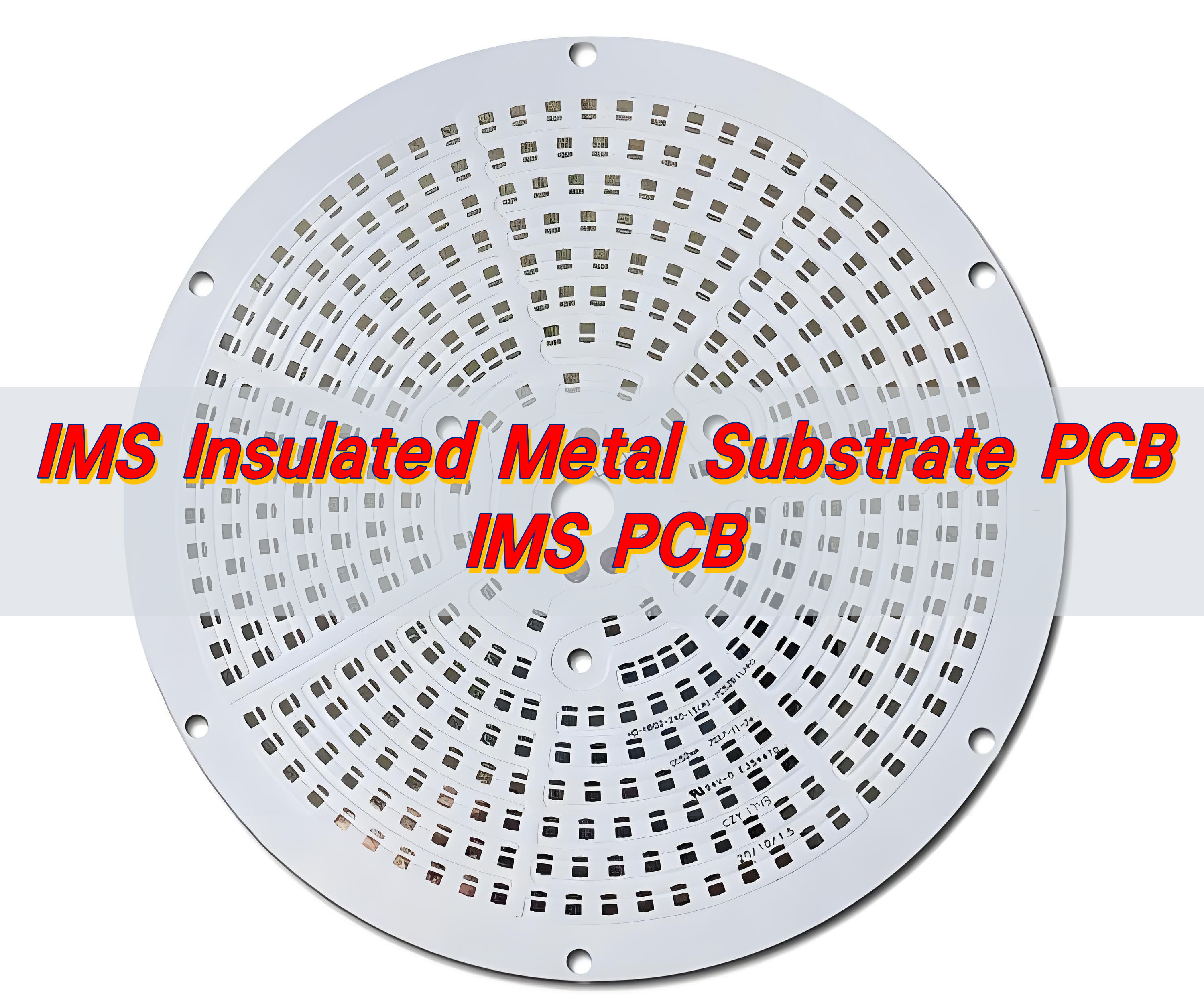
IMS PCB (Insulated Metal Substrate)
An IMS PCB refers to a board where a dielectric layer isolates the circuit from the metal base. Most metal core PCBs fall into this category. The IMS structure allows designers to combine electrical insulation with thermal efficiency.
The metal core pcb thickness varies depending on the design requirements. Engineers must consider both electrical performance and heat transfer efficiency. A typical MCPCB includes several thickness parameters.
Total board thickness. Thicker boards often improve mechanical strength. Common board thickness values include:
Board Thickness
Application
1.0 mm
Thin LED modules
1.6 mm
Standard MCPCB
2.0 mm
High-power lighting
3.2 mm
Power electronics
Metal core thickness. The metal base itself can vary significantly. A thicker metal base improves heat spreading capacity.
Metal Core Thickness
Typical Range
Aluminum base
0.8 mm – 3.0 mm
Copper base
1.0 mm – 4.0 mm
Dielectric thickness. The dielectric layer usually ranges between: 50 μm – 150 μm. A thinner dielectric improves thermal transfer but must still provide reliable electrical insulation.
Why is thermal conductivity important in metal core PCB material?
Thermal conductivity determines how quickly heat moves through a material. In electronic circuits, efficient heat removal protects components and stabilizes performance. High temperatures can reduce LED brightness, affect semiconductor switching speed, and shorten component lifespan.
A well-designed metal core PCB material structure solves this problem by creating a direct thermal path. Because the metal base spreads heat efficiently, the board avoids localized hot spots.
Heat flows through the following stages:
Component generates heat
Heat enters copper circuit layer
Heat moves through dielectric layer
Heat spreads across metal substrate
Heat dissipates into air or heat sink
Typical thermal conductivity comparison:
Material
Thermal Conductivity
FR-4
0.3 W/mK
Aluminum base
~200 W/mK
Copper base
~385 W/mK
What are benefits of metal core PCB material?
The advantages of metal core pcb materials extend beyond thermal performance. Engineers often select them because they improve reliability and design flexibility. Several benefits stand out. These advantages make pcb metal core technology suitable for high-power electronics.
1. Excellent heat dissipation
Metal substrates rapidly transfer heat away from components. This reduces thermal stress and improves long-term reliability.
2. Improved circuit stability
Stable temperatures keep semiconductor devices operating within their optimal range.
3. High mechanical strength
Metal substrates increase board rigidity and durability.
4. Compact product design
Efficient heat transfer allows designers to place components closer together.
5. Longer product lifespan
Lower operating temperature helps protect LEDs, ICs, and power components.
6. Reduced external cooling requirements
Many MCPCB designs operate without large heat sinks.
What is the difference between metal core PCB and FR4?
A metal core PCB vs FR4 comparison highlights the fundamental differences between the two technologies.
FR-4 is a fiberglass epoxy laminate commonly used in conventional PCBs. While it offers good electrical insulation, it has limited thermal conductivity. Metal core boards replace the fiberglass base with a thermally conductive metal substrate. In applications with high power density, metal core circuit boards offer clear advantages.
Below is a comparison of the two materials.
Feature
Metal Core PCB
FR-4 PCB
Base material
Aluminum or copper
Glass fiber epoxy
Thermal conductivity
High
Low
Heat dissipation
Excellent
Limited
Mechanical strength
Strong
Moderate
Weight
Heavier
Lightweight
Typical applications
LEDs, power electronics
Consumer electronics
Where is metal core PCB material used?
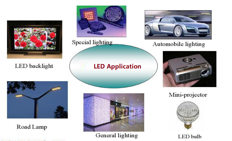
Because of its thermal advantages, metal core PCB material appears in many modern electronic systems. Industries rely on MCPCBs to manage heat in compact designs. Common applications include:
LED lighting, High-power LEDs generate substantial heat. MCPCBs help maintain consistent brightness and extend LED life.
Examples include:
street lighting
automotive headlights
industrial lighting
Automotive electronics, Vehicles require reliable thermal management for components such as:
engine control modules
power converters
lighting systems
Power electronics, Power supplies and converters generate high heat density. Metal core boards stabilize thermal performance in:
motor drives
DC-DC converters
industrial power modules
Communication systems, RF amplifiers and communication equipment often use copper core PCB structures to dissipate heat from power devices.
Consumer electronics, Compact devices such as projectors and audio equipment also benefit from MCPCB technology.
At EBest Circuit (Best Technology), we specialize in manufacturing high-quality metal core PCBs and thermal management circuit boards for demanding applications. Our engineering team supports customers from design review to production, ensuring each board meets strict performance standards.
Are you always curious these questions about insulated metal substrate PCB:
What is insulated metal substrate? Does it the same as metal core PCB (MCPCB)?
What are the key differences between insulated metal substrate and standard PCB?
Can I use insulated metal substrate in my project? What’s its performance?
As a experienced PCB manufacturer, we can confident to say the insulated metal substrate (IMS) PCB is the same as mcpcb, there is no differences between them. But it is big differ from standard PCB. Actually, IMS PCB offer numerous benefits in high power or heat sensitive projects. In this blog we will introduce what is it, its performance and the differeces with FR4 PCB.
What is an Insulated Metal Substrate (IMS)?
An insulated metal substrate (IMS) is a type of metal core PCB designed for heat-intensive applications. Unlike traditional FR4 boards, IMS uses a metal base layer—usually aluminum or copper—covered with a thin dielectric insulation and a copper circuit layer on top.
The purpose of this design is simple: dissipate heat quickly while keeping the circuit stable. Aluminum IMS boards are most common, offering a balance of cost, strength, and thermal conductivity. Copper IMS is used where performance is critical, especially in high-current applications.
Key characteristics of IMS PCBs include:
High thermal conductivity to transfer heat away from components.
Strong mechanical stability compared to FR4.
Reliable performance in harsh environments.
For industries like LED lighting, automotive electronics, and power supplies, IMS PCBs have become a preferred choice.
What is IMS material for PCB?
The performance and cost of an insulated metal substrate PCB depend heavily on the choice of the base material. Different metals give different levels of thermal conductivity, mechanical strength, and pricing.
1. Copper IMS PCB
Copper has the best thermal conductivity among IMS options. It spreads heat rapidly and is highly stable under load. However, copper is expensive, so it is often reserved for high-power applications such as industrial converters or advanced automotive modules.
2. Aluminum IMS PCB
Aluminum is the most common choice for IMS PCBs. It strikes a balance between cost, weight, and thermal performance. With good heat dissipation and lower price than copper, it has become the preferred material in LED lighting and consumer automotive systems.
3. Iron IMS PCB
Iron-based substrates are rarely used. While they are strong, their lower thermal performance and processing challenges make them less attractive. In most cases, aluminum and copper dominate the IMS market.
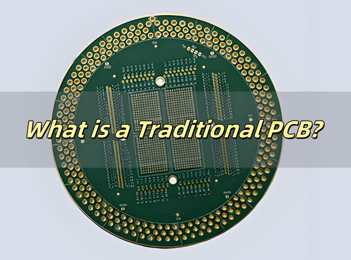
What is a Traditional PCB?
A traditional PCB typically refers to a board made with FR4 substrate. FR-4 is a code for a fire-resistant material grade. It represents a material specification where the resin material must be able to extinguish itself when exposed to a burning condition. It is not a material name but a material grade. Most consumer electronics use FR4 PCBs because they are affordable and easy to manufacture.
The construction includes:
Fiberglass base (FR4) for insulation and strength.
Copper foil laminated on one or both sides.
Solder mask and silkscreen for protection and labeling.
FR4 PCBs work well in devices that do not generate extreme heat. They are versatile and suitable for phones, laptops, IoT devices, wearables, and household appliances.
What is the Difference Between Insulated Metal Substrate and PCB?
The key differences between ims pcb and traditional PCB is the base material, IMS pcb uses metal core as the base substrate while traditional PCB uses fiberglass epoxy. Due to the differences base materials used, their performance, price and applications are different accordingly. Here we listing a detailed table for your reference:
Feature
Traditional PCB (FR4)
Insulated Metal Substrate (IMS)
Base Material
Fiberglass epoxy (FR4)
Metal base (aluminum or copper)
Thermal Conductivity
Low (~0.3 W/mK)
High (2–10 W/mK dielectric + metal base can reach up to 400 W/mk)
Heat Management
Needs extra cooling (heat sinks, fans)
Built-in heat spreading through metal layer
Mechanical Strength
Rigid but less durable under vibration
Strong, resists shock and vibration
Flexibility
Can be rigid, flex, or rigid-flex
Mostly rigid only
Applications
Consumer electronics, IoT, computers
LED lighting, automotive, power modules
Cost
Low, highly economical for mass production
Higher, due to materials and processing
Why is IMS Better for Heat Dissipation Compared to PCB?
As we all know, heat is the biggest enemy of electronic components. If heat builds up, components degrade, solder joints crack, and lifespan shortens. Standard FR4 struggles to move heat away, leading to performance issues in high-power systems.
An IMS PCB solves this by using a metal base that acts like a built-in heat sink. The dielectric layer transfers heat from components directly to the metal, which spreads it out quickly. This keeps the board and devices cooler and improves the overall reliability.
This is why IMS PCBs are widely used in LED lighting, where heat directly impacts brightness and lifespan. Similarly, automotive systems like motor controllers and power converters use IMS to handle constant high currents.
Which Applications Do We Use IMS vs Standard PCB?
Each type of board has its own application areas.
IMS PCB applications
LED lighting systems
Automotive electronics (engine control units, sensors, chargers)
Power modules and converters
Industrial motor drives
Telecom base stations
FR4 PCB applications
Consumer electronics (phones, tablets, laptops)
IoT devices and smart wearables
Household appliances
Audio and multimedia systems
Office electronics
The decision depends on the heat level, power density, and cost balance.
Cost Differences Between IMS and PCB
IMS PCBs are more expensive than standard FR-4 boards due to their raw materials and processing steps. Aluminum-based IMS typically costs $0.12–$0.25 per cm², while FR-4 falls around $0.05–$0.10 per cm². Extra copper thickness, dielectric layers, and specialized drilling add further expense.
Yet, the higher upfront cost can translate into system savings. In LED lighting, automotive, and power modules, IMS often reduces the need for heat sinks or cooling parts. Studies show a 15–20% drop in overall system cost when FR-4 is replaced with IMS, thanks to better thermal control and longer product life.
Design Consideration of Insulated Metal Substrate PCB
Designing an Insulated Metal Substrate (IMS) PCB is more than just replacing FR4 with a metal base. The entire design strategy changes because thermal performance becomes the top priority. Several aspects need careful thought:
1. Dielectric Layer Thickness and Thermal Conductivity
The dielectric is the heart of an IMS PCB. Its job is to provide electrical insulation while transferring heat from the copper layer to the metal base.
Typical FR4 dielectric has thermal conductivity of 0.3–0.5 W/mK.
IMS dielectrics range from 2 to 10 W/mK, depending on material choice.
Thickness is usually 50–150 μm. Thinner layers transfer heat better but risk breakdown if not well controlled.
For normal LED boards, a 75 μm dielectric with 1-2 W/mK conductivity is often a balance between cost and reliability.
2. Copper Thickness and Trace Design
Current capacity is vital. Wider traces reduce resistance and heat buildup.
Standard FR4 PCBs often use 1 oz (35 μm) copper.
IMS boards commonly use 2–3 oz (70–105 μm) copper to carry higher currents.
IPC-2221 guidelines suggest that a 2 oz copper trace at 10 mm width can handle around 20–25 A continuously, which fits the demands of power devices.
3. Component Placement and Thermal Management
Hot components, such as MOSFETs, LEDs, or regulators, should be placed directly over areas where heat can spread into the metal base efficiently. Grouping high-power parts together without proper spacing often leads to localized hot spots.
Simulation tools (like ANSYS or thermal CAD software) are often used to map temperature rise. Data shows that placing components 5 mm apart can reduce local heat rise by 8–12°C compared to tightly packed layouts.
4. Board Thickness and Mechanical Strength
IMS boards are stiffer than FR4 due to the metal layer.
Common thickness: 0.8–3.2 mm.
For automotive PCBs exposed to vibration, a 1.6 mm aluminum base is typical for balancing rigidity and weight.
Designers should consider mounting holes and mechanical supports early to avoid stress cracking during assembly.
5. Surface Finishes and Soldering
Surface finishes like ENIG, ENEPIG, OSP or HASL are commonly applied. However, IMS boards undergo more thermal cycling during soldering, so ENIG is often preferred for reliability.
Factors Affect the Failure of Insulated Metal Substrate PCB
Even with proper design, IMS PCBs can fail if certain risks are not controlled. Failures usually stem from thermal, mechanical, or environmental stresses. Let’s examine the main causes, with supporting data:
1. Thermal Stress and Cycling
IMS PCBs are exposed to wide temperature swings, especially in LED lighting (-40°C to +120°C) or automotive control units (-55°C to +150°C). In additional, a thinner dielectric layer (<75 μm) is more likely to fail under repeated expansion and contraction. So, using high Tg dielectrics (Tg ≥ 170°C) and flexible solder materials reduces the chance of cracks.
2. Dielectric Breakdown
The dielectric layer separates copper circuitry from the conductive metal base. If the insulation fails, short circuits occur.
Standard IMS dielectric breakdown voltage: 2–6 kV/mm.
If the dielectric is too thin or contaminated during manufacturing, breakdown may occur earlier, especially in high-voltage power supplies.
3. Corrosion and Moisture Ingress
If the protective coating or solder mask is not properly applied, moisture, chemicals, or salts can corrode the copper traces or the aluminum base. There is no doubt that unprotected copper can corrode in under 72 hours in a salt spray environment (5% NaCl). Therefore, applying ENIG or OSP surface finishes greatly reduces corrosion risk.
4. Mechanical Stress and Vibration
IMS boards are less flexible than FR4, which means they can crack under excessive bending or vibration.
In automotive vibration testing (10–2,000 Hz sweep, 20 g), poor mounting caused delamination in 5–10% of samples after 50 hours.
Poor drilling, lamination errors, or uneven dielectric spreading can lead to early failures. For example:
Misaligned lamination can create voids, which increase heat resistance and raise local temperatures by 10–15°C.
Improper drilling of vias in IMS can leave burrs or microcracks, leading to premature electrical failure.
EBest Circuit (Best Technology) has more than 19 years in IMS PCB manufacturing. It cannot be denied that we had ever faced such problems and solved them finally, then we have much experiences to solve them and mature skills to avoid such defectives.
Insulated Metal Substrates Market
The insulated metal substrates market has grown rapidly with the demand for efficient heat management in electronics. Several sectors drive this expansion:
LED Lighting: As LEDs move into general lighting, street lamps, and automotive headlights, IMS boards remain essential for heat control.
Electric Vehicles (EVs): Motor controllers, inverters, and battery systems require durable IMS boards to handle high currents.
Industrial Power Systems: Power converters, motor drives, and renewable energy inverters are major adopters.
Telecom: Base stations and 5G equipment rely on IMS to stabilize performance under heavy workloads.
Market reports suggest steady growth in IMS adoption worldwide, especially in Asia-Pacific regions like China and South Korea, where LED and EV industries are booming. Aluminum IMS PCBs dominate due to cost efficiency, but copper IMS is growing in high-performance niches.
How to Choose Between IMS PCB and FR4 PCB?
The choice between IMS PCB and FR-4 PCB depends on performance demands, cost expectations, and application environment. If your design handles high power density or generates significant heat—such as in LED lighting, power converters, or automotive control units—IMS PCB is usually the better option. Its aluminum or copper base provides strong thermal conductivity, keeping component temperatures 20–30% lower than FR-4 under the same load.
FR-4 PCB, on the other hand, is more suitable for general-purpose electronics where heat generation is moderate. Devices like consumer gadgets, IoT sensors, and low-power communication modules often prioritize affordability and flexibility in design over extreme thermal performance. FR-4 also supports higher multilayer counts more easily than IMS, which is beneficial for complex circuits with dense routing.
So, in a word:
Choose FR4 PCB if your device is low-power, cost-sensitive, and not heat-intensive.
Choose IMS PCB if your design generates high heat, requires high reliability, or operates in harsh environments.
In practice, many manufacturers use both types in their product lines. Consumer electronics stay with FR4, while lighting and automotive turn to IMS.
FAQs
1. What materials are used in insulated metal substrates?
IMS PCBs usually use aluminum or copper as the base, with a dielectric insulation layer and copper foil.
2. Is IMS PCB more reliable than FR4 PCB?
Yes, especially in high-power or high-heat applications, IMS offers better thermal management and durability.
3. Can IMS replace all standard PCBs?
No, IMS is designed for specific heat-demanding uses. FR4 remains more cost-effective for everyday electronics.
4. Why are IMS PCBs used in LED lighting?
They transfer heat away quickly, improving brightness, efficiency, and lifespan of LEDs.
5. How expensive are IMS PCBs compared to normal PCBs?
IMS PCBs cost more due to metal materials and manufacturing, but they often save costs by reducing cooling needs.
About EBest Circuit (Best Technology) – Your Trust Insulated Metal Substrate PCB Supplier
EBest Circuit (Best Technology) is a turnkey PCB & PCBA manufacturer in China, we specialize in the design and manufacturing of high-quality PCBs, and we are confident that we can provide a tailored solution for your project. With our expertise and a broad range of materials, including SY, Rogers, Isola, KB, ceramic, metal core pcb, flex circuit and busbar copper pcb, etc, we offer flexibility and reliability for all your PCB designs.
We’ve made many PCBs for our customers, whether you need high-speed, high-frequency, or multi-layer PCBs, our experienced engineering team ensures reliable, cost-effective designs with excellent manufacturability. We’ve worked in this industry over 19 years, so we deeply know what our customers want, and make them into reality.
Our services include:
Customized PCB design based on your schematic and specifications
Free Design for manufacturability (DFM) to reduce production issues
Optimization for signal integrity, thermal management, and reliability
PCB layout and PCB design full turnkey service
Industry certifications we have:
ISO9001 (quality management system)
IATF16949 (for automotive device)
ISO13485 (for medical instrument)
AS9100D (aerospace applications)
In addition to our advanced PCB manufacturing capabilities, we also have a fully equipped SMT factory both in China & Vietnam. This facility is dedicated to providing our customers with professional PCB assembly services, including SMD soldering, component placement, and testing. This allows us to offer a complete solution, from PCB fabrication to final assembly, all under one roof. If you have PCB or IMS PCB manufacturing demands, welcome to contact us at sales@bestpcbs.com
Unlike traditional PCBs that rely on FR4 or other resin-based materials, IMS PCBs use a metal base—typically aluminum or copper. This base is paired with a dielectric layer and a copper circuit layer on top.
It’s not just a circuit board. It’s a thermal solution that keeps devices cool and running longer.
IMS PCB full form and meaning?
The full form of IMS PCB is Insulated Metal Substrate Printed Circuit Board. It’s a PCB built to move heat away from components. That means better reliability, higher efficiency, and longer lifespan for your electronic products.
In this type of PCB, the metal substrate acts as a heat spreader. The insulation layer isolates the copper circuit from the metal base, while still allowing heat to pass through. It’s a smart design that balances performance with thermal control.
What is IMS material?
The core of every IMS PCB lies in its materials. These layers provide the best thermal and electrical performance. Here’s what you’ll find in a standard IMS stack:
Metal Base Layer: Usually aluminum for cost-efficiency and light weight. Copper is also used when more heat dissipation is required.
Dielectric Layer: A thermally conductive but electrically insulating material. It transfers heat from the circuit layer to the metal base.
Copper Circuit Layer: This is where the actual electrical routing happens. It’s similar to traditional PCB copper layers but optimized for thermal contact.
These three layers form the structure of IMS. The combination is compact, efficient, and powerful—especially in LED lighting, automotive electronics, and power converters.
The insulation layer, in particular, must handle high thermal loads while resisting electrical breakdown. Advanced IMS designs often use proprietary dielectric materials to increase thermal conductivity and reduce overall thickness.
How thick is a IMS PCB?
The thickness of an IMS PCB depends on the application. But typically, here’s what you can expect:
Metal base layer: 0.5mm to 3.2mm
Dielectric layer: 0.03mm to 0.2mm
Copper layer: 0.035mm to 0.2mm
The total thickness usually ranges from 0.8mm to 3.5mm. For LED lighting and compact modules, thinner IMS boards (like 1mm) are common. But in power-heavy designs, thicker boards provide the support and thermal capacity needed.
Some custom builds even exceed 3.5mm if the heat demands are extreme. A thicker aluminum layer enhances mechanical strength and heat dissipation, but it also increases weight and cost. So choosing the right thickness is a balance of thermal needs and design efficiency.
What is the difference between FR4 and IMS PCB?
FR4 PCBs use glass-reinforced epoxy as their core. They are great for general electronics. But FR4 struggles with thermal stress. When high-power components run hot, FR4 doesn’t cool them fast enough. That leads to overheating and failure.
IMS PCBs, on the other hand, are built for thermal performance. The metal base acts like a built-in heat sink. It draws heat away from critical components and spreads it out. That protects the electronics and improves reliability.
Feature
FR4 PCB
IMS PCB
Core Material
Epoxy-based fiberglass
Metal (usually aluminum)
Thermal Conductivity
~0.25 W/mK
1.0–9.0 W/mK or more
Heat Dissipation
Limited
Excellent
Cost
Lower
Slightly higher, but worth it
Mechanical Strength
Moderate
Stronger due to metal core
For everyday consumer electronics, FR4 is fine. But for power-hungry devices, IMS PCBs offer unmatched reliability.
2 layer IMS PCB vs Multilayer IMS PCB
While single-layer IMS boards are most common, especially in LED lighting, 2-layer and multilayer IMS PCBs are gaining ground in complex applications.
2-layer IMS PCB means there are copper circuits on both sides of the dielectric layer, with one metal core layer. These offer more routing options while still allowing good heat dissipation.
Multilayer IMS PCBs, on the other hand, can include several copper layers, separated by insulation, and only one side is connected to the metal base for heat transfer. This allows for complex routing and high component density while keeping thermal control.
Benefits of 2-layer IMS PCB:
Better circuit flexibility
Moderate thermal management
More design freedom
Benefits of Multilayer IMS PCB:
High circuit complexity
Suitable for dense power modules
Thermal performance still superior to FR4
If you’re building a simple LED module, a single or 2-layer IMS may be enough. But if you’re designing a power controller, communication device, or automotive ECU, multilayer IMS is often necessary.
IMS PCB stackup: What to know?
Stackup design is more than just layers, it defines how your board handles heat, power, and performance. A typical IMS PCB stackup looks like this:
Copper circuit layer
Dielectric insulation layer
Metal substrate (usually aluminum)
But there’s room for customization. Here’s what matters:
Copper thickness: Choose 1oz, 2oz, or more depending on current flow.
Dielectric performance: The higher the thermal conductivity (measured in W/mK), the better the heat transfer.
Metal base: Aluminum is the go-to for most. But copper or stainless steel can be used for extreme performance or rigidity.
Surface finish: Choose between HASL, ENIG, OSP, or others based on your assembly process.
Stackup choices directly affect reliability. A poor choice here means components will overheat, solder joints will crack, or performance will drop.
What are the applications of IMS PCB?
IMS PCB is widely used in high power industry.
LED lighting: Keeps high-brightness LEDs cool, extending their life.
Automotive electronics: Used in headlights, sensors, battery modules.
Power converters: Manages heat in inverters and converters.
Industrial control systems: Ensures smooth performance under high power loads.
Communication base stations: Maintains signal integrity and prevents thermal breakdown.
Why choose the right IMS PCB Manufacturer?
At EBest Circuit (Best Technology), we understand the critical role IMS PCBs play. We’ve spent years perfecting the production process, materials, and stackup customization. Every board we deliver is tested for:
Thermal conductivity
Mechanical strength
Electrical reliability
Whether you need standard single-layer boards or complex multilayer IMS PCBs, we can build it to your exact needs.
Conclusion:
IMS PCB is very important in high power electronics. From simple LED lights to advanced power modules, IMS boards keep your devices cool, stable, and efficient.
Looking for an IMS PCB manufacturer you can rely on? Contact us today at sales@bestpcbs.com
Why choose copper IMS PCB? This guide covers copper IMS PCB from design to manufacturing, highlighting superior heat dissipation, design guidelines for high-power applications, and EBest Circuit (Best Technology)’s precision production capabilities.
Are you bothered by these problems?
How to break through the heat dissipation bottleneck?
How to balance cost and performance?
How to ensure signal integrity?
EBest Circuit (Best Technology) can provide:
Three-dimensional heat dissipation architecture: Exclusive copper-based composite design, thermal resistance reduced by 40%, achieving a 25°C reduction in temperature rise at the same power consumption.
Optimized material cost performance: Patented copper-aluminum hybrid process, reducing material costs by 18% while maintaining thermal conductivity.
Electromagnetic compatibility integration: Built-in gradient impedance design, 5G band signal attenuation is controlled within 0.3dB.
Welcome to contact us if you have any inquiry for metal core PCB: sales@bestpcbs.com.
What Is Copper IMS PCB?
Copper IMS PCB (Insulated Metal Substrate Printed Circuit Board) is a high-performance circuit substrate constructed on a metal base (typically copper or aluminum) coated with a thermally conductive dielectric layer. It combines a copper circuit layer, a ceramic/polymer-based insulating layer, and a metal core to achieve exceptional thermal management (1-12 W/m/K conductivity), electrical insulation, and mechanical stability. Primarily used in high-power applications like LED lighting, automotive power modules, and aerospace systems, it offers 100x lower thermal resistance than FR4 while enabling efficient heat dissipation through its metal core structure.
What Is Stackup of Copper IMS PCB?
Copper IMS PCB Stackup Structure
Copper Base Plate
Material: High-purity electrolytic or rolled annealed copper (1–5 oz thickness) for superior thermal conductivity (398 W/m·K).
Function: Primary heat dissipation layer, often embedded with thermal vias to enhance heat transfer to external heat sinks.
Dielectric Insulation Layer
Material: Ceramic-filled epoxy or high-thermal-conductivity prepreg (e.g., 0.15 mm thickness with thermal resistance <0.7°C/W).
Function: Provides electrical isolation between the copper circuit and base plate while minimizing thermal resistance.
Copper Circuit Layer
Material: Thin copper foil (0.5–2 oz) for signal/power routing, processed via etching to form circuits.
Function: Conductive pathways for components, with optimized thickness balancing current capacity and signal integrity.
Solder Mask & Surface Finish (Optional)
Solder Mask: Protects copper traces and prevents solder bridging.
Surface Finish: ENIG (Electroless Nickel Immersion Gold) or HASL (Hot Air Solder Leveling) for solderability and oxidation resistance.
Design Considerations
Symmetry: Mirror-stacked layers (e.g., L1/L4, L2/L3) to prevent warping.
Thermal Vias: Embedded or plated-through vias to connect heat-generating components to the copper base.
Material Selection: High-Tg (>170°C) prepreg for stability under thermal cycling.
Exceptional Current Carrying Capacity (15A/mm²) – Supports 3x higher current density than standard FR4, reducing PCB size by 35% for equivalent power.
Thermal Expansion Matching (CTE=17ppm/℃) – Eliminates solder joint failures in thermal cycling (-40°C to 150°C), critical for automotive/industrial apps.
Built-in EMI Shielding – Reduces RF noise by 40dB without additional shielding layers, ideal for 5G/RF circuits.
High-Frequency Performance – Superior signal integrity for GHz-range applications with minimal signal loss.
Miniaturization Potential – Supports 0.1mm dielectric layers and microvias for chip-scale packaging in medical/portable devices.
Long-Term Reliability – Zero oxidation risk and 100% recyclability reduce lifetime costs by 18% vs. aluminum.
What Are Applications of Copper IMS PCB?
Automotive: Reduces overheating in LEDs/batteries – longer lifespan, lower maintenance.
Renewable Energy: Cuts heat loss in solar/wind systems – boosts efficiency, lowers costs.
Use thick copper foil (2oz/3oz or higher) to handle high current densities.
Prioritize low-thermal-resistance dielectric layers (e.g., ceramic-filled polymers) to maximize heat transfer to the copper base.
2. Thermal Management
Place heat-generating components (e.g., MOSFETs, LEDs) directly over the copper base for direct heat dissipation.
Add thermal vias under hot components to channel heat vertically to the copper layer.
Avoid thermal isolation; ensure continuous copper paths for heat flow.
3. Current Path Optimization
Design wide, short traces for high-current paths to minimize resistance and I²R losses.
Use parallel traces or polygon pours to distribute current evenly.
Avoid sharp bends (≥90°) in high-current traces to reduce inductance and hotspots.
4. Layer Stackup
Prioritize a 2-layer stack: copper base (bottom), dielectric layer, and copper top layer.
For complex designs, add internal copper layers with prepreg insulation, ensuring thermal vias connect all layers.
5. Mechanical Stability
Maintain symmetry in layer stackup to reduce warping during reflow.
Use heavy copper (≥3oz) for rigid base support; avoid over-etching thin features.
6. Component Placement
Isolate high-power components from sensitive analog/digital sections to prevent thermal interference.
Leave spacing around heat sinks or mounting holes for airflow or mechanical fixation.
7. Testing & Validation
Perform thermal simulation (e.g., ANSYS Icepak) to verify heat dissipation under max load.
Test under worst-case power conditions to ensure junction temps stay below component limits.
Notes: Balance thermal performance, electrical efficiency, and mechanical reliability. Prioritize direct heat paths, robust current handling, and material durability for high-power resilience.
Copper IMS PCB Manufacturing Processes
1. Material Preparation: Start with a copper base plate, a thermally conductive dielectric layer (e.g., ceramic-filled polymer), and top-layer copper foil. Materials are selected for thermal performance and durability.
2. Lamination: Bond the layers under controlled heat and pressure. The copper base, dielectric, and top foil are fused to create a rigid, thermally efficient structure.
3. Drilling: Precision-drill vias and through-holes. Clean debris thoroughly to ensure clean plating surfaces.
4. Plating: Apply electroless or electrolytic copper plating to coat hole walls, enabling vertical electrical connections between layers.
5. Etching: Use photoresist and chemical etching to remove excess copper from the top layer, leaving defined circuit traces.
6. Surface Finish: Apply finishes like ENIG, OSP, or immersion silver to protect exposed copper and enhance solderability during assembly.
7. Cutting & Profiling: Cut the panel into individual PCBs. Machine edges (e.g., V-score, routing) to meet required dimensions and shapes.
8. Quality Testing: Perform electrical tests (continuity, isolation), thermal stress tests (e.g., reflow cycles), and visual inspections to ensure reliability and performance.
Are you worried about how to chooseIMS PCB materialfor your project? Let’s explore its definition, properties, datasheet, types, IMS PCB material selection and design guidelines through this blog.
Wrong choice of substrate material leads to too high thermal resistance?
Is the dielectric layer easy to delaminate during multi-layer IMS design?
Is the dielectric loss too large under high-frequency application?
EBest Circuit (Best Technology) Can Provide:
Provide 5 standardized thermal conductivity levels (1.5~8W/mK); Free sample matching tool, generate selection report in 30 minutes.
Patented resin system, peel strength>1.8N/mm; Support 3-layer lamination process, provide design specification manual.
Df value as low as 0.002 (@10GHz); Equipped with HFSS simulation model library, plug-and-play.
IMS material, known asinsulated metal substrate, consists of a metal core, typically aluminum or copper, coated with a dielectric insulation layer and a conductive copper layer for circuit traces. This structure delivers outstanding thermal management, with aluminum-based versions achieving thermal conductivity of 1-3 W/(m·K), while copper-based variants exceed 400 W/(m·K) for accelerated heat dissipation.
It serves effectively in high-power applications like LED lighting systems and automotive electronics, where efficient cooling maintains device stability and extends operational lifespan under thermal stress.
IMS PCB Material Properties
Thermal Conductivity – Metal base (aluminum/copper) transfers heat 5-10x faster than FR4, keeping components cooler.
Electrical Insulation– Dielectric layer provides high voltage isolation (1-10kV) while allowing heat flow.
Mechanical Strength – Metal core resists bending/warping, ideal for heavy components or high-vibration environments.
Clarify power density (W/cm²), operating environment (temperature/humidity), space limits, and budget. Example: Automotive ECU board needing 50A current handling in 100°C engine bay.
Design Rules: Minimum trace width/spacing ≥0.2mm for aluminum IMS; ≥0.15mm for copper IMS.
Solder Mask: Remove mask in thermal zones to maximize metal exposure.
Panelization: Add 2mm border around boards for handling during assembly.
7. Validation & Testing
Thermal Imaging: Test under max load to identify hotspots. Junction temp should stay ≤85°C.
Electrical Testing: Verify current capacity and signal integrity (e.g., <5% voltage drop).
Reliability Testing: Conduct thermal cycling (-40°C to +125°C, 100 cycles) and vibration tests (2G RMS).
IMS PCB Board Design Considerations
Thermal Management
Base Material Selection: Aluminum (1-3 W/mK) suits cost-sensitive, moderate-heat applications like LED lighting. Copper (>400 W/mK) is ideal for high-power modules requiring rapid heat dissipation.
Dielectric Thickness: Thinner layers (50-100μm) improve heat transfer but reduce voltage isolation. Match thickness to operational voltage (e.g., 100μm for <1kV).
Component Placement: Position high-heat components (e.g., power ICs, LEDs) directly over the metal core to maximize thermal path efficiency.
Electrical Performance
Trace Width/Spacing: Wider traces reduce resistance for high-current paths. Maintain ≥0.3mm spacing for 1kV isolation in standard designs.
Via Usage: Avoid thermal vias in the dielectric layer, they disrupt heat flow. Route signals through peripheral non-metal zones.
High-Frequency Limits: IMS materials exhibit higher dielectric loss than FR-4. Limit use in RF circuits (>500MHz).
Mechanical Design
Board Thickness: Standard metal cores (1.0-3.0mm) prevent flexing but increase weight. For lightweight needs, consider 1.0mm aluminum.
Mounting Hardware: Use insulated standoffs to prevent short circuits with the metal base. Account for CTE mismatch, aluminum expands 23ppm/°C versus 17ppm/°C for copper.
Confirm Thermal Management Expertise: Verify experience with aluminum/copper cores and UL-certified dielectric materials for effective heat dissipation in high-power applications.
Demand Precision Manufacturing Capabilities: Ensure ≤50μm laser drilling accuracy for microvias and tight tolerances (±25μm) critical for thermal performance.
Require Relevant Quality Certifications: Prioritize IATF 16949 (automotive) or ISO 13485 (medical) certified suppliers with documented thermal cycling tests (-40°C to +150°C).
Evaluate True Production Speed: Compare realistic lead times. Proven manufacturers deliver prototypes in 7 days, 30% faster than industry norms without compromising quality.
Insist on Transparent Costing: Avoid hidden fees. Competitive suppliers offer fixed pricing with 5-15% savings through efficient material utilization.
Check Scalability from Prototype to Volume: Choose partners handling orders from 5 panels to mass production seamlessly within their facilities.
Prioritize Technical Partnership: Select manufacturers providing free 24-hour DFM feedback and thermal simulation support to optimize your design.
Experience the EBest Circuit (Best Technology) Advantage: Get a rapid quote for your IMS PCB project today. We combine certified quality, 7-day prototype turnaround, and cost-competitive pricing—ensuring your thermal management solution excels. Request your quote now.
Ready to start your project? Contact EBest Circuit (Best Technology) today for competitive pricing, guaranteed fast delivery, and certified quality. Let’s optimize your thermal management solution together: sales@bestpcbs.com.
IMS PCB full form is Insulated Metal Substrate PCB—a type of printed circuit board built to manage high heat and maintain strong mechanical support. It’s a popular choice for LED lighting, power supplies, and automotive electronics, where heat control is critical.
At EBest Circuit (Best Technology), we’re a trusted IMS PCB manufacturer in China, providing custom thermal management solutions with high precision, reliable materials, and a full range of engineering support. But let’s dig deeper into what makes insulated metal substrate PCBs unique—and why they’re so important in modern electronics.
What Is IMS Insulated Metal Substrate PCB?
An IMS (Insulated Metal Substrate) PCB is a type of circuit board that uses a thermally conductive dielectric layer bonded between a metal base (often aluminum or copper) and a copper circuit layer. The metal base helps dissipate heat more efficiently, especially compared to traditional FR4 boards.
When it comes to IMS PCB thermal conductivity, this is the most valuable feature. The dielectric layer in IMS boards typically offers a thermal conductivity range from 1.0 W/mK to over 8.0 W/mK, depending on the application. The metal base, like aluminum or copper, works as a built-in heat sink—pulling heat away from active components like LEDs, power transistors, or ICs. That’s why IMS PCBs are commonly used in LED modules, power converters, automotive lighting, and solar inverters—where both heat and performance need to be tightly controlled.
IMS PCB Material
Choosing the right material for an IMS board is essential. Three layers make up a standard IMS PCB: the metal base, the dielectric layer, and the copper foil. And for the metal base, there are two options: copper base and aluminum base.
Copper IMS PCB
Copper IMS PCBs offer superior heat transfer capabilities. Copper has a thermal conductivity of nearly 400 W/mK, much higher than aluminum. This means copper is ideal for applications with extreme power densities or where space is limited but heat is a concern.
However, copper is also more expensive and heavier than aluminum, so it’s generally reserved for high-performance needs like laser modules, RF circuits, or military-grade devices.
IMS Aluminum PCB
The IMS aluminum PCB is the most common choice. Aluminum provides good thermal conductivity (typically around 200 W/mK), excellent mechanical strength, and lower cost compared to copper.
Aluminum IMS PCBs are often used in LED lighting systems, electric vehicle chargers, power control modules, and industrial automation systems. They provide a balanced solution between cost and thermal management, which is why they’re the industry standard. Some common aluminum grades used include:
5052 aluminum: Strong, corrosion-resistant, and suitable for structural use.
6061 aluminum: Versatile, high-strength alloy.
1060 aluminum: Excellent thermal conductivity, ideal for cost-sensitive applications.
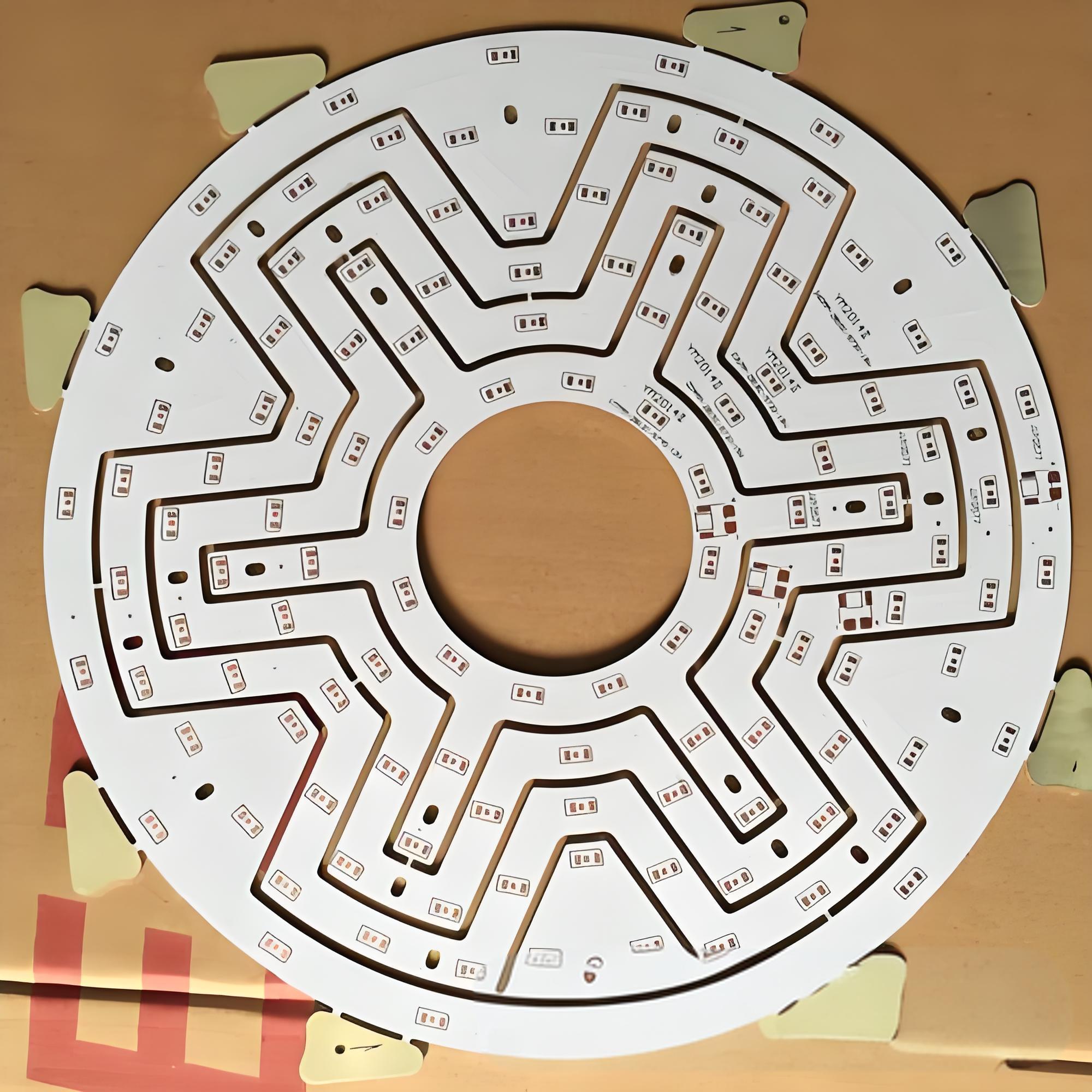
IMS PCB Stackup
The stack-up of an IMS PCB refers to how the layers are arranged. A typical IMS PCB stackup includes:
Top copper trace layer – for routing signals and power.
Thermal dielectric layer – usually made of epoxy resin filled with ceramic for heat transfer.
Metal base – usually aluminum or copper.
For more advanced applications, 2 layer IMS PCBs are often used. In a 2 layer IMS PCB, an additional copper circuit layer is placed above the dielectric, and interconnections are formed using plated through-holes. These are useful when you need more complex routing or higher power density.
Multilayer IMS stackups are possible but require special lamination techniques. These are often customized depending on the mechanical, electrical, and thermal needs of the application.
IMS PCB Applications
Thanks to their excellent thermal performance and mechanical strength, IMS PCBs are widely used in demanding environments. Here are some key application areas:
LED lighting: Street lights, high-bay lights, grow lights, automotive headlights.
Power electronics: DC-DC converters, voltage regulators, motor drivers.
Automotive systems: Electric vehicle controllers, battery management units.
Telecommunication: 5G base stations, power amplifiers.
Renewable energy: Solar panel inverters, wind turbine converters.
IMS PCB HS Codes
For companies that export or import IMS PCBs, understanding HS codes (Harmonized System codes) is essential for customs clearance and compliance.
The general HS Code for IMS PCB falls under:
8534.00 – Printed Circuits
Subcategories can vary depending on whether the board is populated (assembled) or bare.
To be more precise:
a. Bare IMS PCBs (unassembled):
HS Code 8534.00.90 (for 1-4 layer ims pcb)
HS Code 8534.00.10 (4 or above layer ims pcb)
b. Assembled IMS PCBs:
HS Code 8537.10 or others depending on final product classification and applications.
Always check with your local customs authority or logistics provider for the exact code applicable to your product type and destination country.
IMS PCB Assembly
IMS PCB assembly involves more care than standard FR4 boards due to thermal management and mechanical rigidity. Special attention must be given to soldering profiles and thermal expansion to prevent cracking or delamination.
Key points during assembly:
Use low-stress soldering methods (e.g., vapor phase or controlled reflow).
Ensure proper thermal profile during reflow to avoid damage to the metal base or insulation.
Choose high-Tg solder masks and components to handle high power density applications.
For high-volume needs, automated SMT lines should be optimized for heat dissipation and tight placement tolerances.
DFM (design for manufacturability) & DFA (design for assembly) checks
SMT and through-hole soldering
AOI, X-ray inspection
Functional testing
Box building assembly
Final inspection
Our strict quality control ensures your boards are built to meet thermal and mechanical demands.
Best IMS PCB Manufacturer – EBest Circuit (Best Technology)
When choosing an IMS PCB manufacturer, experience, quality, and customization capabilities matter most. That’s where EBest Circuit (Best Technology) stands out.
We specialize in insulated metal substrate PCBs with over a decade of industry focus. Our strength lies in advanced thermal management PCBs, from aluminum IMS boards to copper-core multilayer solutions.
Why Choose EBest Circuit (Best Technology) for IMS PCBs?
✅ Technical Support Before & After Sales
✅ 99% Customer Satisfaction ISO9001, ISO13485, IATF16949, UL
✅ Material options: Wide range of metal bases (Al, Cu, Stainless Steel), dielectric materials with 1–8 W/mK.
✅ Full-stack service: From DFM support to final assembly and testing.
✅ MES traceability: Real-time tracking and control throughout production.
Whether you need a 2 layer IMS PCB for automotive lighting or a high-power copper IMS board for industrial drives, we can tailor the solution to fit your needs. With our strong supply chain and experienced team, we help customers worldwide bring their designs to life.
EBest Circuit (Best Technology) is your go-to partner for custom IMS PCB fabrication and assembly. We combine deep technical knowledge, certified quality, and flexible manufacturing to deliver solutions that work—every time.
Ready to upgrade your thermal management? Contact EBest Circuit (Best Technology) today for a quick quote or technical consultation.
FAQs
1. What is the difference between IMS PCB and FR4 PCB?
IMS PCBs use a metal base for better heat dissipation, while FR4 boards use fiberglass, which has low thermal conductivity.
2. Can IMS PCBs be multilayered?
Yes, multilayer IMS PCBs are possible but require special lamination techniques and are more complex to manufacture.
3. What are typical thermal conductivity values for IMS PCBs?
The dielectric layer in IMS boards usually ranges from 1 to 8 W/mK. Copper and aluminum also contribute to heat dissipation.
4. What is the HS code for an assembled IMS PCB?
Typically, 8537.10, but check with local customs authorities as codes can vary by region.
5. How can I request a custom IMS PCB quote from EBest Circuit (Best Technology)?
Simply email us your Gerber files, BOM, and design requirements, or use our online quote form. Our engineers will get back to you quickly.