

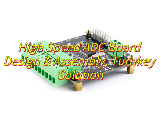
What is high speed ADC board? Let’s discover its components, types, benefits, application, design and assembly processes and recommended assembly service supplier.
Are you troubled with these problems?
- Signal integrity issues? High-frequency interference messing up ADC sampling, raising test costs?
- Prototyping delays? Spotting design flaws late, holding up projects?
- Welding yield low? Tiny parts having defects, slowing production?
EBest Circuit (Best Technology) can provide you service and solution:
- Full SI simulation: See signal loss clearly from design to product.
- 72-hour fast prototyping: With DFM review and backup plans.
- Micro-spacing welding: Custom solutions, guaranteeing 85%+ first-article yield.
Welcome to contact us if you have any request for high speed ADC board assembly: sales@bestpcbs.com.
What Is High Speed ADC Board?
A High Speed ADC Board is an electronic hardware device designed to convert high-frequency analog signals (such as radio waves, laser pulses, or rapidly changing sensor outputs) into digital data within extremely short timeframes.
Its core function is to capture instantaneous signal details through ultra-fast sampling (billions of samples per second) and integrate signal conditioning circuits with high-speed data interfaces to ensure rapid, accurate data transmission to processors or storage systems.
What Are Components of High Speed ADC Board?
- ADC Chip: Core component converting analog to digital signals, supporting high sampling rates (GS/s) and resolution (12-16 bits).
- Analog Front-End Circuitry: Preprocesses signals with amplifiers, filters, and buffers to reduce noise and match ADC range.
- Clock Management System: Provides low-jitter, synchronized clocks via precision sources and distribution networks.
- Power Supply Subsystem: Supplies clean, stable voltage using regulators and filters to minimize noise impact.
- Digital Interface Module: High-speed interfaces (e.g., LVDS, JESD204B/C) connect ADC to processors for data transmission.
- Control Logic Unit: Uses microcontroller/FPGA for ADC configuration, data management, and real-time control.
- PCB: Multi-layer design with high-speed routing, impedance matching (50Ω), and grounding to reduce interference.
- Thermal Management: Includes heat sinks or fans to dissipate heat for stable operation.
- Connectors: External ports (e.g., SMA, BNC) for signal access and system integration.
- Memory Module (Optional): FIFO buffer RAM for temporary data storage to prevent overflow.
What Are Types of High Speed ADC Boards?
General-Purpose High-Speed Data Acquisition Boards:
- Features: Versatile, with GS/s sampling and 12 – 14-bit resolution.
- Applications: Lab tests, industrial data collection, and research like signal and sensor analysis.
ADC Boards for Communication Systems:
- Features: Optimized for 5G/LTE, with high-speed serial interfaces (JESD204B/C) for low-latency data transfer. High dynamic range and anti-interference.
- Application: Base stations and RF front-end modules.
ADC Boards for Radar & Imaging:
- Features: Used in radar, medical imaging (MRI/ultrasound), and military. High-frequency processing (>10 GS/s) and low noise. Built-in FPGAs for real-time processing, support pulse compression and image reconstruction.
- Applications: Radar signal and medical imaging processing.
FPGA-Integrated ADC Boards:
- Features: Combine high-speed ADCs with FPGAs (Xilinx/Intel). Flexible interfaces (FMC/HSMC) for custom logic.
- Application: AI acceleration and embedded system development.
PCIe High-Speed ADC Cards:
- Features: Connect via PCIe for >10 Gbps data transfer.
- Application: PC-based data collection like audio/video testing and production line monitoring.
Networked Remote ADC Modules:
- Features: Support Ethernet/Wi-Fi for distributed data and IoT. Low power and remote control.
- Application: Wireless signal monitoring and remote experiments.
Customized ADC Boards:
- Features: Designed for special needs like aerospace. Optimized for size, power, or temperature. Radiation-resistant for extreme conditions.
- Application: Data collection in harsh environments.
What Are Advantages of High Speed ADC Board?
- Low Power Consumption Design: Employs open-loop amplification or monotonic capacitor switching techniques, reducing power consumption by 60% – 81%.
- High Dynamic Performance: Supports a high signal-to-noise and distortion ratio (SNDR ≥ 57 dB) and has low total harmonic distortion (THD ≤ -76 dB), meeting the requirements of precision measurement applications.
- Simplified System Integration: Integrates a digital output buffer (supporting a 0.5V low-voltage interface) and on-chip decoupling capacitors, minimizing the number of required external components.
- Strong Scalability: Provides standardized interfaces (such as FMC connectors), facilitating easy integration with FPGA platforms.
What Are Applications of High Speed ADC Board?
Communication
- 5G base stations handle high-speed and high-frequency analog signal transmission.
- Satellite communication ground stations receive and demodulate weak satellite signals.
- Optical fiber communication equipment converts analog electrical signals after optical reception.
Radar
- Military air defense radars identify air target information.
- Weather monitoring radars grasp precipitation and storm changes.
- Automotive anti-collision radars judge the danger of obstacles ahead.
Medical
- CT scanners generate images of internal human body structures.
- Ultrasound diagnostic instruments display dynamic images of human organs.
- MRI equipment constructs high-resolution images of human tissues.
Aerospace
- Aircraft navigation systems calculate flight attitude, position, and speed.
- Spacecraft telemetry systems monitor operational status parameters.
Scientific Research
- Particle accelerator experiments record particle collision information.
- High-energy physics experiments obtain precise data of weak signals.
How to Design High Speed ADC Evaluation Board?
1. Power Design Considerations
Isolation & Decoupling:
- Use separate power domains (AVDD, DVDD, CLKVDD) to prevent digital noise coupling.
- Place multi-stage decoupling capacitors (0.1μF + 10μF + 100μF) near each power pin.
Power Sequencing:
- Follow the ADC’s specified power-up order (e.g., PVDD before DVDD) to avoid latch-up.
Noise Suppression:
- Add ferrite beads (e.g., BLM18PG) or inductors on LDO outputs for high-frequency isolation.
2. Clock Design Considerations
- Low-Jitter Source: Use a dedicated low-jitter clock (e.g., SiT9102) with jitter <10% of ADC aperture jitter.
- Distribution & Matching: Control differential clock impedance (100Ω ±10%) and match trace lengths (±50mil).
- Isolation: Keep clock traces away from digital signals and add AC coupling caps (0.1μF) at inputs.
3. Analog Signal Chain Considerations
- Impedance Matching: Design matching networks (T/π filters or transformers) for ADC input impedance (e.g., 50Ω).
- Anti-Aliasing Filter (AAF): Set cutoff at 0.4× sampling rate (80% Nyquist) and avoid high-order filters (>4 stages).
- Protection: Add clamping diodes (e.g., BAT54S) and keep analog traces short (<500mil) to minimize parasitics.
4. Digital Interface Considerations
- JESD204C/LVDS Optimization: Match differential pairs (100Ω) and add 100Ω termination resistors at receivers.
- Level Compatibility: Use level shifters (e.g., SN74AVC4T245) if ADC output (LVDS/CMOS) mismatches FPGA.
- Sync & Reset: Include SYNC~ signals for JESD204C synchronization and debounce reset circuits.
5. PCB Layout & Manufacturing
- Stackup & Partitioning: Use a 6-layer stackup (Sig-GND-Power-Power-GND-Sig) with analog/digital ground isolation.
- Critical Routing: Prefer blind/buried vias for high-speed signals and add stitching vias for impedance continuity.
- Thermal & Reliability: Add via arrays under ADC for heat dissipation and fill via-in-pads with conductive epoxy.
6. EMC & Testing
- EMC Protection: Use TVS diodes (e.g., SMAJ5.0A) for ESD and ferrite beads for power noise isolation.
- Test Points: Reserve test pads for power, clock, and analog inputs without probing high-speed lines directly.
- Temperature Compensation: Select low-drift references (e.g., ADR4525, ±5ppm/°C) and validate performance at extremes.
7. BOM & Supply Chain
- Component Selection: Prioritize automotive/industrial-grade parts (-40°C to +125°C) and validate alternatives via simulation.
- Lifecycle Management: Avoid obsolete parts (check Digi-Key) and use common packages (e.g., 0402) for cost efficiency.
- DFM: Add teardrops to pads and avoid 0201 packages for easier assembly.
How To Assemble High Speed ADC Development Board?
1. Prepare Tools and Workbench
- Clean the workbench: Clear the work area of clutter to create a clean and organized environment for assembly.
- Wear an antistatic wrist strap: Prevent damage to delicate electronic components from static electricity generated by the human body.
- Gather tools: Prepare precision screwdrivers, tweezers, a soldering iron (or hot air gun), flux, a desoldering pump, and a multimeter.
- Check components: Cross-reference the Bill of Materials (BOM) to ensure all required parts for assembly are present and that the tools are suitable for fine electronic work.
2. Verify Components and Circuit Board
- Component verification: Check each component’s model, specifications, and quantity against the BOM, including the ADC chip, power module, capacitors, resistors, and connectors.
- Board inspection: Examine the circuit board surface for scratches, shorts, or open circuits.
- Position alignment: Confirm that each component matches the corresponding pads on the board for accurate installation.
3. Solder Surface-Mount Components
Wear an antistatic wrist strap and solder components from smallest to largest:
- Solder small 0402/0603 resistors and capacitors using drag or spot soldering, avoiding bridges.
- For BGA-packaged ADC chips, apply flux to pads and heat using a hot air gun or reflow oven following the temperature profile to prevent localized overheating.
- When soldering QFN/LGA components, align pins carefully and use tweezers for support during soldering.
4. Install Through-Hole Components
For components like power connectors, headers, and switches, manual soldering is sufficient:
- Insert component leads into corresponding holes, heat pads from the back of the board, and remove the soldering iron promptly once the solder melts to keep leads upright.
- Trim excess leads to less than 1.5mm to prevent short circuits.
5. Connect External Modules and Interfaces
Install sub-boards or expansion modules (e.g., clock modules, signal conditioning circuits) as per design requirements:
- Secure modules with headers or connectors to ensure good contact.
- Control solder volume when soldering RF coaxial interfaces or high-speed differential lines to avoid signal distortion.
6. Preliminary Inspection and Cleaning
- Use a multimeter to test power lines, ground lines, and key signal lines for continuity, shorts, or opens.
- Clean flux residue and solder splatter from the board using alcohol and an antistatic brush to prevent long-term corrosion and poor contact.
7. Functional Testing and Debugging
- Connect power and an oscilloscope, power up gradually, and monitor voltage stability.
- Input test signals (e.g., sine waves, square waves) and use a logic analyzer or PC software to verify ADC sampling accuracy, signal-to-noise ratio (SNR), and other parameters against specifications.
- Adjust component parameters (e.g., matching resistors, decoupling capacitors) or optimize layout based on test results until performance meets requirements.
Why Choose EBest Circuit (Best Technology) as ADC Board Assembly Supplier?
Reasons why choose us as ADC board assembly supplier:
- Trusted Industry Leader: 19 years of experience and 500+ clients served, including medical, 5G, and precision instrumentation projects.
- Turnkey Solution: From design and component sourcing to PCB fabrication, SMT/DIP assembly, and testing, we streamline every step—cutting costs and speeding up delivery.
- Free DFM: Provide free DFM for optimizing high-speed layouts, power integrity, and signal conditioning for top-tier sampling accuracy and SNR performance.
- Precision SMT Production: Automated lines handle 0201/0402 components and complex packages (BGA/QFN) with 99.8%+ yield rates and AOI and X- Ray quality checks.
- Strict Quality Control: ISO 9001-certified, with 100% inspection of critical processes to ensure reliable boards.
- Flexible & Fast Manufacturing: Support small prototypes (50+ units) to large-scale runs (100K+/month), with 72-hour rapid prototyping for urgent needs.
- Custom Design Solutions: Tailored PCB stacking, EMC/EMI fixes, and thermal management for industrial, medical, and telecom applications.
- Cost-Effective & Stable Supply Chain: Long-term partnered with top suppliers to reduce BOM costs by 10–30% while securing stable component availability.
Welcome to contact us if you have any request for ADC board assembly service: sales@bestpcbs.com.