

How to design hermetic ceramic package? Let’s discover types, benefits, applications, design spec and guide, production process for hermetic ceramic package.
Are you worried about these problems?
- Does your chip’s lifespan and reliability suffer from moisture intrusion and corrosion in harsh environments?
- Is high-power chip performance constrained by heat buildup, limiting its full potential?
- Are miniaturization and high-frequency requirements restricted by packaging size and signal integrity limitations?
As a hermetic ceramic package manufacturer, EBest Circuit (Best Technology) can provide you service and solutions:
- Customized Solutions: Full-process collaborative development from material formulation to structural design, tailored to chip characteristics for stable operation across -55°C to 200°C temperature ranges.
- Thermal Management Optimization: High-thermal-conductivity ceramics (Al₂O₃/AlN) combined with thermal via arrays and metal heat sinks, reducing thermal resistance by 30% for 10W-class chips.
- High-Density Integration Support: HTCC/LTCC fine-pitch technology (0.5mm lead spacing, 50μm line/space) enabling compact packaging with maintained high-frequency performance and signal integrity.
Welcome to contact us if you have any inquiry for hermetic ceramic package: sales@bestpcbs.com.
What Is Hermetic Ceramic Package?
A hermetic ceramic package is a special ceramic housing used to encapsulate high-reliability electronic components such as chips, sensors, and MEMS. Its core lies in the tight bonding between the ceramic substrate and a metallized sealing structure (such as a cover plate or pins), forming a completely sealed cavity that blocks the penetration of external gases and moisture. This hermeticity ensures that the internal sensitive components are protected from contamination and degradation under harsh environments (high temperature, humidity, corrosion), thereby achieving long-term stable operation of the electronic device.
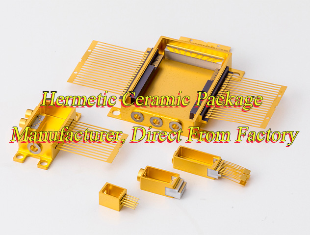
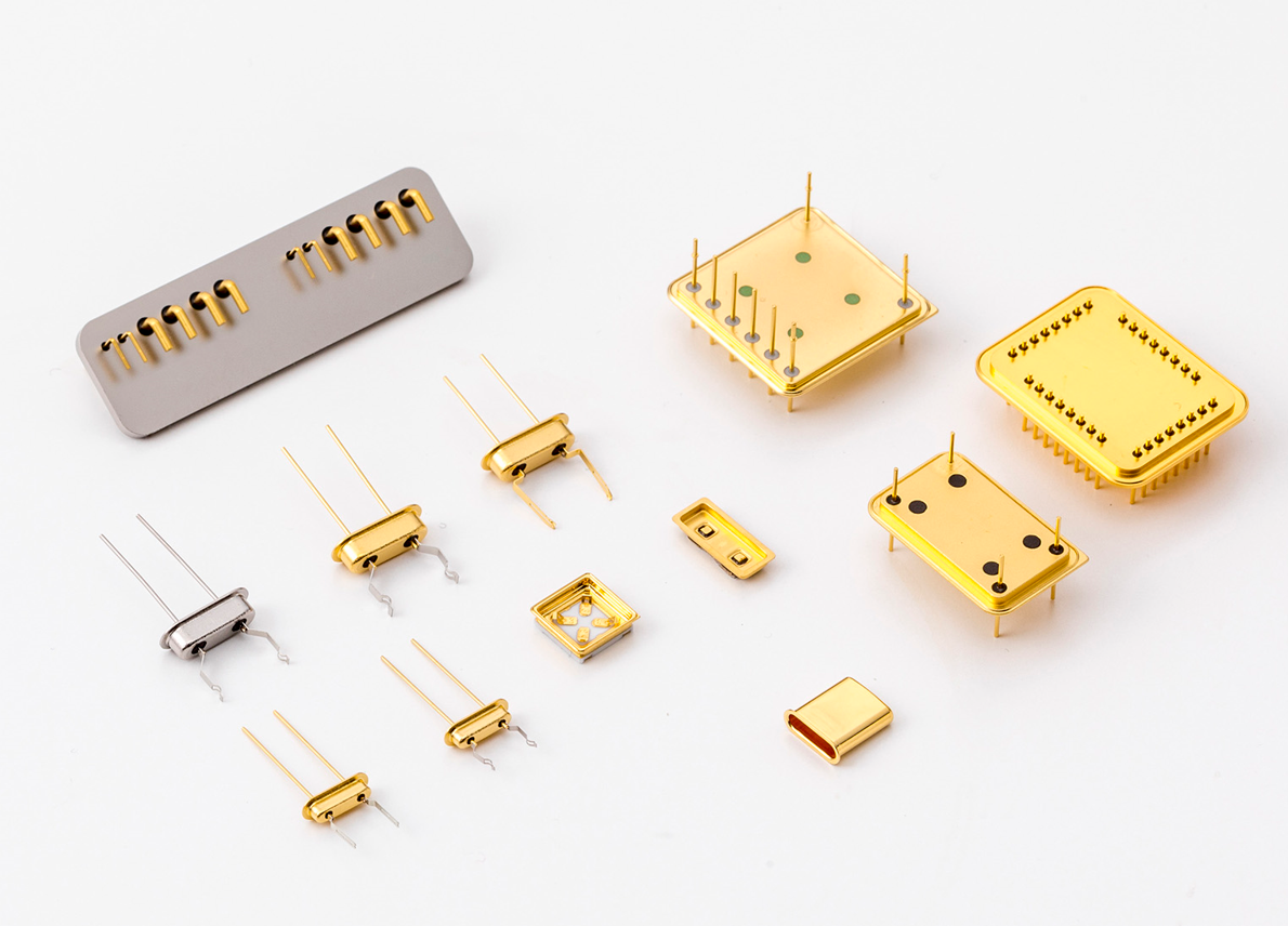
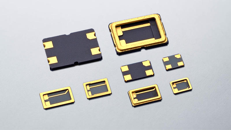
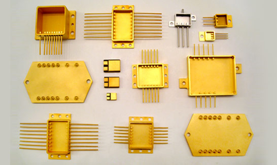
What Are Types of Hermetic Ceramic Packages?
Ceramic Dual In-line Package (CDIP)
- Structure: Two rows of parallel leads extend from both sides of the ceramic housing, with a typical lead pitch of 2.54 mm (0.1 inch).
- Features: Classic package form, easy to solder through-hole (THT), high mechanical strength.
- Applications: Early CPUs, memory, military standard devices, high-reliability analog circuits.
Ceramic Quad Flat Package (CQFP)
- Structure: Four outward-extending “gull-wing” leads on all four sides, with a typically small lead pitch (e.g., 0.5 mm, 0.65 mm, 0.8 mm).
- Features: High lead density, suitable for surface mount technology (SMT), good heat dissipation and electrical performance.
- Applications: High-frequency/RF devices, high-end processors, aerospace electronics.
Ceramic Leadless Chip Carrier (CLCC/LCCC)
- Structure: Metallized pads on all four sides (no external leads), directly connected to the PCB via solder. Mostly square in shape.
- Features: Small size, no lead stress issues, good vibration resistance, excellent high-frequency characteristics.
- Applications: Spacecraft, satellite payloads, high-reliability communication modules, MEMS sensor packaging.
Ceramic Pin Grid Array (CPGA)
- Structure: An array of vertically arranged pins (pin-shaped) on the bottom, soldered via sockets or through-holes.
- Features: High pin density, excellent electrical performance and heat dissipation (especially when paired with a metal cap or heatsink).
- Applications: High-performance CPUs, FPGAs, ASICs, and other devices requiring a large number of I/O pins and heat dissipation.
Ceramic Ball Grid Array (CBGA)
- Structure: An array of solder balls (replacing leads) is located at the bottom, allowing direct reflow soldering onto the PCB.
- Features: Extremely high I/O density, excellent electrothermal performance (low inductance, good heat dissipation path), but difficult to rework.
- Applications: VLSI, high-end graphics processors, network processors.
Ceramic Small Outline Package (CSOP)
- Structure: Similar to CQFP, but narrower and longer, with gull-wing leads on two or four sides (usually fewer pins than CQFP).
- Features: More space-saving than CDIP, suitable for surface mounting.
- Applications: Memory, medium-density logic devices.
What Are Advantages of Hermetic Ceramic Packages?
- Superior Hermeticity: Achieves absolute sealing via metal brazing or glass sealing processes, blocking moisture, dust, salt mist, chemical contaminants, and harmful gases. Internal environment controlled with dry inert gas (e.g., nitrogen) or vacuum for long-term stability.
- Extreme Environment Reliability: Operates across -55°C to +200°C+ temperature range (varies by ceramic type). Withstands high-pressure/vacuum environments in deep sea, aviation, and aerospace. Radiation-resistant for space applications. Resists mechanical shock and vibration via high-strength ceramic housing.
- Outstanding Material Properties: High insulation resistance (>10¹² Ω) prevents signal crosstalk and ensures safety for high-frequency/high-voltage devices. Thermal management via high-thermal-conductivity ceramics (e.g., AlN, 170-230 W/mK) efficiently dissipates chip heat. Low coefficient of thermal expansion (CTE) matches silicon chips to minimize thermal stress cracking. Chemically stable, corrosion-resistant, and oxidation-resistant.
- Superior Electrical Performance: Low dielectric constant and loss reduce signal delay, enhancing performance for high-frequency/radio-frequency devices (e.g., 5G, radar). Stable parasitic parameters prevent environmental drift of capacitance/inductance. Metal lids provide electromagnetic interference (EMI) shielding.
- Longevity and Durability: Decades-long lifespan in aerospace, medical implants, and other high-reliability fields. Ceramic materials avoid plasticizer evaporation, maintaining performance over time (superior to plastic packaging).
- Multi-Functional Integration Adaptability: Supports high-density interconnection via HTCC/LTCC processes, integrating passive components (resistors/capacitors). Compatible with optical windows (e.g., laser packaging) and RF feedthrough structures. Adaptable to various high-reliability package formats (DIP, QFP, BGA, LCC).
What Are Applications of Hermetic Ceramic Package?
- Satellites and Space Probes: Spacecraft control systems, onboard computers (radiation resistant, withstands drastic temperature changes in vacuum). High-precision sensors (e.g., gyroscopes, temperature sensors).
- Missiles and Radar Systems: Missile guidance chips (resistant to supersonic flight vibrations and high temperatures). Phased array radar T/R modules (high-frequency signal stability requirements).
- Avionics: Engine control units (ECUs), black box data recorders (shock resistant, fireproof).
- Life Support Implantable Devices: Pacemakers, nerve stimulators (absolutely sealed to prevent bodily fluid corrosion, lifespan > 10 years).
- Extracorporeal High-End Medical Devices: High-voltage sensors for MRI scanners, surgical robot control modules (electromagnetic interference resistant).
- Deep-Sea Drilling and Oil & Gas Extraction: Downhole sensors (resistant to 200°C high temperature, 170MPa high pressure, and hydrogen sulfide corrosion).
- Nuclear Power Plants and High-Radiation Environments: Reactor monitoring sensors (resistant to neutron/gamma-ray radiation).
- New Energy Power Systems: High-voltage IGBT modules (aluminum nitride substrate for heat dissipation, moisture-proof).
- Safety Core Systems: Airbag controller and brake control unit (withstanding temperature cycling from -40°C to 150°C).
- Electric vehicle power module: Silicon carbide (SiC) inverter package (high thermal conductivity AlN ceramic heat dissipation).
- 5G/6G RF front-end: Millimeter-wave power amplifier (low-loss ceramic substrate ensures high-frequency signal integrity).
- Optical communication module: Laser diode (LD) and photodetector (PD) package (dustproof and oxidation-proof optical path protection).
- Quantum computing device: Superconducting quantum bit chip package (maintained in ultra-vacuum/ultra-low temperature environments).
- High-precision sensor: MEMS inertial navigation unit (protected against moisture-induced drift errors).
Hermetic Ceramic Package Design Specification
| Technical Parameter | Specification |
| Hermeticity Standard | ≤1×10⁻⁸ atm·cc/s He |
| Internal Moisture Content | ≤100 ppm |
| Substrate Ceramic Type | Al₂O₃ / AlN / LTCC / HTCC |
| Thermal Conductivity | Al₂O₃: 20-30 W/mK ; AlN: 170-230 W/mK |
| Coefficient of Thermal Expansion (CTE) | Al₂O₃: 6-7 ppm/K ; AlN: 4-5 ppm/K |
| Dielectric Constant | Al₂O₃: 9-10 @1MHz ; LTCC: 5-8 @1GHz |
| Pin/Ball Pitch | 0.5 mm (CQFP) ; 1.27 mm (CDIP) |
| Layer Capacity | HTCC: ≤100 layers ; LTCC: ≤30 layers |
| Line Width/Spacing | HTCC: 100 μm ; LTCC: 50 μm |
| Insulation Resistance | >10¹² Ω (500V DC) |
| High-Frequency Loss | Dielectric Loss Tangent: Al₂O₃: 0.0002 ; LTCC: 0.002 |
| Operating Temperature Range | -55°C to +200°C (AlN substrate up to 300°C) |
| Temperature Cycle Life | 1,000 cycles of -65°C↔150°C |
| Flexural Strength | Al₂O₃: 300 MPa ; AlN: 350 MPa |
| Sealing Process | AuSn Soldering / Glass Sealing |
| Metallization Layer | W/Mo Metallization + Ni/Au Plating |
Hermetic Ceramic Package Design Guideline
1. Define Requirements & Performance Metrics
- Environmental Adaptation: Specify operating temperature range (-55°C to +200°C+, extendable to 300°C with AlN), humidity (≤100ppm moisture content), pressure (matching deep-sea -100kPa to aerospace +100kPa), and corrosive gases (e.g., H?S≤10ppm, Cl?≤5ppm).
- Electrical Parameters: Signal frequency classification (1GHz/5GHz/10GHz), impedance matching accuracy (50±2Ω), isolation ≥100dB@1GHz, and current density calculation for power pads (e.g., Au80Sn20 solder ≤10A/mm?).
- Reliability Standards: Aerospace compliance with NASA/ESA, medical implants require ISO 13485 & ISO 10993 biocompatibility; lifespan validation via 1000 cycles of -65°C?150°C temperature cycling and 20G vibration testing.
2. Material Selection & Matching
- Ceramic Substrates: Al?O? (90-94% purity) for general applications (thermal conductivity 20-30W/mK), AlN for high-power scenarios (170-230W/mK), BeO restricted to non-medical uses due to toxicity.
- Metallization & Sealing: W/Mo paste metallization matched to CTE (Al?O? 6-7ppm/K, AlN 4-5ppm/K); sealing rings use Kovar alloy (CTE 5ppm/K) or CuW composite; solder prefers Au80Sn20 (eutectic 280°C) ensuring PCB reflow ≤265°C doesn’t compromise hermeticity.
3. Structural Design & Geometric Rules
- Sealing Ring Design: Glass seal diameter formula = wall thickness ×0.7 + wire diameter; lid sealing area minimum distance ≥1.27mm (0.050 inch).
- Lead Layout: Standard pitch 0.050/0.100 inch (1.27/2.54mm); max lead count formula = integer [(side length – 2×wall thickness – 0.040 inch)/pitch]; RF pads require 50Ω impedance (line width/spacing calculated via substrate dielectric constant).
- Cavity Design: Depth reserves space for chip + adhesive + interconnect wires; heat dissipation path via thermal vias (≥100μm diameter) or bottom CuW heat sink.
4. Wiring, Thermal & Electrical Optimization
- Multilayer Wiring: HTCC/LTCC integrates power/ground planes to reduce inductance; shielding layers minimize crosstalk; high-speed lines require impedance control (e.g., 100Ω differential pairs).
- Thermal Management: AlN substrate thermal via arrays; bottom CuW heat sink (200W/mK conductivity); via count calculated by chip heat dissipation (e.g., ≥50 vias of φ0.3mm for 10W chip).
- Feedthrough Design: Minimum line width 0.08mm, spacing 0.2mm; ceramic perimeter thickness ≥0.5mm for hermeticity.
5. Hermetic Sealing Process Selection
- Solder Sealing: Au80Sn20 solder reflow at 280-320°C in vacuum/nitrogen, achieving ≤1×10?? atm·cc/s He leakage.
- Glass Frit Sealing: Glass paste screen-printed and melted at 400-450°C, cost-effective but avoids complex wiring areas; suitable for ceramic-ceramic/metal packages.
- Eutectic Sealing: Kovar alloy and ceramic ring eutectic reaction at 280°C for metal lid sealing.
6. Design Verification & Testing
- Hermeticity Testing: Helium mass spectrometry (sensitivity 10??? atm·cc/s) combined with fluorocarbon bubble test; internal moisture ≤100ppm (aerospace grade).
- Environmental Reliability: Temperature cycling (-65°C?150°C×1000 cycles), mechanical shock (50G), vibration (5-2000Hz, 20G).
- Electrical Testing: Signal integrity (eye diagram), insulation resistance (>10??Ω), voltage breakdown (AC/DC).
7. Design for Manufacturing (DFM) & Document Delivery
- DFM Collaboration: Early engagement with manufacturers (e.g., Kyocera, NTK) to optimize lamination misalignment ≤20μm and sintering shrinkage compensation (HTCC 15-20%, LTCC 12-15%).
- Document Specifications: ASME Y14.5M-compliant drawings (critical dimensions ±0.1% tolerance), 3D STEP models; process windows specify lid parallelism ≤0.05mm and solder volume tolerance ±5%.
- Validation Files: Include process flowcharts, critical parameter monitoring tables (e.g., sintering temperature ±5°C), and failure mode analysis reports.
Hermetic Ceramic Package Manufacturing Processes
1. Ceramic Green Sheet Preparation
- Slurry Optimization: Al₂O₃ slurry incorporates 0.5-2wt% dispersants (e.g., phosphate esters) for stability; AlN slurry adds 0.3-0.8wt% sintering aids (e.g., Y₂O₃). Ball milling uses ZrO₂ balls at 60-100rpm for 8-12h to achieve D50≤2μm particle size.
- Tape Casting Precision: Doctor blade gap error ≤±2μm, web speed 0.1-0.5m/min, drying gradient 40-60°C→80-100°C to prevent cracking/blistering.
- Punching Accuracy: Hard alloy dies with 15-30° edge angle, vacuum-assisted alignment ensures ±5μm precision.
2. Metallization & Interconnect Refinement
- Via Filling: UV laser (355nm) drills 50-200μm holes at 20-50J/cm²; paste viscosity 50-150Pa·s, ultrasonic cleaning removes residue.
- Screen Printing Calibration: 325-mesh SS screens, 2-4N/cm squeegee pressure, 50-100mm/s speed; first-article inspection via profilometer (±2μm).
- Lamination Alignment: 70-90°C (LTCC)/80-110°C (HTCC), 20-30MPa, 15-30min hold; X-ray tomography detects ≤3% voids.
3. Co-Firing Critical Parameters
- Debinding Curve: Three-stage ramp (RT→200°C/2h→350°C/4h→500°C/6h), N₂ flow 5-10L/min.
- Sintering Atmosphere: HTCC in H₂ (dewpoint -40°C, O₂≤10⁻¹⁰Pa); LTCC in air with controlled O₂ to prevent oxidation.
- Shrinkage Compensation: Laser-based dimensional monitoring with 0.01% resolution; pre-sintering samples calibrate compensation coefficients.
4. Post-Processing Enhancement
- Grinding/Polishing: Diamond wheel (120#) → Al₂O₃ belt (320#) → CMP to Ra≤0.2μm, thickness ±5μm.
- Electroless Plating: Ni (85-90°C, pH 9-10, 30-45min) → Au (cyanide-based, 0.5-1μm), porosity ≤5/cm².
- Solder Preform: AuSn sheets (Au80±0.5wt%/Sn20±0.5wt%) with ±5μm thickness; glass paste screen-printed at 10-20μm.
5. Chip Assembly & Sealing Expansion
- Die Bonding: Flip-chip bonder achieves ±10μm placement, 5-15g force, 250-300°C, 2-5s bonding; strength ≥50g.
- Lid Sealing: Kovar lids vacuum-brazed at 280-320°C (60±5s, 10⁻³Pa); ceramic lids glass-sealed at 400-450°C (10-15min).
- Gas Filling: Molecular pump evacuates to 10⁻⁵Pa; 99.999% N₂/Ar filled at 100-500kPa; O₂ sensor ensures ≤1ppm residual.
6. Rigorous Testing & Reliability Validation
- Hermeticity Testing: Helium mass spectrometry (10⁻¹²atm·cc/s sensitivity, 1.5bar, 30min); fluorocarbon bubble test at 125°C.
- Environmental Stress: -65°C↔150°C×2000 cycles; triaxial random vibration (5-2000Hz, 20G per axis).
- Failure Analysis: SEM/EDS for elemental mapping, FIB for cross-sectioning, metallography for interfacial evaluation.
7. Advanced Quality Control and Intelligent Manufacturing Integration
- MES System Traceability: Implement full-process tracking via Manufacturing Execution System (MES), ensuring each batch/lot is traceable with real-time data logging (e.g., temperature, pressure, time) and compliance with MIL-STD-883/JEDEC J-STD-020 standards.
- AOI & X-ray Inspection: Automated Optical Inspection (AOI) employs line width measurement systems (±1μm accuracy) for surface defects; X-ray CT scanning uses high-resolution detectors (50μm pixel size) to detect internal voids/delamination.
- Failure Analysis Suite: SEM/EDS for microstructure/elemental analysis, FIB cross-sectioning for interfacial bonding evaluation, and thermal shock testing (-65°C to 150°C, 100 cycles) for accelerated reliability assessment.
Why Choose EBest Circuit (Best Technology) as Hermetic Ceramic Package Manufacturer?
Reasons why choose us hermetic ceramic package manufacturer:
- Advanced Multi-Material Thermal Management Solution: Our patented three-layer composite substrate (alumina-aluminum nitride-graphene) achieves thermal conductivity exceeding 200 W/m·K, 65% higher than conventional alumina. Coupled with micro-thermal via array design, it reduces chip hotspot temperature by over 20°C, significantly enhancing reliability for high-power devices.
- Full-Scale Customizable Dimension Adaptation: Supporting ultra-small 0201 packages to large 200×200mm power modules, we offer minimum lead pitch of 0.25mm and scalable pin counts up to 1000+. This flexibility meets premium demands like 5G base stations and automotive IGBTs, enabling “one package, multi-chip” integration.
- 72-Hour Rapid Prototyping Service: Leveraging modular design libraries and digital process platforms, we deliver end-to-end prototyping from concept to sample within 72 hours. Real-time remote parameter tuning (e.g. lead layout, sealing methods) shortens time-to-market by 40%.
- Lead-Free Eco-Friendly Sealing System: Full adoption of Sn-Ag-Cu-Ti active solder enables direct ceramic-metal bonding without lead. Bonding strength increases by 30%, complying with EU ELV and Japanese JIS green standards to facilitate global certification.
- Precision Batch Consistency Control: Through in-house powder synthesis and closed-loop sintering systems, we achieve CTE batch variation ≤2% and sheet resistance deviation ≤±5%. Key parameters (hermeticity, electrical performance) maintain standard deviation <3% in mass production, outperforming industry norms.
- Long-Term Reliability Under Extreme Conditions: Our proprietary four-zone accelerated aging test (-65°C to 150°C for 1,500 cycles) combined with salt spray testing (5% NaCl for 96 hours, no corrosion) ensures stability for 15+ years in aerospace and deep-sea applications.
- Cost Optimization Through DFM Algorithms: DFM algorithms automate material utilization and process path optimization, reducing energy consumption by 15% and waste by 20%. We provide design-cost linkage reports to achieve 10% cost reduction per unit without compromising performance.
- Micro-Scale Sealing Innovation: Laser micro-hole array technology enables 10μm-class sealing micro-grooves on 0.5mm substrates. Paired with self-developed low-viscosity sealing glass, it ensures void-free, crack-free interfaces with hermetic leakage stable at ≤1×10⁻¹¹ Pa·m³/s.
Welcome to contact us if you have any request for hermetic ceramic package: sales@bestpcbs.com.