

Copper circuit board forms the fundamental nervous system of modern medical electronics, where reliability is non-negotiable. This article delves into the certified manufacturing processes, material science, and design considerations essential for producing copper printed circuit boards that meet the stringent demands of life-saving medical devices.
Are you struggling with these PCB printed circuit board common pain points in medical applications?
- Finding a manufacturer with relevant medical certifications (ISO 13485, FDA QSR).
- Ensuring absolute reliability and traceability for critical copper circuit board assemblies.
- Managing heat dissipation and high-current requirements in compact device designs.
- Controlling costs without compromising on material quality or manufacturing rigor.
- Dealing with long lead times or inconsistent quality from suppliers.
The right medical-focused copper circuit board partner turns these risks into a controlled, compliant, and scalable manufacturing process.
- ISO 13485–certified manufacturing with documentation control and audit support.
- Reliability and full traceability from copper clad laminate to final test.
- Thermal and high-current design support including heavy copper circuit board options.
- DFM-driven value engineering to control cost without reducing quality.
- Stable, integrated production planning to deliver consistent quality and predictable lead times.
As a professional China copper circuit board factory with robust certifications including ISO 13485, IATF 16949, and UL recognition, EBest Circuit (Best Technology) focuses on delivering precision, reliability, and full compliance for medical device applications. Our market positioning focuses on high-quality heavy copper printed circuit board manufacturing and medically compliant PCB assembly backed by engineering expertise. Our engineering team supports you from prototype to volume production, ensuring your copper-based circuit board meets the highest standards of performance and safety. Pls feel free to contact us at sales@bestpcbs.com to start your copper circuit boards project.
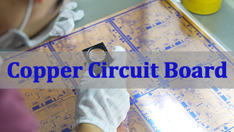
What Is A Copper Circuit Board And Why Is Copper Used In PCB Manufacturing?
A copper circuit board, at its core, is a non-conductive substrate laminated with a layer of copper foil, which is then patterned to create electrical pathways. Copper is the universal choice for the conductive layer in a printed circuit board due to its exceptional combination of properties, which are vital for medical electronics.
Why Copper is Indispensable:
- Superior Electrical Conductivity: Copper offers the highest conductivity among non-precious metals, ensuring minimal signal loss and power dissipation, crucial for sensitive medical sensors and signal processors.
- Excellent Thermal Conductivity: It efficiently transfers heat away from active components (like ICs and power regulators), enhancing device longevity and reliability.
- Strong Solderability: Copper forms reliable, strong solder joints, which is fundamental for the assembly and long-term stability of the copper pad for circuit board connections.
- Manufacturing Maturity: Processes for etching copper circuit boards, copper plating circuit boards, and bonding are well-established, allowing for high precision and yield.
In summary, the use of copper is foundational to PCB technology, providing the essential electrical and thermal performance required for dependable medical devices.
How Does Printed Circuit Board Copper Thickness Affect Current Carrying And Heat Dissipation?
Printed circuit board copper thickness is a foundational design variable that directly influences current capacity, thermal behavior, and long-term reliability. In medical electronics, where failure margins are minimal and compliance is mandatory, copper thickness selection must be deliberate and well justified.
At a physical level, copper thickness affects three critical performance dimensions:
- Current Capacity – Thicker copper supports higher ampacity at a given trace width, reducing the risk of localized overheating or trace degradation under load.
- Thermal Performance – Increased copper mass improves heat spreading, allowing hot spots to dissipate energy more evenly across the board structure.
- Electrical Resistance – Greater thickness lowers DC resistance, minimizing I²R losses and voltage drop along power distribution paths.
Industry standards such as IPC-2152 are commonly used to correlate copper weight, trace geometry, and allowable temperature rise in controlled environments.
Common PCB Copper Weights And Their Design Implications
| Copper Weight (oz/ft²) | Finished Thickness (mil / μm) | Primary Design Impact |
|---|---|---|
| 1 oz | 1.4 mil / 35 μm | Signal routing, low-current circuits |
| 2 oz | 2.8 mil / 70 μm | Power distribution, improved thermal margin |
| 3–4 oz | 4.2–5.6 mil / 105–140 μm | High-current paths, enhanced heat spreading |
| Heavy Copper (≥6 oz) | ≥8.4 mil / ≥210 μm | Extreme current and thermal management |
The table is intended for fast comparison; detailed electrical and thermal justification should always be verified through calculation and simulation.
Medical PCB Design Considerations
In medical device applications, copper thickness selection is rarely driven by electrical demand alone. Designers must also account for:
- Thermal safety limits imposed by patient-contact or enclosed device housings
- Mechanical constraints in compact or multilayer stack-ups
- Manufacturing consistency required for traceability and regulatory audits
Balancing these factors ensures that the selected printed circuit board copper thickness supports safe operation, predictable performance, and long-term reliability throughout the product lifecycle.
What Does 2oz Copper Thickness Mean In High-Power Circuit Board Design?
In high-power circuit board design, specifying 2 oz copper thickness is a strategic decision to enhance performance and reliability. The term “2 oz” means that two ounces of copper are spread over one square foot of area, resulting in a finished thickness of approximately 2.8 mils (70 microns).
For medical devices with high-power sections, 2 oz copper circuit board areas offer significant advantages:
- Higher Current Capacity: It can carry roughly twice the current of a standard 1 oz copper circuit board trace of the same width, allowing for narrower power traces or safer margins.
- Improved Thermal Management: The additional copper mass provides a lower thermal resistance path, helping to dissipate heat from high-power components like linear regulators or LED drivers in surgical lighting.
- Enhanced Mechanical Strength: Thicker copper traces circuit board layers add rigidity to the PCB and provide more robust anchor points for through-hole components, which is beneficial for connectors frequently engaged in medical settings.
- Reduced Voltage Drop: Lower DC resistance in power distribution networks ensures stable voltage delivery to critical components, such as sensors or amplifiers.
Therefore, using 2 oz copper thickness is a common and effective strategy to address the intertwined challenges of power delivery and heat in the demanding environments of medical electronics.
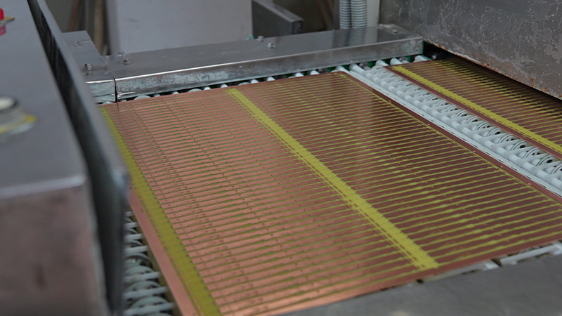
How to Make a Copper Clad Circuit Board?
The journey of creating a copper clad circuit board begins with the base material. Understanding this process highlights the importance of material quality for medical-grade reliability.
Core Manufacturing Steps:
- Substrate Preparation: A dielectric substrate (like FR-4, ceramic, or polyimide) is cleaned and prepared.
- Cladding: A thin layer of adhesive is applied, and a sheet of copper foil circuit board material is laminated onto the substrate under high heat and pressure. This creates the raw copper clad laminate circuit boards.
- For Double-Sided Boards: The process laminates copper foil onto both sides of the substrate, creating a double sided copper clad circuit board.
The quality of the raw copper clad printed circuit board material—its dimensional stability, dielectric properties, and copper peel strength—is foundational. For medical devices, using high-Tg FR-4 or other reliable FR4 copper clad laminate PCB printed circuit board material from trusted suppliers is essential to ensure performance under sterilization cycles and long-term use.
How Are Copper Traces Circuit Board Patterns Formed Through Etching Processes?
The intricate copper paths on circuit board are defined through a subtractive process called etching. This is a precision operation where unwanted copper is chemically removed, leaving behind the desired circuit pattern.
The Etching Process Flow:
- Lamination: A photosensitive dry film resist is laminated onto the clean copper clad circuit board.
- Imaging: The board is exposed to UV light through a photomask (film or LDI) containing the circuit pattern. The exposed areas of the resist harden.
- Development: The unexposed, soft resist is washed away, revealing the copper that needs to be removed.
- Etching: The board is immersed in a chemical etchant (e.g., alkaline ammonia). It dissolves the exposed copper, while the hardened resist protects the desired circuit board copper traces.
- Stripping: The remaining photoresist is stripped off, revealing the final copper traces circuit board pattern.
Precise control over copper circuit board etching is critical. Over-etching can cause trace narrowing, while under-etching can lead to shorts. For fine-pitch components common in medical electronics, this process must be executed with extreme accuracy to ensure signal integrity and reliability.
What Materials Circuit Board Structures Support Reliable Copper Bonding?
The long-term reliability of a copper plated circuit board depends on the materials that support and insulate the copper. The bond between copper and the substrate must withstand thermal stress, mechanical shock, and chemical exposure.
Key Material Considerations:
- Copper Foil: The type (electrodeposited ED or rolled-annealed RA) affects roughness and flexibility, influencing bond strength and high-frequency performance.
- Dielectric Substrate:
- FR-4 Epoxy Laminate: The most common. High-Tg FR-4 is preferred for medical devices for better thermal and chemical resistance.
- Polyimide: Used for flexible circuits, offering excellent heat resistance for applications like wearable monitors.
- Ceramic: Provides superior thermal conductivity for extreme heat dissipation.
- Adhesive System: The prepreg or bonding layer must have compatible thermal expansion coefficients and strong adhesion to prevent delamination.
The choice of copper circuit board material directly impacts the device’s ability to endure repeated sterilization, thermal cycling from operation, and mechanical stress, making it a cornerstone of medical printed circuit board reliability.
What Is Heavy Copper Printed Circuit Board Manufacturing And When Is It Required?
Heavy copper printed circuit board manufacturing refers to processes that create boards with copper weights significantly above 3 oz, often ranging from 6 oz to 20 oz or more per layer. This is not just about thick foil; it involves specialized plating and etching techniques.
When is a Heavy Copper PCB Required?
- Extreme High Current: Devices like defibrillator charging circuits, X-ray generator controls, or surgical robot power drives.
- Enhanced Thermal Management: Acting as an integrated heat spreader in power-dense assemblies where external heatsinks are not feasible.
- High Reliability Interconnects: Where the copper strip circuit board pathways must withstand repeated high-energy pulses without degradation.
- Harsh Environments: Providing extra material to tolerate higher levels of vibration or thermal cycling.
EBest Circuit (Best Technology) is committed to manufacturing high-quality heavy copper PCBs and providing reliable PCB assembly services. The heavy copper printed circuit board manufacturing process often uses a combination of thick-core lamination and step-plating to build up the copper in defined areas, allowing for a mix of fine-pitch signal traces and massive power planes on the same layer.
How To Clean And Maintain Copper Printed Circuit Board Surfaces Over Time?
Protecting the exposed copper traces on a circuit board is vital to prevent oxidation (“tarnishing”) which can degrade solderability and cause intermittent connections. For medical devices, this is part of ensuring long-term field reliability.
Best Practices for Copper Surface Preservation:
- Surface Finish: Apply a protective coating immediately after fabrication. Common medical-grade finishes include:
- ENIG (Electroless Nickel Immersion Gold): Excellent for fine-pitch components and wire bonding. Provides a flat, oxidation-resistant surface.
- Immersion Silver/Tin: Good solderability and a cost-effective alternative.
- OSP (Organic Solderability Preservative): A thin, organic layer that protects copper until soldering.
- Proper Storage: Store PCBs in a moisture-barrier bag with desiccant in a temperature and humidity-controlled environment.
- Handling: Always wear gloves to prevent contamination from skin oils and salts.
- Cleaning: If cleaning is necessary, use medical-grade, residue-free fluxes and cleaners compatible with the surface finish to avoid damage.
Implementing these steps ensures the copper printed circuit board surfaces remain pristine from the copper circuit board factory through assembly and throughout the device’s operational life.
Why Choose Best Technology as Your Reliable China Copper Circuit Board Factory?
Selecting the right manufacturing partner is the most critical decision in bringing a medical device to market. EBest Circuit (Best Technology) stands out as a premier China copper circuit board factory for medical applications.
Our Core Advantages:
- Medical-Grade Focus: We are certified to ISO 13485, understanding the documentation, traceability, and risk management requirements of the medical industry.
- Advanced Technical Capability: From standard FR4 copper clad circuit board to complex heavy copper and HDI designs, our engineering team can support your most challenging requirements.
- Rigorous Quality System: Our process control, from incoming copper clad laminate PCB inspection to final electrical testing, ensures consistent, high-yield production.
- Supply Chain Stability: As an established manufacturer, we have strong relationships with material suppliers, guaranteeing access to high-quality, certified raw materials.
- Responsive Service: We act as an extension of your team, providing clear communication, rapid prototyping, and reliable production scheduling.
Pls feel free to contact us anytime at sales@bestpcbs.com to discuss how we can manufacture the certified, reliable copper circuit boards your medical device deserves.
In a nutshell, copper circuit boards are the vital, conductive heart of every advanced medical device, enabling precision, power, and communication. This article has explored the critical aspects—from material science and circuit board copper thickness to certified manufacturing printed circuit processes—that ensure these boards meet the life-critical standards of the medical field.
Navigating the complexities of copper circuit board manufacturing process for certified medical devices demands a partner with specialized expertise, robust quality systems, and a deep understanding of regulatory landscapes. EBest Circuit (Best Technology) is committed to being that partner, providing the reliability, performance, and compliance your innovations require. For technical or project-related inquiries, please contact us at sales@bestpcbs.com.
FAQs
What Are The Copper Lines On A Circuit Board Called?
The copper lines on a circuit board are called traces (or tracks). They form the conductive pathways that electrically connect components. The pattern of copper traces circuit board is defined during the etching process.
What Is I-L Copper Length For Printed Circuit Boards?
“I-L copper length” is not a standard industry term. It is likely a misinterpretation. You may be referring to:
- Trace Length: Critical for timing in high-speed digital circuits (like in imaging data buses).
- Annular Ring: The width of the copper pad for circuit board around a drilled hole.
- IPC Specs: Standards like IPC-4552 for ENIG or IPC-6012 for performance qualification. For clarification on specific requirements, please consult your manufacturer’s engineering team.
What Is The Standard Copper Spec For A Circuit Board?
There is no single “standard” spec, as it depends on the board’s function. The most common base weight is 1 oz copper (≈35μm thick). However, specifications are defined in the fabrication drawing and typically include:
- Copper Weight: e.g., 1 oz, 2 oz for inner/outer layers.
- Final Finished Thickness: After plating and processing.
- IPC Class: Class 2 (general electronics) or Class 3 (high reliability, which includes medical devices).
- Surface Finish Type: e.g., ENIG, Immersion Sn.