

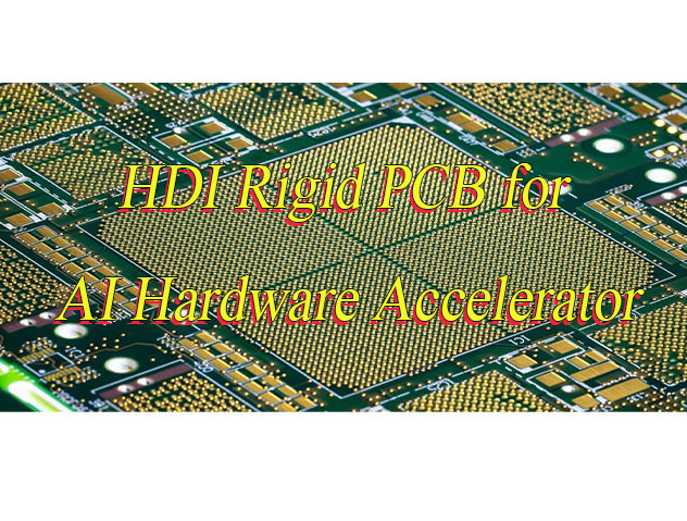
Why choose HDI rigid PCB for AI hardware accelerator? Let’s discover benefits, applications, power integrity design, thermal solution, cost-performance balancing strategies for HDI rigid PCB for AI accelerator.
Are you troubled with these problems?
- How can high-frequency signal transmission in AI acceleration hardware avoid interference loss?
- How does high-density HDI wiring solve heat dissipation challenges?
- How can complex HDI designs shorten production cycles?
As a HDI Rigid PCB Manufacturer, EBest Circuit (Best Technology) can provide you service and solutions:
- Lossless signal transmission: ≤50μm line width/space + 6-layer blind and buried vias reduce signal loss by 30%, ensuring uncompromised computing power in high-frequency scenarios.
- 3D heat dissipation architecture: A combination of thermal channels, metal base, and heat dissipation vias supports stable operation with a heat flux density of ≥5W/cm².
- Rapid mass production delivery: 48-hour rapid prototyping + 7-day mass production, with full process visualization, shortening AI hardware time-to-market.
Welcome to contact us if you have any request for rigid HDI PCB: sales@bestpcbs.com.
Why is HDI Rigid PCB Important for AI Hardware Accelerator?
Benefits of HDI Rigid PCB in AI Hardware Accelerator:
- High-Density Routing & Micro-Via Technology: HDI PCBs achieve high-density routing through microvias (diameter ≤0.006 inches), blind/buried vias, and ultra-fine traces (<3 mils), reducing signal path length and latency. For example, in Transformer-based AI chips, data transmission latency decreases from 1ns to 0.7ns, with routing density increasing 5-fold.
- Signal Integrity Optimization: Low-Dk/Df materials (e.g., M7, Rogers 4350B) combined with differential signal design ensure 10GHz signal insertion loss of only 0.5dB. Eye diagram opening improves by 20%, with bit error rates as low as 1e-15, meeting PCIe 5.0 specifications.
- Thermal Management: Ultra-thin 0.1mm substrates paired with high-thermal-conductivity resins (1W/m·K) and nickel-gold plating (90W/m·K) shorten heat dissipation paths by 40%. This reduces junction temperature by 10°C, lowers fan speeds by 20%, and decreases noise by 5dB.
- Manufacturing Precision: UV laser drilling achieves ≤3μm positioning accuracy, while X-ray alignment systems control lamination deviations <5μm. Layer-to-layer connectivity reaches 99.99%, and pad flatness is maintained below 1μm, ensuring robust connections for high-reliability applications.
- Cost Efficiency & Long-Term Value: Despite higher upfront costs, HDI’s integration density reduces power waste and enhances efficiency. For AI servers, HDI PCB value increases from $500 to $2,500, with margins improving by 15–20 percentage points. Total Cost of Ownership (TCO) decreases over the product lifecycle.
- High-Speed Interface & High-Frequency Support: Low-Dk/Df substrates (e.g., Megtron 8, Tachyon 100G) minimize signal loss and improve electromagnetic compatibility for high-speed digital interfaces, enabling seamless integration with PCIe 5.0 and beyond.
- Miniaturization & High Reliability: HDI’s compact form factor suits constrained devices like 5G base stations and smartphones, while withstanding harsh environments (-40°C to 125°C) for automotive and aerospace applications.
- Advanced Manufacturing Innovations: Laser drilling, sequential lamination, and automated optical inspection (AOI) ensure precision for advanced HDI stages (e.g., ≥4-layer), supporting future technologies like 3D ICs and chiplet-based designs.
Applications of Rigid HDI PCB in AI Hardware Accelerator
Applications of AI accelerator rigid HDI PCB:
- AI Server GPU Accelerator Cards
- Edge AI Accelerators
- Autonomous Driving Platforms
- Data Center Compute Modules
- 5G Base Station Acceleration Modules
- Aerospace Computing Units
- Smart Security Cameras
Signal Integrity Optimization in HDI Rigid PCB for High Frequency AI Accelerator
Precise Impedance Control
- For critical signal lines (e.g., clocks, data buses) in HDI rigid PCBs for high-frequency AI accelerators, use TDR (Time-Domain Reflectometry) simulation and real-world measurements to ensure single-ended line impedance is strictly controlled at 50±5Ω and differential pair impedance at 100±10Ω. Prevent signal reflection exceeding 3% due to impedance mismatch.
- During layer stack design with tools like Polar SI9000, specify parameters such as substrate thickness, copper foil thickness (≥18μm), dielectric layer Dk/Df values (e.g., Megtron 6: Dk=3.9±0.05), and prioritize embedded capacitance/inductance technologies to minimize via counts.
Crosstalk Suppression Strategy
- Apply the “3W rule” (trace spacing ≥3× trace width) for high-speed signal lines. Maintain differential pair inner spacing within 2× trace width and adjacent signal spacing ≥5× trace width.
- Deploy isolated ground planes in critical areas (e.g., around CPUs) and add grounding vias (spacing ≤200mil) to form Faraday cages, limiting crosstalk noise to ≤5% of signal amplitude. For signals above 10GHz, use shielded differential pairs (e.g., trace structures with ground shields).
Power Integrity Optimization
- Adopt a “power plane + decoupling capacitor” dual approach. Segment the main power plane into independent regions (e.g., AI chip core voltage 1.2V, I/O voltage 3.3V) and connect via ≥50mil/200mil via arrays.
- Place decoupling capacitors following the “proximity principle”: 0.1μF/0.01μF capacitor combinations ≤5mm from chip pins. Use tools like Ansys SIWave for PDN (Power Distribution Network) analysis to determine capacitor quantities and values, ensuring power noise ≤2% voltage ripple.
Precision Layout and Routing
- Follow “short and straight” principles for critical signal paths, avoid 90° bends (use 45° chamfers or arc transitions) and minimize via counts (≤2 vias per trace).
- For BGA packages, use “dog-bone routing” with blind/buried via technologies (e.g., HDI 2nd-order vias) to achieve smooth transitions from chip pins to PCB outer layers. Implement length matching (error ≤50mil) and use serpentine routing for timing adjustment.
Material and Process Selection
- Prioritize low-loss substrates (e.g., Panasonic Megtron 7: Df≤0.002) with thin dielectric layers (≤3mil) to reduce signal delay.
- For surface finishes, use ENIG (Electroless Nickel Immersion Gold) or OSP (Organic Solderability Preservative) to avoid HASL (Hot Air Solder Leveling)-induced surface roughness increasing signal loss.
- For microvia filling, adopt high-reliability electroplating processes to ensure void-free via interiors and IST (Interconnect Stress Test) certification for reliability.
Efficient Power Integrity Design in HDI Rigid PCB for AI Accelerators
1. Refined Modeling of Power Distribution Network (PDN)
- Implementation Steps: Utilize 3D electromagnetic simulation tools (e.g., Ansys HFSS/SIwave) to construct a PDN model, focusing on simulating impedance characteristics at AI chip power pins. Target impedance should be controlled within 2%-5% of the target voltage (e.g., ≤20mΩ for 1V power supply).
- Critical Parameters: Determine via simulation the impact of power plane thickness (≥1oz recommended), dielectric layer thickness (≤0.1mm for HDI boards), and via dimensions (blind via diameter ≤0.2mm) on impedance.
- Validation Method: Measure impedance at key nodes using a network analyzer to ensure deviation from simulation results is <5%.
2. Hierarchical Layout Strategy for Decoupling Capacitors
- Near-Chip Layer: Deploy 0.1μF–10μF high-frequency decoupling capacitors (X7R material) within a 5mm radius of AI chip power pins, adhering to the “minimized loop area” wiring principle.
- Intermediate Layer: Insert a 0.01μF–0.1μF capacitor layer between power and ground planes to form a “capacitor-plane sandwich” structure, reducing inter-plane resonance frequency.
- Bottom Layer: Place large-capacity (≥100μF) low-frequency decoupling capacitors, using multiple parallel vias to minimize ESL (equivalent series inductance).
- Execution Standard: Conduct PDN impedance scanning post-layout to ensure resonance peaks do not exceed 50Ω within the target frequency band (e.g., <1GHz).
3. Collaborative Segmentation Design for Multi-Power Domains
- Segmentation Principles: Divide power planes into “island” segments based on AI accelerator voltage domains (e.g., core 1.2V, I/O 3.3V), with adjacent domains spaced ≥2mm apart and separated by ≥20mil-wide ground plane isolation strips.
- Via Bridging: Implement “cross-segment capacitor bridging” by placing 2–4 0.01μF capacitors along segment boundaries to reduce cross-segment noise.
- Simulation Verification: Validate signal integrity across segmentation boundaries via SI/PI co-simulation, ensuring crosstalk <5% of signal amplitude.
4. HDI Microvia Power Plane Optimization
- Blind/Buried Via Design: Use a hybrid “blind via + buried via” structure for interlayer power connections, minimizing via-induced plane segmentation. Recommended blind via diameter: 0.15–0.2mm, aspect ratio ≤1:6.
- Microvia Filling: Electroplate copper-filled microvias on high-frequency current paths to reduce via resistance (target ≤0.5mΩ).
- Thermal Via Design: Add thermal via arrays (spacing ≤1mm, diameter 0.3mm) beneath high-heat regions (e.g., under chips) to connect to bottom-layer thermal layers.
5. Dynamic Power Noise Suppression System
- Real-Time Monitoring: Integrate voltage sensors at AI chip power pins, using FPGA or dedicated chips for real-time voltage fluctuation monitoring.
- Dynamic Compensation: Adjust decoupling capacitor array switching states or dynamically regulate supply voltage via LDO regulators (accuracy ±1%) based on monitoring data.
- Execution Case: Validate the dynamic compensation system on test boards to ensure voltage fluctuations <2% during load step changes (e.g., 1A/μs).
6. Material and Process Selection Specifications
- Substrate Selection: Use low-loss HDI substrates (e.g., Panasonic M7N) with dielectric constant ≤4.5 and loss tangent ≤0.005.
- Surface Treatment: Apply ENIG (electroless nickel gold) to power planes for low contact resistance; use OSP (organic solderability preservative) on ground planes for reliable conduction.
- Manufacturing Control: Maintain layer-to-layer alignment accuracy ≤±50μm during HDI board lamination to ensure microvia alignment with pads.
7. Thermal Management and Heat Dissipation Co-Design
- Thermal Layer Layout: Deploy a ≥2oz copper thermal layer at the PCB bottom, connected via thermal vias (diameter 0.5mm, spacing 5mm) to power planes under chips.
- Thermal Simulation Verification: Use thermal simulation tools (e.g., FloTHERM) to analyze heat dissipation paths, ensuring chip junction temperature <105°C at 40°C ambient.
- Practical Testing: Perform infrared thermal imaging tests on prototypes to validate thermal path effectiveness.
8. Standardized Verification and Debugging Process
- Simulation Phase: Complete PDN impedance, signal integrity, and thermal simulation validations; generate and archive simulation reports.
- Testing Phase: Measure power noise (bandwidth ≥1GHz) using oscilloscopes to ensure peak-to-peak noise <50mV; scan EMI emissions with near-field probes to comply with FCC Class B standards.
- Debugging Phase: Iteratively optimize issues identified during testing (e.g., adjust decoupling capacitor positions, add thermal vias) until all design requirements are met.
Thermal Management Solutions for HDI Rigid PCB in AI Accelerator
- High Thermal Conductivity Material Application: Utilize ceramic-filled epoxy substrates, aluminum-based composites, or metal-core materials (e.g., copper/aluminum) to achieve thermal conductivity of 5–10 W/(m·K). Integrate embedded copper heat blocks or graphene coatings to reduce thermal resistance between high-power chips (e.g., GPU/ASIC) and PCB, enabling efficient lateral heat diffusion in hotspots.
- Multi-layer Thermal Channel Construction: Implement 20+ layer stack-up designs with dedicated thermal layers embedded between high-speed signal and power layers. Leverage blind/buried via technology to form vertical thermal pathways, paired with thermal via arrays (0.3mm diameter, 1mm pitch) to efficiently transfer heat from 300–500W high-power devices to metal backplates or liquid cooling systems, reducing thermal resistance by over 40%.
- Layout Zoning & Airflow Optimization: Segment layout by power density, position high-power components (≥50W, e.g., GPU/ASIC) at PCB edges/top, and thermally sensitive devices at cold air inlets. Optimize airflow paths via CFD simulation to prevent local hotspots and enhance convective cooling efficiency, ensuring unobstructed airflow paths.
- Active Cooling System Integration: Deploy microchannel cold plates directly bonded to high-power chips with fluorinated fluid cooling for 130W/cm² heat flux dissipation. Immersion cooling enhances thermal conductivity by 10× for ultra-high-performance AI clusters. Integrate backside mini-fan arrays and heat pipes with PWM-controlled speed regulation to balance cooling and noise, maintaining operating temperatures ≤85°C.
- Thermal Simulation & Reliability Validation: Use ANSYS Icepak or equivalent tools for thermal modeling to predict hotspot distribution and optimize layouts. Validate solder joint reliability via accelerated thermal cycling (-40°C to 125°C) and monitor thermal distribution in real-time via infrared thermography for stable AI inference operations.
- EMI Shielding & Safety Protection: Maintain ≥2mm clearance between cooling structures and high-speed traces (e.g., PCIe 5.0/DDR5) to avoid EMI. Use dielectric coolants (e.g., 3M Novec) to prevent electrical shorts. Incorporate temperature sensors and over-temperature protection circuits for automatic throttling or cooling mode switching during faults.
- Advanced Process & Material Innovation: Employ HDI microvia technology (≤0.1mm diameter) to enhance routing density. Adopt high-Tg substrates (Tg ≥170°C) for thermal stability. Apply phase-change materials or thermal interface materials (e.g., thermal grease) on PCB surfaces to reduce interfacial thermal resistance and improve overall cooling efficiency.
Cost-Performance Balancing Strategies for HDI Rigid PCB in AI Accelerators
Material Selection & Cost Optimization
- Prioritize low Dk/Df materials (e.g., MEGTRON 6, Rogers 4350B) to reduce dielectric loss by 25% for ≥10Gbps signal integrity. Reduce copper thickness from 2oz to 1oz to cut material costs by 23% for modules with current density ≤1A/mm². Standardize board thickness to 1.6mm to lower processing costs by 15% and enhance batch production efficiency.
Symmetrical Stackup Design
- Adopt an 8-layer symmetrical “signal-ground-power-signal” stackup with alternating power/ground planes to balance CTE and minimize warpage. Maintain signal-layer to reference-plane coupling distance within ±0.05mm to reduce crosstalk by 15%.
High-Speed Signal Path Optimization
- Implement strict impedance control (85Ω/100Ω) for differential pairs with equal-length serpentine routing (≤5mil error) for PCIe 5.0/6.0 signals. Use backdrilling to eliminate via stubs and reduce reflections. For HBM-AI chip interconnections, adopt TSV short-path design to limit latency to ≤50ps.
Power Integrity (PI) Enhancement
- Deploy multi-layer power/ground plane stackups with zoned power islands for Vcore/Vmem rails. Place 0201-sized high-frequency decoupling capacitors (100nF+10nF) beneath BGA packages, paired with low-ESL/ESR capacitors to suppress power noise to ≤5mV.
Thermal Co-Design
- Integrate high-thermal-conductivity substrates (>5W/m·K) with copper heat sinks and thermal via arrays to form 3D heat dissipation channels. For >300W AI core areas, embed liquid-cooling plates with TIM materials to boost thermal conductivity by 40%. Optimize thermal paths via simulation to eliminate hotspots.
Manufacturing Cost Control
- Maximize material utilization to >90% through panelization. Balance test coverage and cost by setting test point density to 0.8/cm². Enlarge solder mask openings by 0.1mm to improve soldering yield by 5% and reduce rework costs.
HDI Structure Selection
- Evaluate cost increments (40%-200%) for Type I/II/III HDI structures, prioritizing Type II for cost-performance balance. Avoid ≤0.3mm special via designs; use laser microvia technology (3mil/3mil line/space) for high-density routing.
Power Path Optimization
- Utilize ≥100mil wide copper traces for key power paths to limit current density to ≤3A/mm². Deploy ≥6 parallel vias to reduce power loop inductance and enhance current capacity. Position VRM modules near high-power regions to shorten power paths.
AI-Driven Design Tools
- Leverage AI algorithms for component placement (e.g., UCIe Chiplet modules) to minimize EMI and shorten signal paths by 20%. Use AI-based autorouting to reduce via count by 15% and lower crosstalk. Implement AI defect detection for early fault warning to prevent production losses.
DFM Integration
- Incorporate DFM validation during design to assess manufacturability parameters (line/space, via size, layer alignment). Ensure layer precision via AOI/X-Ray inspection to minimize rework. Collaborate with suppliers for material/process optimization and long-term cost reduction.
Why Choose EBest Circuit (Best Technology) as HDI Rigid PCB Manufacturer?
Reasons why choose us as HDI rigid PCB manufacturer:
- Competitive Pricing with Value Optimization: Leveraging dynamic cost modeling and bulk procurement advantages, we offer 8%-15% lower quotes than industry averages. Combined with tailored design optimization, we help reduce material costs by over 20% during the design phase, delivering both cost efficiency and technical excellence.
- 24-Hour Rapid Prototyping for Market Leadership: Our dedicated express channel delivers prototypes from design confirmation to sample in just 24 hours—60% faster than standard lead times. This accelerates product iteration and ensures you capture critical market windows without delay.
- 99.2% On-Time Delivery: Powered by intelligent ERP systems and flexible capacity allocation, we achieve a 99.2% on-time delivery rate, far exceeding industry benchmarks. This minimizes production delays, reduces inventory risks, and safeguards your supply chain stability.
- Strict Quality Control System: Triple-layer inspection (AOI + AI visual review + manual final check) ensures 100% batch inspection with defect rates below 0.03%. This exceeds industry standards, enhancing product reliability and reducing post-sale costs.
- Global Compliance with Premier Certifications:Certified with ISO 9001, ISO 13485 (medical), IATF 16949 (automotive), and RoHS, we meet stringent global market requirements. This facilitates seamless entry into regulated markets like EU, North America, and beyond.
- 19-Year Process Database for Risk Mitigation: Backed by 19 years of manufacturing data and a million-case error library, our intelligent alarm system predicts 98% of potential process risks. This reduces trial production rework and cuts hidden costs by over 30%.
- Free DFM Analysis for Design Excellence: Complimentary Design for Manufacturability (DFM) reviews cover 20+ critical dimensions—including trace width/spacing, impedance matching, and testability. This preempts 90% of manufacturing risks and shortens time-to-market by 2-4 weeks.
- End-to-End One-Stop Solutions: From design consultation and engineering validation to mass production and global logistics, we provide a single-window service. This reduces supply chain coordination costs by over 30% and simplifies project management.
Welcome to contact us if you have any inquiry for rigid HDI PCB: sales@bestpcbs.com.