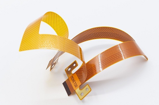
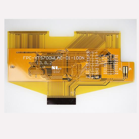
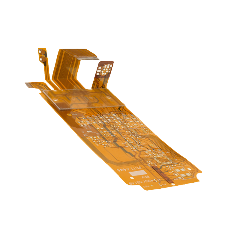
Looking for flex circuit fabrication manufacturers in Oregon? This blog includes selection guide and manufacturer list for Oregon flexible PCB manufacturers.
Are you troubled with these problems?
- How to quickly respond to prototype requirements given the frequent iterations of flexible circuit design?
- How to ensure signal integrity when interlayer alignment accuracy in multilayer flexible boards is insufficient?
- How to control impedance fluctuations and losses in high-frequency signal transmission scenarios?
As a flexible circuit board manufacturer, EBest Circuit (Best Technology) can provide you service and solution:
- Agile Development System: Provides 72-hour rapid prototyping service, supporting collaborative design-simulation-manufacturing processes to shorten product development cycles.
- High-Precision Lamination Technology: Employs a micron-level alignment system and laser drilling technology to ensure interlayer misalignment ≤ ±25μm, meeting the needs of complex signal transmission.
- Dynamic Impedance Management: Through optimized material selection and real-time calibration of linewidth/spacing, impedance fluctuations in high-frequency signal transmission are controlled within ±5%.
Feel free to contact us if you have any inquiry for flex circuit board: sales@bestpcbs.com.
Why Choose Flex Circuit Fabrication Manufacturer in Oregon?
Advantages of Flex Circuit Fabrication Manufacturer in Oregon:
- Cutting-edge technology ensures innovation implementation: US manufacturers possess advanced technologies such as 15/15µm ultra-fine lines and 3D packaging, suitable for high-precision applications in medical, aerospace, and consumer electronics, helping to overcome traditional wiring limitations.
- Stringent quality control reduces failure risk: Adhering to international standards such as IPC/MIL, using high-temperature resistant polyimide substrates and highly stable electroplated copper foil ensures circuit reliability in extreme environments, reducing subsequent maintenance costs.
- Local supply chain accelerates product launch: Localized production shortens transportation cycles, and coupled with a rapid response team, efficient collaboration throughout the entire process from design consultation to mass production shortens the development cycle by more than 30%.
- Environmental compliance aligns with global trends: Strictly adhering to environmental regulations such as RoHS, using recyclable materials and low-carbon processes, meeting the green manufacturing requirements of markets such as North America and Europe, and avoiding compliance risks.
- Strong intellectual property protection prevents plagiarism: Dual protection by US patent law and the Convention on the Intellectual Property Rights of Integrated Circuits clearly defines the boundaries of reverse engineering, effectively protecting designers’ innovative achievements and trade secrets.

Flex Circuit Fabrication Manufacturers in Oregon
Custom Contract Manufacturing (CCM)
Main Business:
- Focuses on prototyping and contract manufacturing of flexible printed circuit boards (Flex PCBs), covering the entire process from concept design to functional prototypes.
Advantages include:
- Rapid prototyping delivery capabilities, enabling rapid production of high-precision prototypes based on customer designs, effectively shortening product verification cycles;
- Providing end-to-end quality control, covering the entire process from design evaluation and process optimization to finished product testing;
- Offering customized solutions for concept testing, durability verification, and layout optimization needs, helping customers perfect their designs before mass production.
ASC Sunstone Circuits
Main Business:
- Covers the manufacturing of high-performance PCBs, including flexible and rigid-flex PCBs, serving multiple industries such as industrial, aerospace, and defense.
Advantages include:
- Mastery of advanced process technologies such as High-Definition Interconnect (HDI), metal substrates, RF/microwave, and flexible/rigid-flex;
- Comprehensive certifications, including key industry certifications such as IPC-6012 Class II/III, UL 976 (flame retardant), and ITAR (Defense Trade Controls);
- A robust customer support system, providing 24/7/365 on-site technical support, an on-time delivery rate exceeding 99%, and free PCB123® CAD design software to significantly improve design efficiency.
MaRCTech2, Inc.
Main Business:
- Design, manufacturing, and delivery of flexible and rigid-flex PCBs, supporting high-density interconnects (HDI) from single-layer to arbitrary-layer, as well as complex processes such as blind vias, buried vias, and via-in-pads.
Advantages include:
- A rich diversity of materials and processes, utilizing a variety of high-performance materials such as heavy copper, aluminum-based materials, IMS, and Rogers, and offering a full range of surface treatment options;
- Rapid delivery capabilities, providing 24-hour expedited service and 30:1 aspect ratio micro-hole machining, suitable for rapid prototyping and small-batch projects;
- End-to-end capabilities across the entire chain from conceptual design and DFM to mass production, and AS9100D and ITAR certified, meeting the high reliability requirements of aerospace, medical, and other fields.
How to Select A Oregon Flex Circuit Fabrication Manufacturer?
A Practical Selection Guide to Oregon Flex Circuit Fabrication Manufacturer:
1. Technical Capability Alignment and Verification
- Identify project requirements such as high-frequency high-speed materials, thick copper, or rigid-flex combinations.
- Verify the manufacturer’s support for materials like PI substrates (high-temperature resistance) or LCP (low dielectric loss). Confirm dynamic bending test capabilities, including bend radius and cycle life, through technical documentation or audits.
2. Quality Certification and Industry Compliance
- Match mandatory certifications to target markets: IATF 16949 for automotive, ISO 13485 for medical devices, AS9100 for aerospace.
- Ensure test reports align with standards like IPC-2223 (bend radius ≥10x FPC thickness) and environmental testing capabilities (-40°C to 85°C cycle testing).
3. Delivery Reliability and Supply Chain Resilience
- For small-batch prototyping, prioritize agile manufacturers with rapid sampling (e.g., 24-hour turnaround).
- For mass production, select globally distributed manufacturers to mitigate single-point risks. Evaluate multi-site production networks to support cross-border logistics and continuity.
4. Cost Efficiency and Transparent Pricing
- Compare pricing models across small and large orders, factoring in MOQ, unit costs, and scale-related premiums.
- Analyze total landed costs, including transportation and tariffs. Avoid hidden fees by clarifying inclusion of technical support, maintenance, and post-sale services.
5. Cross-Border Collaboration Experience
- Prioritize manufacturers with proven international project experience, such as serving global tech firms.
- Ensure multilingual communication support, real-time collaboration tools, and 24/7 technical response systems to streamline cross-regional teamwork.
6. Environmental Compliance and Sustainability
- Validate adherence to regulations like RoHS and REACH. Confirm use of recyclable materials and low-carbon production processes.
- Check compliance with Oregon’s EPR laws and participation in circular economy initiatives to meet global sustainability benchmarks.
7. Post-Sale Support and Long-Term Partnership
- Evaluate response times for technical support, repair cycles, and spare parts availability.
- Select manufacturers offering end-to-end services (R&D to after-sales) to prevent project delays or cost overruns. Ensure long-term technical advisory and maintenance programs are available.

Flex Circuit Board Fabrication Process
1. Cutting: Cut large rolls of polyimide (PI) or polyester (PET) substrate into individual sheets of the specified size. High-precision cutting equipment must be used to ensure dimensional tolerances ≤ ±0.1mm.
2. Baking: Place the cut substrate in an oven and bake at 120-150℃ for 2-4 hours to remove internal moisture and stress, improving dimensional stability.
3. Drilling: Use a CNC drilling machine to drill through holes or blind holes in the substrate. The hole diameter accuracy must be controlled within ±0.05mm, and the hole walls must be smooth and burr-free.
4. Copper Plating: Form a conductive layer on the hole walls through chemical copper plating or black hole processes, followed by electroplating to thicken the copper layer to 5-20μm, ensuring reliable interlayer electrical connections.
5. Brushing: Use a brushing machine to remove the oxide layer and contaminants from the substrate surface, improving dry film adhesion.
6. Dry Film Lamination: Apply photosensitive dry film to the substrate surface. Lamination pressure and temperature must be controlled to avoid bubbles or wrinkles.
7. Alignment and Exposure: Use a CCD alignment system to precisely align the film or LDI with the substrate. After UV light irradiation, the dry film undergoes a polymerization reaction to form the circuit pattern.
8. Developing: Dissolve the unexposed dry film with an alkaline solution to expose the copper layer areas to be etched.
9. Etching: Use an acidic etching solution (such as copper chloride) to etch away the exposed copper layer, preserving the circuit pattern protected by the dry film.
10. Circuit Quality Check: Inspect the circuit width, spacing, hole position deviation, and for defects such as short circuits/open circuits using AOI automated optical inspection or manual visual inspection, and record the location and type of defects.
11. Polishing: Clean the circuit surface again to improve the adhesion of the cover film.
12. Applying Cover Film: Apply PI or PET cover film to the circuit surface to protect and insulate the circuit. Lamination pressure and temperature must be controlled to avoid bubbles.
13. Lamination: Use a high-speed press or vacuum press to laminate the cover film to the substrate. The pressure must be uniform to ensure no delamination.
14. Curing: Cure the laminated board in a high-temperature oven to ensure a tight bond between the cover film and the substrate, improving heat and chemical resistance.
15. Surface Treatment (Immersion Gold): Apply chemical immersion gold to the pads or connector areas to form a 2-5μm nickel-gold layer, improving soldering reliability and corrosion resistance.
16. QC (Secondary Inspection): Perform visual inspection (e.g., gold surface uniformity, no oxidation), electrical testing (e.g., conductivity, insulation), and reliability testing (e.g., thermal shock, salt spray testing) on the immersion gold-plated products.
17. Flying Probe Testing: Use a flying probe tester to perform 100% electrical testing on the circuit, detecting defects such as open circuits, short circuits, and abnormal impedance, and generate a test report.
18. PI Reinforcement: Apply PI reinforcing sheets to areas requiring reinforcement (e.g., connectors, pads) to improve mechanical strength.
19. Lamination: The reinforcing sheet is laminated to the substrate, ensuring no air bubbles or delamination.
20. Silk Screen Printing: Component identification, company logo, version numbers, and other characters are screen printed onto the substrate surface. Ink thickness and positional accuracy must be controlled.
21. Baking and Curing: The ink is cured by baking, improving the characters’ abrasion resistance and chemical resistance.
22. Laser Cutting: The product shape is cut according to the design contour using a laser cutting machine. Accuracy must be controlled within ±0.1mm, and edges must be smooth and burr-free.
23. FR4 Reinforcement: FR4 reinforcing plates are attached to areas requiring additional support to improve overall rigidity.
24. Final Quality Control (FQC): A comprehensive inspection of the finished product is conducted, including appearance, dimensions, electrical performance, and reliability, ensuring no defective products are shipped.
25. Final Quality Audit (FQA): The quality department conducts sampling audits to verify FQC results, ensuring product quality meets customer and industry standards.
26. Packaging: Antistatic packaging materials (such as antistatic bags and pearl cotton) are used to protect the product from damage during transportation.
27. Shipment: Manage warehousing according to order requirements and arrange logistics for shipment. Verify the shipment quantity and packaging labels to ensure accuracy.

Flex Circuit Board Fabrication Notes
Material Selection and Performance Matching:
- Polyimide (PI) is the core substrate material, with thickness options (12.5μm/25μm/50μm) selected based on application scenarios. High-Tg PI is preferred for high-temperature environments, while polyester (PET) can be considered for low-temperature or cost-sensitive scenarios.
- Substrate thickness directly affects bending radius—12.5μm PI supports a minimum bending radius of 0.1mm, suitable for wearable devices; 50μm PI is ideal for industrial-grade dynamic flexing scenarios.
- Ensure compatibility between substrate and adhesive to prevent delamination, ensuring reliability.
Circuit Design and Manufacturing Precision Control:
- Minimum line width/spacing must align with etching capabilities (conventional 0.08mm/0.08mm, high-precision 0.05mm/0.05mm). Dynamic flexing areas require serpentine routing and stress relief slots to avoid stress concentration-induced fractures.
- Pad design must account for coverlay windowing accuracy (±0.05mm) and surface treatments (ENIG/OSP). High-frequency signals require coplanar waveguide structures to minimize crosstalk.
- Multilayer boards utilize laser drilling for microvias (diameter starting at 0.15mm). Electroplating fill uniformity must be controlled to prevent voids, ensuring signal integrity.
Lamination Process and Stress Management:
- Multilayer flexible board lamination employs vacuum hot-pressing with precise temperature curve control (e.g., PI glass transition temperature ~360°C) to avoid substrate degradation.
- Interlayer adhesive thickness must be uniform (25-35μm) to prevent air bubbles causing short circuits. Dynamic areas adopt localized adhesive-free designs to reduce stress, while static areas use stiffeners (e.g., FR4) for enhanced support.
- Bending tests simulate real-world usage (e.g., 100,000+ cycles at 180° bending) to verify fatigue resistance and product longevity.
Coverlay and Solder Mask Application:
- Coverlay materials (PI or PET) must match the substrate, with windowing accuracy (±0.05mm) directly impacting pad reliability.
- Solder mask uses liquid photoimageable (LPI) process, with thickness controlled at 10-20μm to avoid impacting circuit accuracy. High-frequency applications require low-dielectric solder mask materials to reduce signal loss.
- Surface treatments balance solderability and environmental resistance—ENIG for fine-pitch pads, OSP for cost-sensitive scenarios.
Reliability Verification and Failure Analysis:
- Environmental testing includes thermal shock (-40°C~125°C for 1000 cycles) and salt spray (96h) to validate durability across harsh conditions.
- Failure analysis employs X-ray inspection for microvia voids, scanning electron microscopy (SEM) for fracture morphology, and high-speed cameras for crack propagation monitoring during dynamic flexing tests.
- Design includes test points for in-line inspection during manufacturing and post-sale diagnostics, ensuring traceability and rapid issue resolution.

Why Oregon Clients Trust EBest Circuit (Best Technology) for Flex Circuit Fabrication?
Reasons Why Choose EBest Circuit (Best Technology) as Flex Circuity Fabrication Manufacturer:
- Free DFM Design Optimization Analysis: Our expert team provides complimentary DFM (Design for Manufacturability) evaluation to proactively identify design risks, optimize layouts, reduce production iteration costs, and accelerate time-to-market.
- 24-Hour Rapid Prototyping Service: From design confirmation to sample delivery in just 24 hours, supporting urgent project verification needs. This service is 40% faster than international industry averages, meeting engineers’ core requirements for rapid prototyping.
- Rigorous Quality Control System: Adopting ISO 9001/TS 16949 dual-certified processes with full-chain monitoring via AOI (Automated Optical Inspection), X-ray microvia inspection, and flying probe testing ensures electrical performance consistency ≥99.8%, aligning with global electronics manufacturing standards.
- Transparent Dynamic Pricing Model: Costs are 15%-20% lower than European/American suppliers, precisely matching engineers’ cost control needs.
- Extreme Environment Reliability Validation: Products pass rigorous tests including 1,000 thermal shock cycles (-55°C~150°C), 1,000-hour dual-85 testing (85°C/85% RH), and salt spray trials, ensuring long-term reliability for medical, automotive, and industrial applications.
- Agile Supply Chain Resilience: Core materials (e.g., PI/PET substrates, specialty adhesives) are sourced directly from top-3 global suppliers. Emergency order material availability is ≤3 days, with 98% delivery reliability to eliminate supply chain risks.
- Custom Material Development: Collaborative labs with DuPont/Toray enable custom substrate and surface treatment solutions for specialized needs like high frequency, flex durability, or chemical resistance.
- End-to-End Technical Service: From design consultation and process optimization to prototyping and volume production, our bilingual engineering team provides 24/7 support, bridging time zones for seamless technical collaboration and after-sales service.
Our Flex Circuit Board Fabrication Capabilities
| Item | Capabilities |
| Layers Count | 1-10L |
| Max Board Dimension: | 1L:500*2000mm; 2L:250*1380mm |
| Conductor Thickness: | 1/3 OZ (12 um) – 4OZ (140um) |
| Min Line Width/Line Space: | 2/2mil |
| Min Hole Spacing: | NPTH:16mil; PTH:20mil |
| Hole Position Deviation: | ±4mil (0.10mm) |
| Outline Tolerance: | Laser: +0.15mm/-0.05mm; |
| Die Punch: +0.10/-0.20 mm | |
| Surface Treatment: | ENIG(Au 4u”), Hard Gold Plating (Au 50u”), Immersion Silver, Immersion Tin, OSP, ENEPIG |
How to Get a Quote for Flex Circuit Board Fabrication Service?
All Documents Required for Flex PCB Fabrication Quotation:
Design Files
- Gerber files, drilling files, and stack-up diagrams
- Clear specifications for trace layout, pad positions, and impedance control
Material Specifications
- Substrate type (PI/PET) and thickness (25μm/50μm)
- Copper foil thickness (18μm/35μm) and surface finish (ENIG/OSP/Immersion Gold)
- Coverlay type (PI film/EMI shielding) and adhesive requirements
Process Parameters
- Minimum line width/spacing (e.g., 50μm/50μm), via/microvia dimensions
- Special processes (rigid-flex integration, hollow design, SMT assembly)
- Solder mask color (green/black) and silkscreen marking
Quantity & Lead Time
- Order volume (prototypes: 5-10pcs, bulk: 5000+pcs)
- Delivery schedule (7-day rapid prototyping, 21-day mass production)
Quality & Compliance
- Compliance with IPC-6013 or customer-specific QA standards
- RoHS/REACH environmental compliance declaration
- Reliability test reports (thermal shock, flex testing, solderability)
Additional Details
- Application context (consumer electronics, medical devices, automotive)
- Special packaging (anti-static bags, vacuum packaging, tray packaging)
- Contact information and project coordinator details
Welcome to contact us if you have any request for flex circuit board: sales@bestpcbs.com.


