When looking at a printed circuit board (PCB), you may notice shiny areas of metal that aren’t covered by the usual green or colored solder mask. These are areas of exposed copper on PCB, and they serve important roles in how the board functions. Exposed copper can be found on pads, traces, or even along the edges of the board. But why is the copper left uncovered? And how do you design a PCB to safely include exposed copper?
In this article, we’ll explore the meaning, purpose, types, and design considerations for exposed copper on PCB, including how to manage its risks and where it’s commonly used.
What Does Exposed Copper on PCB Mean?
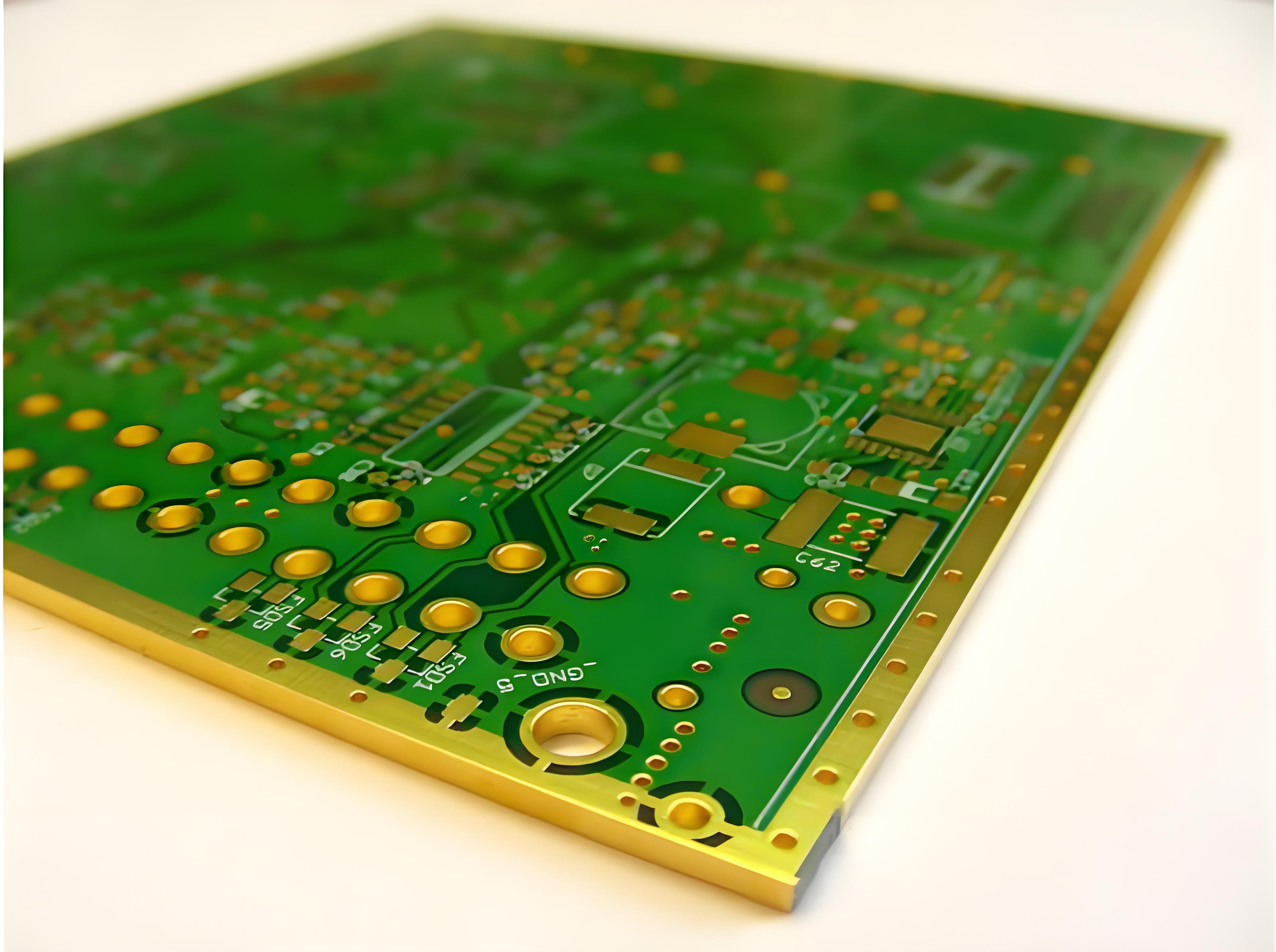
In a PCB, exposed copper refers to areas where the copper layer is intentionally left uncovered by solder mask or surface finish. Normally, copper traces and pads are coated with a protective layer to prevent oxidation and corrosion. However, in certain parts of the board, copper is left exposed for electrical or mechanical reasons.
You’ll typically see exposed copper in places where components need to be soldered or where the board makes direct contact with another surface, such as in connectors or test points. These areas must have direct electrical contact, and that means the copper needs to remain accessible.
Where Is Copper Usually Exposed?
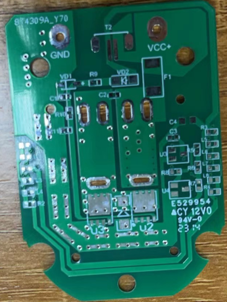
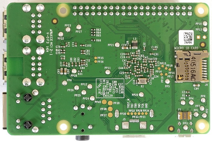
- Component pads: These areas must be exposed for soldering.
- Test points: Used for measuring signals during testing.
- Thermal reliefs: Copper areas used to help dissipate heat.
- Edge connectors: Known as pcb exposed copper edge, these are found on plug-in boards.
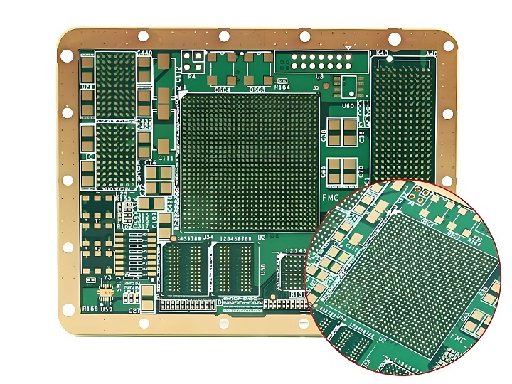
- Copper pours: Large copper areas, sometimes left exposed to improve thermal or grounding performance.
Purpose of Designing Exposed Copper on PCB
Designing with exposed copper is a common and often necessary practice. Below are some of the most common reasons designers choose to expose copper on a PCB.
1. Electrical Contact
Soldering requires exposed copper. All component pads, whether for surface mount or through-hole components, need to be bare so solder can properly adhere and form a good electrical connection.
In addition to pads, test points are exposed copper areas used during assembly and troubleshooting. Probes can be placed on these spots to measure voltages or signals.
2. Thermal Management
Copper is an excellent conductor of heat. In high-power applications, such as LED lighting, motor drivers, or power supplies, leaving copper exposed can help manage heat by allowing it to dissipate more efficiently. Large exposed copper plates can act like heat sinks.
3. Grounding and Shielding
In many designs, especially in radio frequency (RF) or high-speed digital circuits, exposed copper design PCB layouts include areas for grounding or electromagnetic interference (EMI) shielding. A pcb exposed copper edge can also be connected to ground and used as part of the shielding structure to protect signal integrity.
4. Cost Considerations
Leaving copper exposed in non-critical areas can reduce costs. Surface finishes like ENIG or HASL add expense, so in low-cost or temporary boards, some copper may be left bare to save on manufacturing steps.
Types of Exposed Copper PCB Designs
There are several ways exposed copper is used in PCB layouts, each serving a specific function depending on the design goals. Below are the most common types you’ll find, along with their applications and things to watch out for.
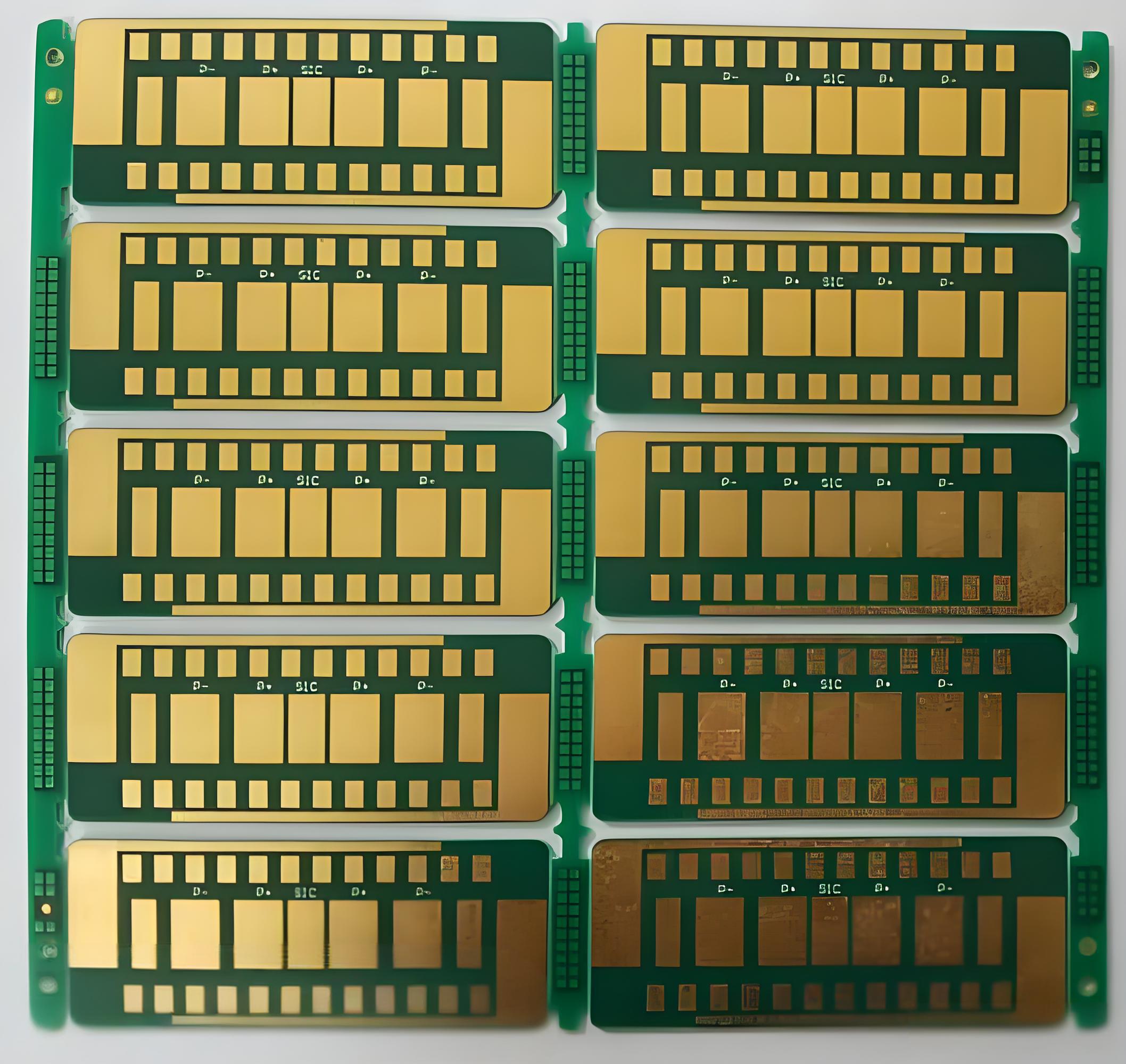
1. Exposed Copper Pads
Exposed copper pads are the most widely used type of exposed copper in any PCB. These are the metal areas where components are soldered onto the board. By design, they must remain uncovered to allow solder to create a solid electrical and mechanical connection between the component leads and the PCB’s copper layers.
In addition to component soldering, some exposed pads are used for mechanical support or to connect heat-generating parts to large copper pours for better heat dissipation. Proper surface finish on these pads—such as HASL or ENIG—helps prevent oxidation and improves solderability.
2. Exposed Copper Traces
In some designs, traces (the thin copper lines connecting different components) are intentionally left exposed. This is less common than exposed pads, but it’s done in specific cases where designers need direct access to the trace for testing or where the trace carries high current and benefits from better heat dissipation.
One common use for exposed copper traces is creating test points. By leaving a section of trace uncovered, engineers can place probes directly on the trace during testing or troubleshooting.
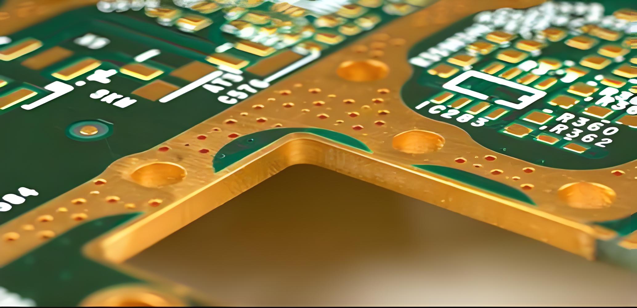
3. PCB Exposed Copper Edge
A pcb exposed copper edge refers to copper that runs right to the edge of the PCB and remains exposed for functional use. This is typically found in boards that need to connect to sockets or other boards via edge connectors. In these cases, the copper along the edge acts as contact points and must remain exposed for reliable electrical connection.
This type of exposed copper is also used for grounding purposes. For example, in RF circuits or high-speed digital designs, the board edge may have exposed copper connected to ground to reduce electromagnetic interference (EMI). Some designs use edge plating, where the copper is plated along the entire edge of the board to create a continuous conductive path.
What Is the Clearance of Copper to Edge of PCB?
When designing PCBs, copper-to-edge clearance is critical. Copper should not be placed too close to the edge unless it is meant to be exposed. If copper unintentionally gets too close to the edge, it can cause manufacturing problems or failures in the field.
Industry Guidelines
Standard practice, according to IPC standards, recommends at least 0.25mm (10 mils) clearance between copper and the board edge. This clearance prevents copper from being damaged or exposed during board cutting.
Edge Copper Design
If you’re designing a pcb exposed copper edge, such as for a connector or grounding point, you can extend copper to the edge, but it must be plated and processed correctly. Special instructions are needed for the manufacturer to plate the edges and prevent delamination.
How to Design a PCB with an Exposed Copper Plate?
Designing exposed copper areas requires planning and proper use of your PCB design software.
Step 1: Define Copper Areas
Use copper pours, pads, or large planes for the areas you want exposed. Ensure they are connected to the correct net, whether ground, power, or signal.
Step 2: Disable Solder Mask
In your PCB layout tool, disable the solder mask over these areas. This is done by creating a solder mask opening in the relevant layer.
Step 3: Edge Exposure
For pcb exposed copper edge designs, extend the copper to the edge of the board. Indicate this clearly in your mechanical drawings. Some manufacturers require a note to plate the edge.
Step 4: Selective Surface Finish
Decide whether the copper will remain bare or have a finish like HASL (Hot Air Solder Leveling) or ENIG (Electroless Nickel Immersion Gold). These finishes prevent oxidation and improve durability.
Risks and Challenges with Exposed Copper PCB
While exposed copper on PCB serves many useful purposes, it comes with challenges.
Oxidation and Corrosion
Copper oxidizes quickly in air, forming a dull brown or green layer. This can reduce conductivity and make soldering difficult. Moist environments accelerate this process.
Short Circuits
Exposed copper is more likely to cause shorts if it touches other metal objects. Extra care is needed in design and assembly to avoid accidental contact.
Handling Risks
Bare copper areas can be scratched or contaminated during handling. Fingerprints, dust, or moisture can affect performance. Protective packaging and careful assembly help reduce these risks.
Exposed Copper Design Guidelines in PCB Layout
Here are some helpful tips for designing exposed copper areas safely:
- Maintain clearance from high-voltage areas unless insulation is provided.
- Use protective coatings like conformal coating if the board will be exposed to harsh environments.
- Clearly indicate exposed copper areas in your Gerber files and fabrication notes.
- For pcb exposed copper edge, work with your manufacturer to ensure proper plating and durability.
- Use thicker copper (e.g., 2 oz) for large exposed areas meant for heat dissipation or high current.
FAQs
1. How to remove copper from PCB board?
Copper can be removed through chemical etching using ferric chloride or similar solutions. It can also be scraped off mechanically or milled with CNC tools.
2. What happens to exposed copper?
Exposed copper oxidizes when exposed to air and moisture. This can affect electrical performance, so protective finishes or coatings are often applied.
3. Can exposed copper PCB be used outdoors?
Not directly. Outdoor use requires additional protection, like conformal coating, to prevent corrosion. Without protection, copper will degrade quickly.
4. How do I prevent oxidation on exposed copper areas?
Apply coatings such as OSP (Organic Solderability Preservative), clear lacquer, or conformal coating. Using surface finishes like ENIG or HASL also helps.
5. What surface finish is best if I want partial copper exposed?
ENIG and HASL can be applied selectively. Masking during the finishing process allows partial copper exposure where needed.
6. Is exposed copper safe for high-voltage applications?
Not unless proper spacing and insulation are used. High voltage requires strict clearance and protection to avoid arcing or shorts.
7. What’s the difference between exposed copper and plated finish?
Exposed copper has no added layer, while plated finishes like ENIG or HASL add protection and improve performance.