

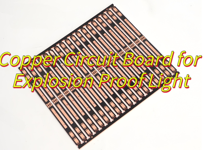
Why choose copper circuit board for explosion proof light? Let’s explore benefits, applications, design guide, thermal management, production processes, cost reduction methods for copper circuit board.
Are you worried about these issues?
- Frequent circuit failures due to high temperatures?
- Repeated failures in explosion-proof certification?
- High maintenance costs?
EBest Circuit (Best Technology) can provide solution:
- Our copper substrate optimizes the heat dissipation structure to reduce chip junction temperature by 30%, extending lamp life.
- Our copper substrate undergoes pre-testing and verification, passing spark tests and EMC testing in a single pass, reducing certification cycles by 50%.
- Our copper base plate extends lamp life by 30% and reduces annual maintenance costs by 45%, achieving long-term cost reduction.
Welcome to contact us if you have any inquiry for copper circuit board: sales@bestpcbs.com.
Why Choose Copper Circuit Board for Explosion Proof Light?
- Instant Heat Dissipation: Copper’s 401 W/m·K thermal conductivity rapidly pulls heat from LEDs, preventing dangerous temperature spikes in enclosed, flammable spaces.
- Chemical & Salt Resistance: Natural copper patina and protective coatings (e.g., ENIG) block corrosive gases, oils, and saltwater—ideal for offshore platforms or chemical plants.
- Vibration-Proof Design: Thicker copper traces (2oz–4oz) and rigid substrates resist cracking from constant machinery vibrations, unlike fragile FR4 boards.
- Extreme Temperature Stability: Operates reliably from -40°C (arctic drilling sites) to 150°C (desert refineries) without warping or delamination.
- High Current Efficiency: Superior electrical conductivity minimizes energy loss, crucial for power-hungry explosion-proof fixtures in remote locations.
- Precision Circuitry: Fine-pitch traces (≤0.1mm) support complex LED driver designs while maintaining structural integrity under thermal stress.
- Long-Term Cost Savings: Fewer replacements due to corrosion or heat failure reduce maintenance costs over the product’s 10+ year lifespan.
Applications of Explosion Proof Light Copper Circuit Board
- Oil & Gas Rigs: Keeps LEDs cool in offshore platforms, resisting saltwater and flammable hydrocarbons.
- Chemical Plants: Stabilizes LEDs in explosive atmospheres, withstanding aggressive solvents and acids.
- Underground Mines: Endures machinery vibrations in methane-rich tunnels with thick copper traces.
- Pharmaceutical Labs: Provides sterile, corrosion-resistant lighting for labs handling volatile materials.
- Marine Vessels: Powers reliable LED navigation lights in humid, fuel-vapor-prone environments.
- Grain Storage: Prevents dust explosions by dissipating LED heat below combustible particulate thresholds.
Explosion Proof Light Copper Circuit Board Design Guide
Below are explosion proof light copper circuit board design guide:
1. Material Selection
- Prioritize copper baseboards with 2oz (70μm) or thicker copper, with critical current paths increased to 3oz (105μm) to reduce impedance and heating risks.
- Recommended substrates: modified FR-4 or polyimide (PI), offering high-temperature resistance and mechanical durability to prevent delamination during thermal cycling.
2. Safety Spacing Design
- Electrical Clearance: ≥2.5mm for high-voltage areas (≤250V) or ≥5mm (250V-500V).
- Creepage Distance: Increase by 20% in humid conditions to prevent surface discharge.
3. Heat Dissipation & Layout
- Mount LED driver chips directly on the copper baseboard using thermal silicone (thermal resistance <1.5℃/W).
- Follow IPC-2152 standards for current-carrying capacity (e.g., 4mm trace width for 50A at 3oz copper thickness).
4. Explosion-Proof Structure Adaptation
- Maintain ≥3mm buffer space between PCB edges and explosion-proof housing walls to avoid friction sparks.
- Apply conformal coating (moisture/salt spray/mildew resistant) to all solder joints; use ceramic-filled adhesive in corrosive environments.
5. EMC & Noise Immunity
- Keep high-frequency signal traces ≥2mm away from power lines; use shielding or slot isolation if needed.
- Ensure ≥6.4mm spacing between primary and secondary sides of optocouplers/Y capacitors, or implement slot isolation.
6. Manufacturing Requirements
- Roughen the copper-to-substrate interface (Ra 1-3μm) to achieve peel strength >1.2N/mm.
- Avoid sharp corners; use 45° or rounded turns to minimize corona discharge risks.
7. Testing & Validation
- Pass 1,000 cycles of -40℃~125℃ thermal shock testing to verify copper-substrate adhesion.
- Conduct spark testing (per IECEx certification) to confirm no potential ignition sources.
Thermal Management Explosion Proof Light Copper Circuit Board
High-Thermal-Conductivity Copper Substrate Selection
- Use 35μm~280μm thick copper foil (thermal conductivity ≥385W/m·K) for rapid heat dissipation.
- Prioritize metal core PCBs (MCPCBs) over traditional FR4 to enhance overall thermal performance.
Low-Thermal-Resistance Layout Design
- Place high-power components (e.g., LEDs, MOSFETs) near heat dissipation channels or metal enclosures.
- Avoid heat source clustering; distribute devices evenly with adequate airflow gaps.
Thermal Groove & Structural Design
- Mill elliptical/rectangular explosion-proof grooves (≥7mm from board edges) to release internal vapor pressure under high temperatures.
- Integrate groove processing with CNC machining for precision, preventing delamination.
Thermal Vias & Copper Pour Optimization
- Integrate 1.5mm-diameter heat pipes filled with phase change materials (PCMs) in high-power zones, limiting local temperature rise to ≤15°C.
- Use alternating 0.2mm/0.4mm via arrays with ≥30μm copper plating on hole walls to reduce interlayer thermal resistance.
Surface Treatment & Thermal Interface Materials
- Apply immersion gold, tin plating, or OSP to prevent oxidation and improve solderability.
- Fill gaps between heat sources and heat sinks with thermal grease or PCMs to minimize contact resistance.
Active Cooling Integration
- Attach aluminum heat sinks with fins to enclosures, paired with heat pipes or fans for accelerated heat diffusion.
- For extreme scenarios (e.g., 5G base stations), adopt liquid cooling or hybrid heat pipe + fan systems.
How to Balance Cost and Quality for Explosion Proof Light Copper Circuit Board?Thermal Resistance Modeling & Validation
- Optimize heat dissipation paths using improved parallel thermal resistance models.
- Verify performance via dielectric strength tests and AOI inspections to meet explosion-proof standards.
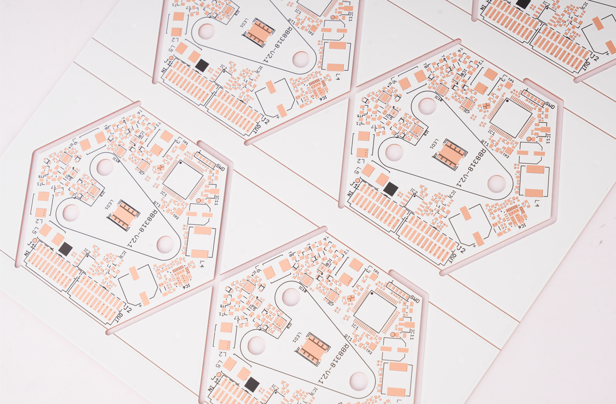
Explosion Proof Light Copper Circuit Board Manufacturing Processes
1. Cutting: Cut copper substrate raw materials into required production sizes, ensuring flat and defect-free plates.
2. Drilling: Use mechanical or laser drilling machines to create component holes, through-holes, and explosion-proof groove Reserved holes.
3. Chemical Copper Plating: Deposit a thin copper layer on hole walls and surfaces to form conductive layers.
4. Circuit Imaging: Apply photosensitive dry film to the copper substrate. Expose and develop to retain desired circuit patterns.
5. Etching: Chemically remove unprotected copper foil to form precise circuits.
6. Film Stripping: Remove residual dry film to expose complete copper circuits.
7. Surface Treatment: Choose immersion gold, tin plating, or OSP (Organic Solderability Preservative) to prevent oxidation.
8. Solder Mask Printing: Apply green solder mask ink to protect non-soldering areas.
9. Silkscreen Printing: Print component identifiers and symbols for assembly/maintenance.
10. CNC Machining: Cut circuit boards to final shapes using CNC for dimensional accuracy.
11. Explosion-proof Groove Processing: Mill elliptical/rectangular grooves ≥7mm from board edges.
12. HASL (Hot Air Solder Leveling): Coat and flatten solder for uniform welding layers.
13. Dielectric Strength Test: Verify insulation performance and electrical safety per explosion-proof standards.
14. Final Testing: Electrical Test or AOI Inspection.
15. Packaging: Anti-static packaging for safe transportation.
How to Balance Cost and Quality for Explosion Proof Light Copper Circuit Board?
Material Optimization
- Base Substrate: Use C110 copper (1.0–1.5mm thickness) instead of premium alloys for cost efficiency.
- Surface Finish: Opt for HASL-LF (lead-free) instead of ENIG if corrosion resistance is adequate.
Design Simplification
- Trace Layout: Reduce non-critical copper layers (e.g., 2-layer instead of 4-layer) while maintaining thermal paths.
- Via Count: Minimize thermal vias in low-heat zones using thermal simulation tools.
Process Efficiency
- Panel Utilization: Nest multiple PCBs per panel to reduce material waste.
- Batch Production: Consolidate orders for ENIG or electroplating to lower per-unit costs.
Supplier Collaboration
- Local Sourcing: Partner with regional copper suppliers for competitive pricing.
- Long-Term Contracts: Negotiate bulk discounts for C110 copper sheets and surface finish chemicals.
Compliance Targeting
- Certification Scope: Achieve ATEX/IECEx compliance for gas (Zone 1) only if dust (Zone 21) isn’t required.
- Testing Reduction: Use modular design to test sub-assemblies instead of full fixtures.
Defect Reduction
- Process Controls: Implement SPC (Statistical Process Control) for etching and plating lines.
- Inspection Automation: Use AOI (Automated Optical Inspection) for solder mask and trace defects.
Lifecycle Management
- Prototyping: Build cost-effective prototypes with FR4 substitutes for initial testing.
- Feedback Loops: Use field data to refine designs and avoid over-engineering.
Why Choose EBest Circuit (Best Technology) as Copper Circuit Board Supplier?
Reasons why choose us as copper circuit board supplier:
- 19 Years of Technical Mastery: Leverage proven expertise in explosion proof light copper circuit board and patented explosion-proof technologies.
- Global Compliance Certifications: Streamline market entry with pre-certified ISO/RoHS/REACH/UL products, mitigating legal and regulatory risks.
- 24-Hour Rapid Prototyping: Accelerate innovation cycles with functional prototypes delivered overnight, enabling immediate testing, iteration, and design validation.
- 7-Day Mass Production Scalability: Reduce time-to-market by 70%+ through agile production scaling, meeting urgent demand without compromising precision (e.g., 50,000㎡ annual capacity).
- Thermal Performance Optimization: Eliminate overheating risks in high-power applications (e.g., LEDs, 5G modules) via heat pipes, PCMs, and low-thermal-resistance layouts.
- Free DFM Analysis: Prevent costly delays by identifying design flaws early, ensuring seamless transition from concept to manufacturing.
- End-to-End Turnkey Service: From PCB layout (supporting Altium/PADS) to thermal simulation (ANSYS Icepak) and assembly. Simplify vendor management for complex lighting systems.
- Cost-Effective Premium Solutions: Direct factory pricing without middlemen. Balance high-performance materials (e.g., 3W/m·K aluminum) with budget-friendly options for mass production.
Welcome to contact us if you have any inquiry for copper circuit board: sales@bestpcbs.com.