

An EV thick copper substrate is really important in the AVs, such as the application of battery management systems, on-board chargers, DC-DC converters, motor controllers, thermal management systems, and others. In this blog, we will discuss valuable information, including the structure, features, thickness standards, selection guide, and key applications of EV thick copper substrates, to ensure better performance in electric vehicles.
Have you run into these problems when working on the EV PCB projects?
- The drilling process problems, such as the inner layer cracks, rough hole walls, and the damaged drilling bit problem?
- The thermal management challenges, such as the difference in thermal expansion coefficient, may cause solder joint fatigue and affect the equipment’s lifespan.
- The design and the manufacturing complex?
- The shortage of reliability evaluation?
EBest Circuit (Best Technology) provides innovative solutions for tackling the above issues.
- Optimize the drilling process and material selection: use the special drilling parameter and optimize the drilling bit to reduce the problem of inner layer cracks and the rough hold walls problem. Finally, improve the manufacturing efficiency and the product quality.
- Optimize the thermal management and the material selection: employ the high thermal material and the thermal management design to improve the thermal expansion efficiency.
- Control process and the quality: Make use of laser thickness measurement, dynamic compensation systems, and the full process parameter traceability to ensure the precision of the copper thickness control and the product quality.
- Make the reliability evaluation and the accelerated inspection.
EV thick copper substrate plays a vital role in the electric vehicle sector. If you have any more technical questions or any inquiries, just feel free to contact EBest Circuit (Best Technology) via sales@bestpcbs.com. EBest Circuit (Best Technology) has specialized in thick copper PCB prototype, manufacturing, assembly, and box build service for over 19 years. Looking forward to hearing from you!
What is EV Thick Copper Substrate?
An EV thick copper substrate is a printed circuit base material built with extra layers of copper. Generally, the copper thickness of the common PCB ranges from 1 OZ to 3 OZ, however, in the EV, the copper thickness can be up to 6 OZ to even 20 OZ. This thicker copper layer can manage the high current without being damaged, to reduce the energy loss, and improve the safety margins. In essence, the EV thick copper substrate is the core of the EV power management.
What are Features of Copper Substrate PCB?
A copper substrate PCB is recognized for its outstanding thermal conductivity. The heat can be conducted quickly, and protect the sensitive chips. It also has remarkable current-carrying ability, which is a core need for EV power modules. Besides, its mechanical strength is higher than the common FR4 as well. The designers commonly select this copper substrate PCB when facing the high reliability requirements. The EV system’s lifespan will be extended by using this PCB.
What is the Composition of EV Thick Copper Substrate?
EV thick copper substrate is made of three layers, including heavy copper foil, insulation dielectric, and the substrate, such as aluminum or FR4. The copper layer decides the current loading capability. And the insulation dielectric is responsible for the insulation and the thermal dissipation. The substrate provides the stability, however. To some designs, there will increase in the protected coating to improve the corrosion resistant. It is good to know that each layer is vital to the stable performance in the hard EV environment.
What are the Types of EV Thick Copper Substrate?
EV thick copper substrates come in several types:
As per structure:
- Single-sided thick copper PCB – for simple, high-current circuits.
- Double-sided thick copper PCB – when routing density increases.
- Multilayer thick copper PCB – designed for advanced EV powertrain and battery management systems.
As per the material compound:
- The hybrid copper substrate – Combining copper and aluminum to boost the heat dissipation performance.
- Ceramic substrate (DBC/AMB) – It is bonded by combining DBC and Al₂O₃/AlN ceramic, suitable for high-temperature and high-power applications.
Different type meets different project needs. Choose the suitable one as per the design complexity, electrical press grade, and the durability requirements.
How Much Thick Copper PCB in an EV?
In an electric vehicle, thick copper PCBs are used in several areas. For example, the battery module, automobile charger, and DC-DC converter. The amount varies by vehicle model. High-performance EV in the power control unit and motor drive modules will use the thicker copper PCBs. The lighting system, when dealing with the current surges, will get its benefits as well. Generally, multiple thick copper PCBs are present throughout the EV system.
How Thick Should EV Thick Copper Substrate Be?
The required EV thick copper substrate thickness depends on the specification designed. The common range is from 4 OZ to 12 OZ. High power applications, such as main inverters, may require 15 OZ or even higher. The engineers will decide according to the current needs, heat output, and the space limit. A reasonable copper thickness can get a balance between efficiency and cost. Since the thinner will get the risk of over heating, but the thicker will increase the costs.
PCB Copper Thickness Chart
The following is the simplified PCB copper thickness chart:
| Copper Weight (OZ) | Thickness (µm) | Common Application |
| 1 OZ | 35 µm | Low-current signal circuits |
| 3 OZ | 105 µm | Medium power modules |
| 6 OZ | 210 µm | Battery controllers, power relays |
| 10 OZ | 350 µm | EV inverters, motor drivers |
| 15+ OZ | 525 µm+ | Heavy-duty EV systems |
This chart helps engineers select the suitable copper thickness according to the current and the heat dissipation needs. It provides a clear reference during the stage of selecting substrate types.
How to Select EV Thick Copper Substrate for the Project?
When selecting an EV thick copper substrate, several factors come into play:
- Required copper thickness based on current load.
- Thermal conductivity to manage hot spots.
- Mechanical strength for vibration resistance.
- Cost efficiency and guarantee the safety in the meantime.
It needs to consider the space limit inside the EV part when designing. EBest Circuit (Best Technology) helps customers balance all these concerns. Customers often meet the pain point, such as over-heating boards and the traceability difficulty. Our MES system addresses this by tracking every stage of production. We also control the copper-plated uniformity strictly, so as to reduce the failure risks. Then customers don’t need to bear the extra cost for the rework.
What are the Specific Applications for EV Thick Copper Substrate?
Thick copper PCB is widely used in EVs, mainly including:
- BMS: Solving the high current charging and discharging.
- Main Inverter: Provide controlled power to the driving motor.
- Automobile Charger: Ensure safety during charging.
- Heat Management System: Keep the battery within the safe temperature ranges.
These applications have extremely high requirements for the substrate strength, durability, and precision. Using EV thick copper substrate, the EV manufacturers can get higher efficiency, more better safety, and more longer lifespan of the components.
Case about EV Thick Copper Substrate
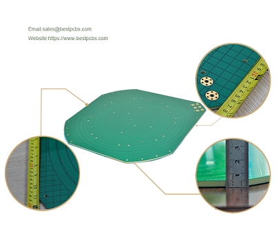
EBest Circuit (Best Technology) has valuable experience in the EV Thick Copper Substrate PCB cases. Here are some parameters of the thick copper PCB that our customers used in some of their projects. You can take it as a reference. If any help is needed, please feel free to let us know, and we will provide the specific boards and solutions according to your project requirements.
Extra Heavy Copper (14L 5.588mm+/-10% ≥5 OZ) FR4 PCB Parameters
- Layers: 14 layers heavy copper PCB
- Inside and outside copper are different, over 5OZ
- Board Thickness: 5.588mm+/-10%
- Surface Treatment: ENIG
- Solder Mask: Green oi
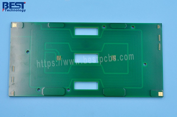
14 Layers heavy copper PCB Parameters
- Layers: 14 Layers heavy copper PCB
- Materials: Tg170
- board thickness: 6.9mm+/-10%,
- 4oz copper at each layer
- Surface Treatment: Immersion gold (Au 2u”)
- Solder Mask: Green solder mask, white silk screen.
- Application: High power supply
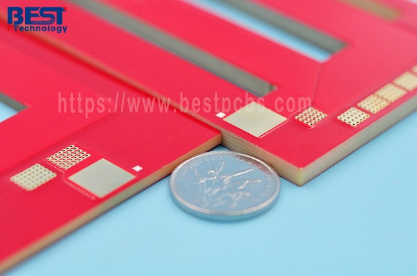
8L Heavy Copper PCB Parameters
- Materials: Tg170
- Board Thickness: 2.55mm+/-10%,
- 4oz copper at each layer
- Surface Treatment: Immersion Gold (Au 2u”)
- Solder Mask: Red solder mask, white silk screen.
- Application: High Power Supply
To sum up, the EV thick copper substrate is the core of EV safety, high efficiency, and powerful operation. It is not only a circuit material. EV gains a competitive edge in durability and performance through selecting the suitable copper thickness and the substrate designs. EBest Circuit (Best Technology) has our own PCB factory, fully compliant with ISO 9001, ISO 13485, IATF 16949, AS9100D, UL, REACH, and RoHS standards. If you need a reliable manufacturer for a viable solution, just feel free to contact us via sales@bestpcbs.com.