

What is embedded copper coin PCB? Let’s explore its structure, benefits, applications, connector methods, design guide, production processes together.
Are you troubled with these problems?
- Is your product throttled by poor heat dissipation?
- Are traditional cooling solutions squeezing your design space?
- Is your PCB frequently experiencing thermal failures under complex operating conditions?
EBest Circuit (Best Technology) can offer services and solutions:
- Customized thermal design: ANSYS simulation and field verification.
- Flexible manufacturing services: 0.2-2.0mm copper coin options.
- Full-process quality control: 16 critical process checks for reliability.
Welcome to contact us if you have any inquiry for embedded copper coin PCB: sales@bestpcbs.com.
What is Embedded Copper Coin PCB?
Embedded Copper Coin PCB (Embedded Copper Coin) is an innovative technology that improves heat dissipation by embedding copper sheets (called “copper coins”) within printed circuit boards (PCBs). These copper coins, typically in a circular or rectangular stepped design, efficiently absorb and dissipate heat generated by electronic components, making them particularly suitable for high-power devices or miniaturized products (such as 5G communications equipment and space electronics).
This technology leverages copper’s high thermal conductivity to mount heat-generating components directly on the copper coins, significantly overcoming the limitations of traditional PCB heat dissipation vias or metal substrates, achieving more compact and efficient heat dissipation.
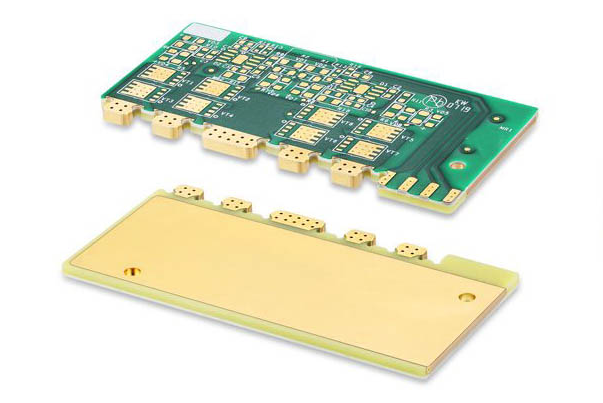
Structure of Embedded Copper Coin PCB
1. Copper Coin Body
- Material: ≥99.9% pure copper, 0.5–3mm thick, 5–20mm diameter, nickel-plated.
- Design: Stepped profile expands heat contact; fits round/rectangular chips.
2. Embedding Process
- Process: Laser/mechanical insertion into PCB layers, FR-4 bonded, resin-filled for flatness.
- Tolerance: Adhesive residue ≤0.1mm to prevent via cracks.
3. Conductive Interconnects
- Vias: Metallized, copper-plated ≥25µm for low impedance.
- Clearance: ≥0.2mm between layers (3kV AC safe).
4. Insulation & Protection
- Solder Mask: ≥15µm edge coverage.
- Vias: Resin-filled to reduce thermal stress.
5. Thermal Management
- Path: Thermal adhesive/aluminum substrate beneath coin for vertical cooling.
- Stacked Design: Simulation-optimized heat flow.
Advantages of Copper Coin-Embedded PCB
- Highly Efficient Heat Dissipation: Copper exhibits excellent thermal conductivity and is embedded directly beneath heat-generating components to quickly dissipate heat and prevent overheating damage (such as power ICs or automotive-grade chips).
- Saves PCB Space: No additional heat sink or complex air cooling systems are required, making it suitable for compact designs (such as drones and portable devices).
- Improves Long-Term Reliability: Copper and PCB materials have similar coefficients of thermal expansion, reducing the risk of solder joint cracking and extending product life.
- Lowers Overall Cost: The process is simpler than embedded copper coins, reducing production steps and material waste.
- Supports Custom Design: Round and rectangular copper coins can flexibly adapt to different component shapes (such as special-shaped chips) to optimize heat conduction paths.
Applications of Embedded Copper Coin PCB
- High-Power LED Lighting Cooling
- RF/Microwave Power Amplifiers
- New Energy Vehicle Power Systems
- Industrial Power Equipment
- Aerospace Electronics Systems
- Server Power Modules
- Power Electronics Converters
- High-density packaged device cooling
- Automated test equipment (ATE)
- Audio power amplifiers
How is the Copper Coin Connected to the PCB?
Metallized Via Direct Connection
- Copper coins connect to PCB inner layers via laser-drilled microvias (aperture ≥0.3mm), with copper plating thickness ≥25µm on via walls, ensuring low-impedance conduction (<10mΩ).
- Suitable for high-current applications (e.g., EV traction systems carrying ≥200A).
Stepped Laminated Structure
- Adopts OKI’s stepped copper coin design, where copper coins are laminated with PCBs using resin-filled gaps. Contact diameter 7mm, heat dissipation expanded to 10mm.
- Requires controlled lamination temperature (170–200℃) and pressure (200–400psi) to avoid resin voids and elevated thermal resistance.
Conductive Adhesive Bonding
- Uses thermal conductive adhesive (e.g., 3M 8810, thermal conductivity ≥1.5W/mK) to fix copper coins in non-conductive areas.
- Ideal for high-frequency signal modules (e.g., mmWave radar) to prevent electromagnetic interference from metal vias.
How to Design A Embedded Copper Coin PCB?
Below are embedded copper coin PCB design guide:
1. Material & Copper Coin Parameter Design
- Material selection: Select ≥99.9% purity electrolytic copper (thermal conductivity: 401W/(m·K)), with thickness matched to chip power (e.g., 1.5mm for 10W chips, 2.5mm for 20W chips).
- Surface treatment: Nickel-plated (≥5µm); gold plating (≥1µm) for extreme environments.
- Shape optimization: Stepped design expands contact area by 30–50%; rectangular coins for linear-package devices.
2. Embedding Position Planning
- Single-layer boards: Align copper coin center with high-power component (e.g., CPU/GPU) heat core (error ≤0.2mm).
- Multi-layer boards: Vertically stagger coins (e.g., Layer 2 coins offset 5mm from Layer 1).
- Safety clearance: Maintain ≥0.5mm gap between coin edges and high-speed signal lines; ≥2mm from PCB edges.
3. 3D Thermal Interface Design
Vertical Cooling:
- Apply thermal adhesive (e.g., Arctik 8800, 3.0W/(m·K)) to fill micro-gaps between chip and coin.
- Embed aluminum substrate (1.0mm thickness) beneath coins; connect to backside heatsinks via thermal vias.
Horizontal Cooling:
- Array small coins (3mm diameter, 5mm pitch) under uniformly heated devices (e.g., FPGAs).
- Deploy thermal via arrays (0.3mm diameter, 0.8mm pitch) around coins; fill with conductive epoxy (e.g., Ausbond 9105, 1.5W/(m·K)).
4. Thermal Via Optimization
- Via parameters: Diameter ≥0.3mm, copper plating ≥25µm, depth ≤2/3 of PCB thickness.
- Process enhancement: Electroless Nickel Immersion Gold (ENIG) finish for via walls; array vias in ring or matrix patterns (pitch ≤1mm).
5. Manufacturing Process Control
Embedding methods:
- Small coins (≤5mm): Laser drilling (±0.05mm accuracy), vacuum-adhesive fixation.
- Large coins (≥10mm): Mechanical pressing (50–80psi), alignment pins for hole matching.
Resin filling: Use low-CTE (≤40ppm/℃) epoxy to fill gaps; cure via baking (150℃, 2 hours).
6. Thermal Simulation & Validation
- Simulation phase: Model steady/transient thermal distribution using Ansys Icepak (input material parameters, via layout, and chip power data).
Physical testing:
- Thermal imaging: Ensure junction-to-coin ΔT ≤5℃ (e.g., coin ≤115℃ at chip 120℃).
- Temperature cycling (-40℃~125℃, 1,000 cycles): Inspect for cracks/delamination at coin-PCB junctions.
7. Standards Compliance Testing
- Compliance: CPCA 6042 (embedded copper PCBs), IPC-6012C (rigid PCBs).
- Dielectric testing: Apply 3kV AC between adjacent coins/ground; no breakdown for 60 seconds.
What is the Process of Embedded Copper Coin PCB?
1. Substrate Preprocessing & Copper Coin Fabrication
- Substrate Cutting: FR-4 substrate cut to working dimensions (tolerance ±0.1mm), with simultaneous milling of copper coin positioning slots (depth = coin thickness +0.05mm).
- Copper Coin Machining: CNC-shaped electrolytic copper (C11000), surface nickel-plated (2–5μm) + chemical roughening (Ra 0.8–1.2μm).
2. Inner Layer Production & Coin Embedding
- Inner Layer Imaging: After circuit etching, black oxidation treatment applied to copper coin zones (surface area increased ≥30%).
- Coin Assembly: Vacuum nozzle with visual positioning system (accuracy ±25μm) presses coins into slots; edges coated with conductive epoxy (thermal conductivity ≥5W/mK).
- Pre-Lamination Inspection: X-ray detection of coin positional deviation (standard ≤0.1mm).
3. Multi-Layer Lamination Control
Stack-Up Structure: 2 high-TG prepreg sheets (e.g., IT-180A) placed above/below copper coin layer; copper foil pre-laminated with thermal adhesive film.
Vacuum Hot Pressing Parameters:
- Stage 1: 120℃ / 3MPa / vacuum ≤10Pa
- Stage 2: 180℃ / 8MPa / dwell 60min
- Stage 3: Cooling to <50℃ before pressure release
Post-Pressing Treatment: Laser trimming of resin overflow; plasma cleaning of coin zones.
4. Drilling & Metallization
Step Drilling:
- φ0.3mm pilot holes (through coin center)
- Enlarged to φ0.5mm (aspect ratio ≤12:1)
- Back-drilling residue ≤0.15mm
High-Thermal Via Metallization:
- Pulse copper plating (average thickness ≥30μm)
- Via filling with silver paste (thermal conductivity >200W/mK) or nano-aluminum resin.
5. Outer Layer Circuitry & Thermal Enhancement
- Laser LDI Imaging: Circuit width compensation +0.1mm at coin connection zones (to offset lamination deformation).
- Selective Thick Copper Plating: 3oz (105μm) plating around coin zones; 1oz (35μm) retention at non-thermal zones.
- Thermal Via Arrays: φ0.25mm vias (pitch 1.0mm) within 1mm of coin edges, filled with thermal paste.
6. Surface Finish & Testing
Coin-Specific Surface Treatment:
- Electroless nickel-palladium-gold (ENIG: Ni 5μm/Pd 0.2μm/Au 0.05μm) .
- Or OSP + localized silver plating for oxidation resistance.
Thermal Validation:
- Infrared thermography (ΔT ≤12℃ under 10W input)
- Thermal cycling (-55℃~125℃, 1,000 cycles; impedance change ≤3%)
7. Final Inspection & Packaging
- Coin-Specific Testing: Ultrasonic scanning (detect delamination); Shear strength test (≥50N/mm²)
- Packaging: Antistatic vacuum packaging (internal humidity ≤10%RH); silicone pads added to coin zones.
Why Choose EBest Circuit (Best Technology) as Embedded Copper Coin PCB Supplier?
Reasons why choose us as embedded copper coin PCB supplier:
- Certification Compliance: ISO 9001, IATF 16949, ISO 13485 and RoHS, UL certified, and ensures global market compliance and reliability.
- Superior Material Quality: Use ≥99.9% electrolytic copper (C11000) with nickel/gold plating. Ensures superior thermal conductivity (≥401W/m·K) and long-term reliability.
- Reliable Quality Control: Strict process control with AOI/SPI/X-Ray inspection ensures 99.5% assembly yield and minimal defects.
- 24 Hours Rapid Prototyping: Accelerates product launches and time-to-market.
- Free DFM Optimization: Reduces design errors by 40% and avoids costly rework.
- One-Stop Solution: Simplifies vendor management, cutting admin work by 60%.
- Advanced Thermal Solution: Guarantees stability for high-power applications (e.g., automotive/5G).
- 24/7 Technical Support: Minimizes downtime and ensures smooth mass production.
Welcome to contact us if you have any request for embedded copper coin PCB: sales@bestpcbs.com.