

Seeking for embedded boards solutions for your project? This guide explores their definition, components, types, and practical solutions for prototyping, thermal management, and cost optimization, helping you navigate efficient embedded development.
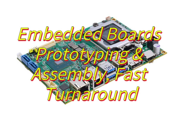
EBest Circuit (Best Technology) specializes in high-speed embedded board prototyping and assembly with guaranteed 24-hour turnaround time, backed by 18 years of industry experience serving 500+ clients annually. Our manufacturing capabilities cover advanced HDI (up to 20 layers), impedance control (±5% tolerance), and thermal management solutions, all produced in ISO 9001-certified facilities with <0.3% defect rates. Transparent pricing structure delivers 15-25% cost savings compared to industry averages, as verified by third-party audits. Testimonials from automotive and medical device clients confirm 30% faster time-to-market using our services. Contact our engineering team today for a no-obligation quote and experience prototype-to-production excellence: sales@bestpcbs.com.
What Is An Embedded Board?
An embedded board is a dedicated computing platform designed to perform specific functions within a larger system. Unlike general-purpose computers, it integrates a processing unit (like a microcontroller or microprocessor), memory, input/output interfaces, and power regulation into a single compact circuit board. These boards operate autonomously with specialized firmware, enabling precise control in applications ranging from medical devices to industrial automation.
This inherent specialization demands rigorous prototyping and precise assembly. Rapid turnaround becomes valuable during development, allowing engineers to test functionality, optimize thermal performance, and validate real-world reliability before full-scale production. Efficient prototyping ensures the final embedded board delivers consistent operation under its intended environmental constraints.
What Are Components of Embedded Boards?
Components of embedded boards:
Microcontroller/Microprocessor
- The “brain” of the embedded board, this chip executes code and manages tasks. Common options include ARM Cortex-M series for low-power devices or ESP32 for Wi-Fi/Bluetooth-enabled boards.
Memory (RAM and Flash)
- RAM: Temporary storage for running programs (e.g., 512MB DDR3 for real-time data processing).
- Flash: Permanent storage for firmware (e.g., 16MB NOR flash for code storage).
Power Management Circuitry
- Includes voltage regulators (to convert 5V/12V inputs to 3.3V logic) and power-on-reset chips to stabilize operation during voltage fluctuations.
Input/Output (I/O) Interfaces
- GPIO Pins: For connecting buttons, LEDs, or sensors.
- Serial Ports: UART for debugging, SPI/I2C for peripherals like displays or EEPROM.
Communication Modules
- Wired: Ethernet PHY, CAN bus for industrial machines.
- Wireless: Wi-Fi 5/6, Bluetooth 5.0, or LoRa for IoT connectivity.
Sensors and Actuators
- Sensors: Temperature (e.g., LM35), motion (MPU6050), or light (BH1750) interfaces.
- Actuators: Motor drivers (L298N) or relay controls for automation.
Clocks and Timers
Real-time clocks (RTC) with battery backups for timestamping, and precision timers for PWM signal generation (e.g., 1kHz motor control).
Protection Components
- ESD Diodes: Guard against static discharge (e.g., 8kV rating).
- Fuses: Resettable PTC fuses for overcurrent protection.
What Are Types of Embedded PCB Boards?
Types of embedded boards:
- Microcontroller Boards: These boards incorporate a microcontroller unit (MCU) with integrated memory and peripherals, making them suitable for basic input/output operations and real-time control in embedded settings, such as home automation or sensor monitoring.
- Single-Board Computers (SBCs): Compact boards that function as complete computing systems, featuring processors, memory, and interfaces, often employed for more demanding tasks in embedded projects like multimedia processing or networking.
- System-on-Module (SoM) Boards: Modular designs that package core computing elements onto a small board, intended for easy integration into larger custom systems, commonly used in scalable embedded solutions for wearables or robotics.
- Development Boards: Purpose-built for prototyping and testing, these boards include accessible pins, sensors, and debugging tools to facilitate experimentation and learning in embedded design environments.
- Evaluation Boards: Designed to assess the capabilities of specific components or chips, these boards help developers evaluate performance and compatibility before finalizing embedded system implementations.
- FPGA Boards: Utilizing Field-Programmable Gate Arrays, these boards allow for customizable hardware logic, enabling adaptable processing for specialized embedded applications like signal routing or real-time control.
- DSP Boards: Focused on digital signal processing capabilities, these boards excel in handling audio, video, or other signal-intensive tasks within embedded systems, such as in communication or medical devices.
Why Choose Embedded Boards Prototyping?
Here are reasons why choose embedded board prototyping:
- Early Functionality Testing – Prototyping allows verification of core features before full production, ensuring the embedded board performs as intended.
- Design Validation – Helps identify and fix hardware and software issues early, reducing costly revisions later.
- Performance Optimization – Enables real-world testing of power consumption, signal integrity, and thermal behavior for refinement.
- Cost Efficiency – Catching flaws early prevents expensive manufacturing errors and reduces overall development expenses.
- Faster Time-to-Market – Accelerates development by allowing quick iterations and validation before mass production.
- Customization Flexibility – Facilitates adjustments for specific needs, such as adding or removing peripherals based on test results.
- Integration Testing – Verifies compatibility with other system components, ensuring smooth operation in the final product.
- Risk Reduction – Minimizes unexpected failures by validating real-world performance under different conditions.
- Iterative Development – Supports gradual improvements based on feedback, leading to a more reliable final embedded board.
How to Optimize Embedded Single Board Computer Prototyping Design to Reduce Costs?
Below are measures to optimize embedded single board computer prototyping design for cost reduction:
Leverage Highly Integrated System-on-Chip (SoC) Solutions
- Select SoCs with built-in peripherals (e.g., Wi-Fi, Bluetooth, GPU) to minimize external components. This reduces board complexity, lowers bill-of-materials (BOM) costs, and simplifies assembly.
- Prioritize SoCs with long-term availability to avoid redesign costs due to component obsolescence.
Adopt Open-Source Hardware and Software Frameworks
- Utilize reference designs from open-source communities (e.g., Raspberry Pi Compute Module, BeagleBone) to accelerate development and reduce engineering hours.
- Use free or low-cost development tools (e.g., Arduino IDE, PlatformIO) and open-source libraries (e.g., FreeRTOS, Linux kernels) to eliminate licensing fees.
Optimize Power Management Design
- Incorporate low-power modes (e.g., sleep, hibernate) and dynamic voltage scaling to extend battery life or reduce energy consumption in always-on applications.
- Use efficient power regulators (e.g., switching regulators instead of linear ones) and optimize PCB layout to minimize power loss.
Standardize Connectivity and Interfaces
- Use universal connectors (e.g., USB-C, HDMI) and industry-standard protocols (e.g., I2C, SPI) to avoid custom cables or adapters, reducing procurement and inventory costs.
- Design for compatibility with existing peripherals (e.g., sensors, displays) to leverage economies of scale and reduce integration risks.
Implement Design-for-Manufacturability (DFM) Principles
- Simplify PCB layout by reducing layer counts and via densities. Use automated design rule checks (DRC) to identify cost drivers (e.g., tight tolerances, non-standard materials).
- Collaborate with contract manufacturers early to optimize component placement and assembly processes, avoiding costly rework.
Prioritize Component Reuse and Scalability
- Develop modular architectures where core functionalities (e.g., processing, memory) are separated from application-specific modules (e.g., I/O boards). This allows reuse across projects and delays customization to later stages.
- Use socketed components (e.g., memory modules) instead of soldered parts to enable easy upgrades and repairs, extending product lifespan and reducing waste.
How to Accelerate Prototyping Cycles for Custom Embedded Development Boards?
Practical measures to accelerate prototyping cycles for custom embedded development boards:
Adopt Modular Hardware Architecture
- Break the system into reusable functional blocks (e.g., processing, power, I/O) with standardized interfaces. This enables parallel development of subsystems and reduces dependency on full assembly for testing.
- Use off-the-shelf carrier boards or adapter modules for core functions (e.g., processors, wireless modules) to defer customization until later stages.
Leverage Rapid Prototyping Platforms
- Utilize development kits with compatible pinouts or form factors (e.g., Arduino shields, Pmod modules) to validate core logic before finalizing custom PCB designs.
- Repurpose open-source hardware schematics and layouts as starting points to skip low-level design tasks.
Implement Virtual Prototyping and Simulation
- Use circuit simulators to test analog/digital designs and power integrity before fabricating PCBs.
- Employ firmware-in-the-loop (FIL) testing to debug software interactions with simulated hardware peripherals.
Prioritize Agile Firmware Development
- Develop firmware incrementally using test-driven design (TDD) principles. Start with minimal viable features and expand functionality in sprints.
- Use abstraction layers for hardware interfaces to decouple firmware from hardware revisions, enabling parallel software/hardware refinement.
Streamline PCB Fabrication and Assembly
- Partner with quick-turn PCB manufacturers offering 24–48 hour prototyping services and automated optical inspection (AOI).
- Use panelized designs to combine multiple board revisions in a single panel, reducing setup costs and enabling side-by-side comparisons.
Automate Testing and Validation
- Build automated test jigs using microcontrollers or programmable logic devices (PLDs) to run regression tests on every prototype iteration.
- Integrate logging and diagnostics into firmware to capture failure modes during real-world testing, minimizing manual debugging time.
Collaborate with Component Suppliers Early
- Engage distributors or manufacturers during the design phase to secure samples of critical components (e.g., sensors, connectors) and validate part availability.
- Use supplier-provided reference designs or application notes to accelerate layout and compliance testing (e.g., EMC, thermal).
How to Fix Overheating Issues in High Power Embedded Control Boards Assembly?
Measures to resolve thermal management issues in high-power embedded control boards assembly:
Strategically Position High-Power Components
- Action: Place heat-generating components (e.g., MOSFETs, inductors) near PCB edges or align them with ventilation slots. Avoid clustering them in central regions.
- Tool: Use free thermal simulation tools like KiCad Thermal Relief or SolidWorks Flow Simulation to model airflow and identify hotspots.
- Outcome: Reduces heat accumulation in critical areas by 30–50%.
Upgrade to High-Performance Thermal Interface Materials (TIMs)
- Material: Replace generic thermal pads with Gelid GP-Extreme (15 W/mK) or Fujipoly XR-e (9 W/mK) for component-to-heatsink connections.
- Tip: Apply a 0.1mm layer of Arctic MX-6 thermal paste using a plastic card to ensure even coverage without air gaps.
- Outcome: Lowers junction-to-case thermal resistance by 20–40%.
Design Custom Aluminum Heat Sinks with Fin Optimization
- Action: Machine heat sinks from 6063 aluminum alloy with 15–20mm fins spaced 2–3mm apart for natural convection. For forced airflow, use 5–10mm fins spaced 1–2mm apart.
- Tool: Use HeatSinkCalculator.com to optimize fin dimensions based on airflow velocity.
- Outcome: Improves heat dissipation by up to 60% compared to stock designs.
Integrate Low-Noise Active Cooling
- Solution: Install Sunon MagLev 40mm x 10mm fans (25 dB noise rating) with PWM control to target hotspots. For extreme cases, use Corsair Hydro X micro-reservoirs with distilled water cooling.
- Tip: Mount fans 10–15mm above the board to avoid vibration transfer.
- Outcome: Reduces peak component temperatures by 15–25°C under full load.
Maximize PCB Thermal Conductivity
- Design: Fill inner layers with 2–3mil thermal vias in a staggered grid pattern beneath hot components. Use 2 oz/ft² copper for power planes and 1 oz/ft² for signal layers.
- Material: Specify Isola FR408HR laminate (Tg 180°C) for better high-temperature stability.
- Outcome: Spreads heat 40% more efficiently across the PCB.
Select Components with Integrated Thermal Safeguards
- Parts: Use Infineon OptiMOS™ power MOSFETs (with built-in temperature sensing) or Texas Instruments TPS546D24A PMICs (with thermal shutdown).
- Action: Configure thermal alerts via I2C to trigger automatic power throttling (e.g., reduce CPU frequency by 20% at 90°C).
- Outcome: Prevents thermal runaway while maintaining system functionality.
Validate with Accelerated Thermal Testing
- Test: Run 72-hour burn-in tests at 120% of rated power using Chroma 63600 load banks. Monitor temperatures with MAX31875 I2C sensors logged every 10 seconds.
- Tool: Use FLIR E5 thermal camera to visualize heat spread during testing.
- Outcome: Identifies marginal designs early, avoiding costly field failures.
How to Prevent Warping in High-Density Embedded Circuit Board Assemblies?
Below are methods about how to prevent warping in high-density embedded circuit board assemblies:
Use Low-CTE Laminate Materials
- Select PCB substrates with a coefficient of thermal expansion (CTE) matching copper (e.g., 17–20 ppm/°C) to minimize differential expansion during soldering.
- Prioritize high-Tg (glass transition temperature) laminates (e.g., 170°C+) to resist deformation under prolonged thermal exposure.
Implement Symmetrical Layer Stack-Up
- Design the PCB with balanced copper distribution across layers (e.g., equal signal/power planes on top and bottom). Asymmetric copper weights cause uneven stress.
- Avoid placing heavy copper features (e.g., large ground planes) on one side without compensation on the opposite layer.
Optimize Component Placement for Stress Relief
- Space large components (e.g., BGAs, connectors) evenly to prevent localized stress concentrations. Use stitching vias around high-mass parts to anchor them during thermal cycling.
- Avoid clustering tall components (e.g., electrolytic capacitors) near board edges, which act as leverage points for warping.
Control Reflow Soldering Profiles
- Use a gradual ramp-up rate (1–2°C/second) in the reflow oven to allow gradual thermal expansion. Avoid abrupt temperature spikes.
- Extend the soak zone (150–180°C) by 30–60 seconds to preheat assemblies uniformly before melting solder.
Incorporate Mechanical Restraints During Assembly
- Use custom solder pallets or magnetic fixtures to clamp boards during reflow, preventing movement.
- For flexible or rigid-flex designs, add temporary adhesive tabs to secure fragile sections during soldering.
Design Stress-Reducing PCB Features
- Add non-functional slots or cutouts near high-stress areas (e.g., between connectors) to allow controlled deformation without warping the entire board.
- Use thicker PCBs (1.6mm+ instead of 1.0mm) for assemblies with heavy components to improve rigidity.
Post-Assembly Stress Relief Baking
- Bake assembled boards at 125–150°C for 4–6 hours post-reflow to accelerate outgassing of moisture and relieve residual soldering stresses.
- Store boards in dry packs with humidity indicator cards to prevent moisture absorption before assembly.
Conclusion
In conclusion, this guide has covered essential aspects of embedded boards—from core concepts to practical solutions for prototyping, thermal management, and warping prevention. Whether optimizing costs, accelerating cycles, or ensuring reliability, each step aims to streamline your development process. For expert implementation and fast-turnaround assembly, trust EBest Circuit (Best Technology) to deliver precision and efficiency. Contact us today for a tailored quote and let’s turn your embedded vision into reality: sales@bestpcbs.com.