

Want to master PCB components assembly from basics to advanced techniques? This guide covers everything from assembly processes and quality control to cost optimization and lead times for efficient electronics manufacturing.
EBest Circuit (Best Technology) stands as a premier electronics PCB components assembly (PCBA) supplier, delivering exceptional speed and reliability. Our 24-hour rapid prototyping and same-day shipping capabilities ensure your projects progress without delay. Backed by a stable electronic supply chain system, we offer an extensive selection of components to meet diverse design requirements while maintaining agile responsiveness to urgent client needs. Equipped with advanced SMT automated production lines, we achieve superior placement efficiency, significantly accelerating throughput without compromising precision. Cutting-edge AOI and X-ray inspection machines guarantee rigorous quality control, enabling real-time defect detection for consistently flawless output. From complex BGA assemblies to high-volume orders, our IPC-certified processes combine intelligent inventory management with micron-level accuracy, ensuring every PCB meets the highest industry standards. At EBest Circuit (Best Technology), we transform assembly challenges into seamless solutions—where rapid turnaround, uncompromising quality, and cost-efficiency converge to power your innovations forward. Welcome to contact us: sales@bestpcbs.com.
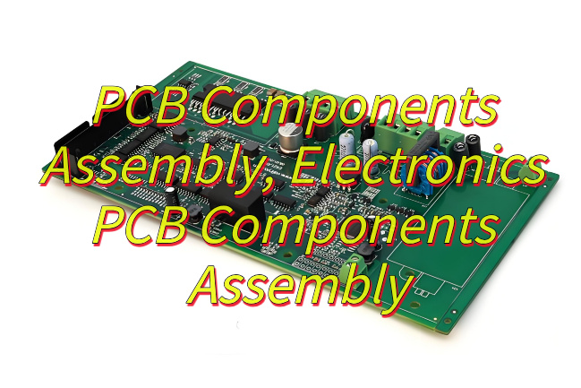
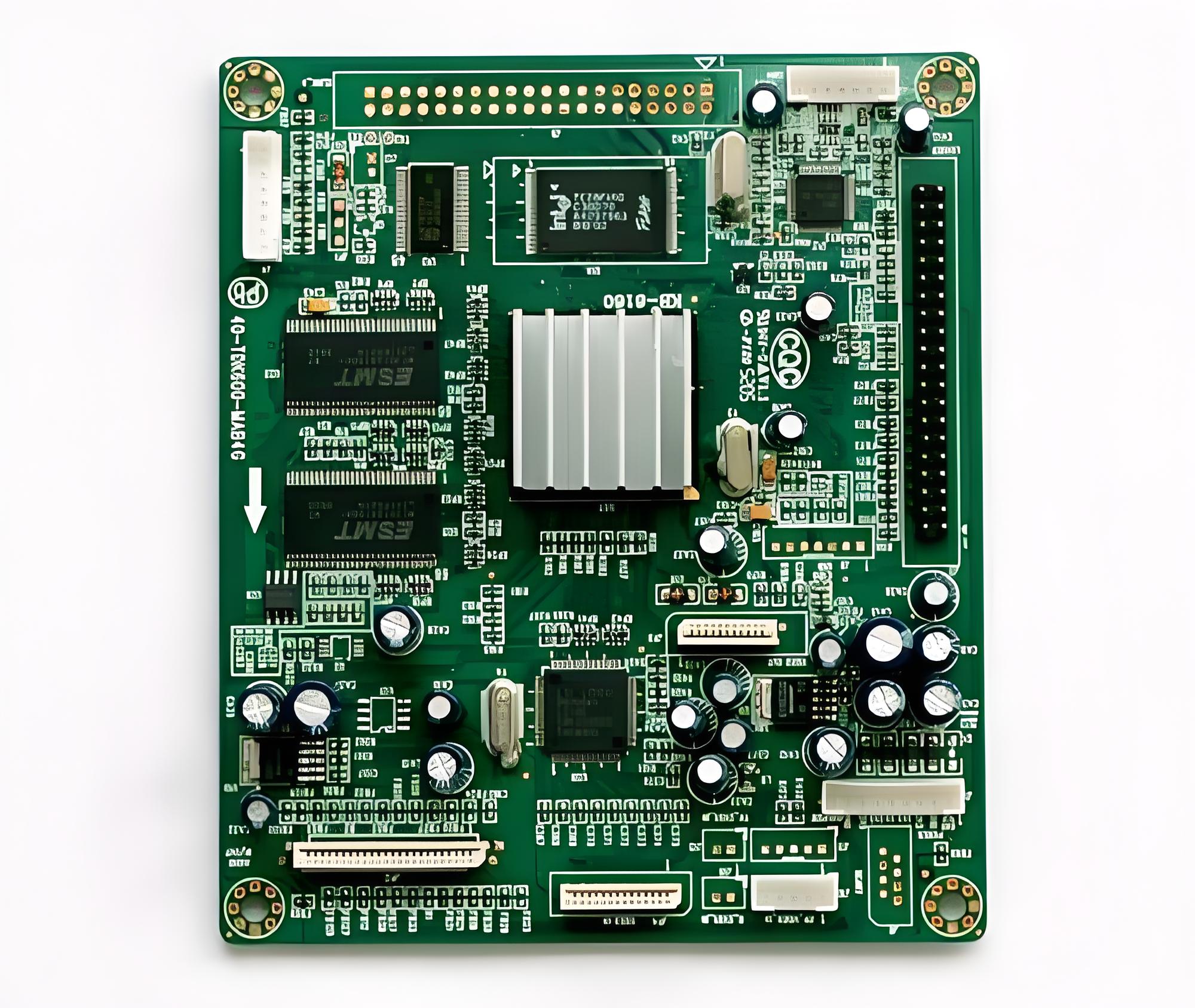
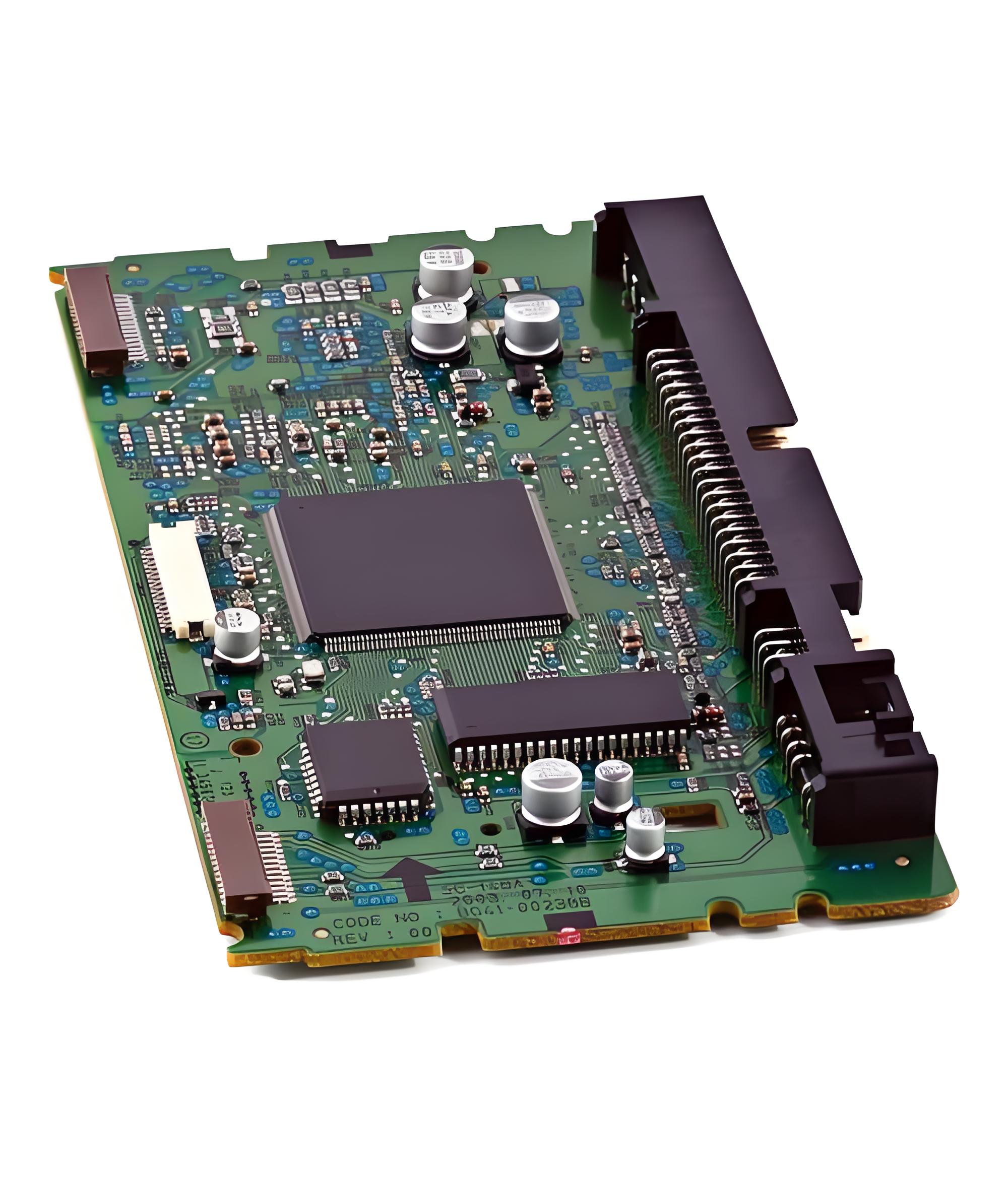
What Is PCB Components Assembly?
PCB components assembly refers to the systematic process of mounting and interconnecting electronic components onto printed circuit boards to create functional devices. This intricate procedure involves precise placement of components through surface mount technology or through-hole methods, followed by soldering processes that establish electrical connections. The PCB components assembly workflow integrates design specifications with manufacturing execution, requiring controlled environments to maintain signal integrity and thermal performance. Modern PCB components assembly techniques must accommodate miniaturized components with tolerances under 50 microns while ensuring reliability across industrial temperature ranges. The evolution of PCB components assembly continues to address challenges in high-speed digital circuits and mixed-signal systems through advanced materials and process controls.
Why Choose PCB Components Assembly?
Here are the primary reasons to choose PCB components assembly for electronic manufacturing needs:
- Precision & Reliability – PCB Components Assembly ensures accurate placement of components down to micron-level tolerances, guaranteeing consistent electrical performance and long-term durability in diverse operating conditions.
- Scalability & Efficiency – The standardized processes in PCB Components Assembly allow for high-volume production while maintaining quality, making it ideal for mass manufacturing with repeatable results.
- Advanced Technology Integration – PCB Components Assembly supports modern electronics by handling miniaturized components, high-speed signal routing, and mixed-signal designs essential for cutting-edge applications.
- Cost-Effective Production – Through optimized material usage and automated workflows, PCB Components Assembly reduces waste and labor costs compared to manual assembly methods.
- Quality Assurance Compliance – Rigorous inspection protocols in PCB Components Assembly, such as AOI and X-ray testing, ensure defect-free assemblies meeting industry standards.
- Design Flexibility – PCB Components Assembly accommodates complex layouts, multilayer boards, and specialized materials, enabling customized solutions for various technical requirements.
- Thermal & Signal Integrity Management – Controlled manufacturing environments in PCB Components Assembly prevent overheating and signal loss, crucial for high-performance devices.
What Is Process of PCB Components Assembly?
1. Material Preparation and Inspection
- The first step involves verifying the integrity of all components (resistors, capacitors, microchips, etc.) and the bare PCB. Components are checked for correct values, polarity, and physical damage. The PCB is inspected for flatness, pad cleanliness, and the absence of oxidation. This stage establishes the groundwork for error-free PCB components assembly.
2. Solder Paste Deposition
- A stainless-steel stencil, aligned with the PCB’s solder pad layout, is used to apply solder paste—a mixture of metal alloys and flux—to the board. This is typically done via a stencil printer, which ensures uniform thickness and placement. The paste’s viscosity and stencil thickness are optimized to prevent solder splattering or insufficient joints during heating.
3. Automated Component Placement
- Surface-mount devices (SMDs) are placed onto the PCB using high-precision pick-and-place machines. These machines use vacuum nozzles to transfer components from reels or trays to their designated positions. For dense boards, placement accuracy of ±0.05 mm is common. This mechanical precision is vital for the success of PCB components assembly, as even slight misalignment can cause electrical failures.
4. Reflow Soldering
- The PCB passes through a reflow oven, where controlled heating cycles melt the solder paste, bonding components to the pads. The oven’s temperature profile—including preheat, soak, reflow, and cooling phases—is calibrated to avoid thermal stress on components. For through-hole parts, wave soldering or selective soldering may follow this step.
5. Manual Insertion and Through-Hole Soldering
- Components incompatible with automated placement (e.g., connectors, electrolytic capacitors) are manually inserted into pre-drilled holes. Hand-soldering with temperature-controlled irons ensures strong joints without damaging heat-sensitive parts. This step combines human skill with automation to address complex assembly needs.
6. Automated Optical and Functional Testing
- Automated Optical Inspection (AOI) systems scan the board for defects like missing components, solder bridges, or tombstone effects. Functional tests, such as in-circuit testing (ICT) and boundary scan, verify electrical performance. These validations are essential to catch issues early, reducing rework costs in later stages.
7. Cleaning and Protective Coating
- Residual flux or contaminants are removed using ultrasonic cleaners or isopropyl alcohol. For applications exposed to moisture or vibrations, conformal coatings (e.g., acrylic, epoxy) are applied to shield the assembly from environmental stressors.
8. Final Quality Audit and Packaging
- A visual inspection confirms adherence to cosmetic standards, while X-ray or microsection analysis validates hidden solder joints. Boards passing all tests are labeled, stacked in antistatic packaging, and prepared for integration into end products.
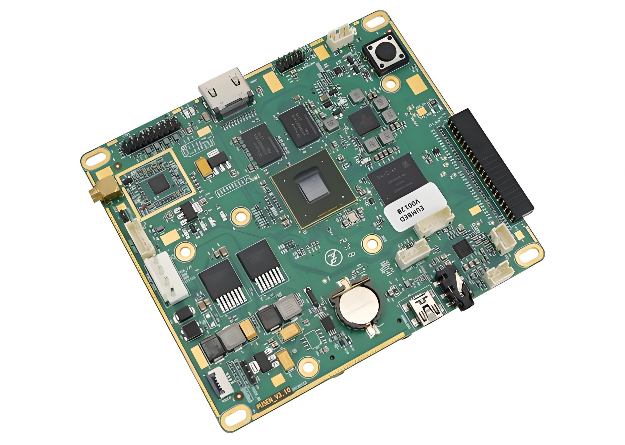
What Is Electronics PCB Components Assembly?
Electronics PCB components assembly is the manufacturing process where electronic parts are systematically mounted and interconnected on printed circuit boards to create functional electronic devices. This process encompasses multiple stages including solder paste application, precise component placement using automated machinery, and controlled soldering to establish electrical connections, with electronics PCB components assembly being particularly vital for handling modern miniaturized components down to 01005 package sizes. The reliability of electronics PCB components assembly depends on advanced techniques like reflow profiling and optical inspection to ensure proper thermal management and signal integrity in high-density layouts. As the foundation of electronic product development, electronics PCB components assembly bridges design intent with physical realization while supporting both prototyping and volume production requirements across industries.
How to Optimize the Process of Electronics PCB Components Assembly?
- Automate Repetitive Tasks With Precision Equipment – Deploy automated pick-and-place machines and solder paste printers to minimize human error in component placement and solder application. This reduces labor costs, accelerates throughput, and improves alignment accuracy for dense or miniaturized boards. Automation also ensures repeatability, critical for high-mix, low-volume production runs.
- Implement Real-Time Quality Monitoring – Integrate Automated Optical Inspection (AOI) and In-Circuit Testing (ICT) systems at critical stages (e.g., post-soldering, post-assembly). Early defect detection prevents costly rework later. For example, catching solder bridges during reflow saves time compared to debugging finished boards. Share inspection reports with clients to build transparency and trust.
- Streamline Component Sourcing and Inventory – Partner with authorized distributors to stabilize component availability and reduce lead times. Use inventory management software to track usage patterns and implement Just-in-Time (JIT) replenishment. This minimizes excess stockpiling and avoids production delays due to shortages—a common pain point for clients with tight deadlines.
- Optimize Soldering Profiles for Energy Efficiency – Customize reflow oven temperature curves based on board density and component types. Shorter ramp-up times and targeted heating zones reduce energy consumption by up to 20% without compromising solder joint integrity. Lower operational costs translate to more competitive pricing for clients.
- Adopt Modular Fixturing for Quick Changeovers – Use interchangeable jigs and pallets to reconfigure assembly lines faster between product variants. This reduces downtime during setup, enabling faster response to client requests for prototypes or urgent revisions. For instance, switching from a consumer IoT board to an automotive-grade PCB takes minutes instead of hours.
- Train Teams on Defect Prevention, Not Just Detection – Conduct regular workshops on soldering best practices, ESD control, and IPC standards. Empower technicians to halt production if systemic issues arise (e.g., misaligned stencils, skewed components). Fewer defects mean fewer rejected boards and on-time deliveries—a direct benefit to clients’ production schedules.
- Leverage Data Analytics for Process Improvement – Collect and analyze data from machines (e.g., pick-and-place cycle times, AOI defect rates) to identify bottlenecks. Use tools like Pareto charts to prioritize fixes (e.g., addressing the 10% of components causing 80% of placement errors). Continuous improvement reduces lead times by 15–30% over six months.
- Design for Assembly (DFA) With Clients Early On – Collaborate during product development to simplify designs for manufacturability. Suggest component alternatives (e.g., replacing through-hole parts with SMDs) or panelization strategies to reduce assembly steps. Proactive DFA lowers per-unit costs and accelerates time-to-market for clients.
- Implement Traceability Systems for Accountability – Use barcode scanning or RFID tags to track every board through assembly, testing, and packaging. In case of field failures, root-cause analysis becomes faster, protecting clients from warranty claims. Traceability also simplifies compliance with industry regulations (e.g., medical, automotive).
How to Ensure the Assembly Quality of PCB Components?
Below are methods about how to ensure the assembly quality of PCB components:
Strict Incoming Material Inspection
- Action: Verify components (resistors, capacitors, ICs) and bare PCBs for defects before assembly. Use automated optical inspection (AOI) and X-ray fluorescence (XRF) analyzers to confirm solderability, polarity, and moisture sensitivity levels.
- Benefit: Reduces the risk of component failures in the field, avoiding costly recalls or warranty claims.
Controlled Solder Paste Application
- Action: Calibrate stencil printers to deposit solder paste with precise volume and placement. Monitor paste height and area ratio to prevent solder bridges or insufficient joints.
- Benefit: Ensures strong, durable connections that withstand thermal cycling and vibration, extending product lifespan.
Automated Placement With Real-Time Feedback
- Action: Use high-speed pick-and-place machines equipped with vision systems to align components accurately. Implement closed-loop feedback to adjust for minor deviations during production.
- Benefit: Minimizes misalignment errors, reducing rework and accelerating time-to-market for your products.
Multi-Stage Quality Gates
- Action: Integrate AOI after soldering, followed by in-circuit testing (ICT) and functional testing. For example, AOI detects solder defects, while ICT verifies electrical continuity.
- Benefit: Catches issues early, preventing defective boards from reaching your assembly line and causing production delays.
Environmental and ESD Control
- Action: Maintain cleanroom-like conditions (ISO 7 standard) with controlled humidity (30–60% RH) and temperature. Use ESD-safe mats, wrist straps, and ionizers to protect sensitive components.
- Benefit: Prevents electrostatic discharge (ESD) damage, which can cause intermittent failures or premature product death.
Employee Training and Certification
- Action: Train technicians on IPC-A-610 standards, soldering techniques, and defect prevention. Certify operators annually to ensure adherence to best practices.
- Benefit: Skilled workers reduce human error, improving first-pass yield and lowering per-unit costs.
Traceability and Documentation
- Action: Implement barcode scanning or RFID tracking for every board and component. Retain inspection logs, test results, and calibration records for at least five years.
- Benefit: Enables rapid root-cause analysis if issues arise, protecting you from liability and ensuring compliance with regulations.
Design for Assembly (DFA) Collaboration
- Action: Partner with clients during product design to simplify layouts (e.g., avoid overly dense boards) and recommend component alternatives.
- Benefit: Reduces assembly complexity, leading to faster production and fewer design-related defects.
Destructive and Non-Destructive Testing
- Action: Conduct microsectioning to validate solder joints and cross-sections. Use X-ray inspection for hidden defects in BGA or QFN packages.
- Benefit: Provides confidence in long-term reliability, especially for high-stakes applications like automotive or medical devices.
Continuous Improvement Through Data Analytics
- Action: Analyze defect trends (e.g., 15% of reworks due to tombstone effects) using statistical process control (SPC). Adjust processes proactively.
- Benefit: Lowers defect rates over time, translating to higher profit margins and happier end-users.
How to Control the Cost of Electronics PCB Components Assembly?
Controlling costs in electronics PCB components assembly requires balancing efficiency, quality, and strategic resource management. Below is a client-focused plan to reduce expenses without compromising reliability or performance:
Automate High-Volume Tasks
- Action: Deploy automated pick-and-place machines and solder paste printers for repetitive steps like SMD placement.
- Benefit: Lowers labor costs by up to 40% and reduces errors, avoiding costly rework. Faster throughput also shortens lead times, enabling quicker time-to-market.
Optimize Component Sourcing
- Action: Consolidate suppliers for bulk discounts and negotiate long-term contracts. Prioritize standardized, widely available parts over obsolete or niche components.
- Benefit: Reduces per-unit material costs by 10–25% and minimizes supply chain risks like shortages or price hikes.
Design for Manufacturability (DFM)
- Action: Collaborate with clients to simplify PCB layouts (e.g., reduce layer counts, avoid overly dense component placement).
- Benefit: Simpler designs cut assembly time by 15–30% and lower defect rates, directly reducing production costs.
Implement In-Line Quality Checks
- Action: Use Automated Optical Inspection (AOI) and X-ray machines immediately after soldering to catch defects early.
- Benefit: Early detection reduces rework by 50% or more, avoiding the expense of fixing fully assembled boards.
Adopt Energy-Efficient Processes
- Action: Optimize reflow oven temperature profiles and switch to LED curing for conformal coatings.
- Benefit: Cuts energy consumption by 20–35%, lowering utility bills and environmental footprint.
Streamline Inventory Management
- Action: Use Just-in-Time (JIT) inventory systems and predictive analytics to order components only as needed.
- Benefit: Reduces storage costs and waste from obsolete stock, freeing up capital for other priorities.
Train Teams on Cost-Aware Practices
- Action: Educate operators on waste reduction (e.g., minimizing solder paste waste, reusing scrap PCBs for testing).
- Benefit: Lowers material waste by 10–20% and fosters a culture of continuous improvement.
Leverage Modular Fixturing
- Action: Use interchangeable jigs and pallets to reduce setup times between product variants.
- Benefit: Cuts changeover downtime by 50%, maximizing equipment utilization and reducing hourly machine costs.
Outsource Non-Core Processes
- Action: Partner with specialized vendors for secondary operations like conformal coating or box-build assembly.
- Benefit: Avoids capital investment in niche equipment and benefits from the vendor’s economies of scale.
Analyze Data for Process Improvements
- Action: Track metrics like first-pass yield, cycle time, and defect rates to identify cost-saving opportunities.
- Benefit: Targeted tweaks (e.g., reducing solder paste defects) can lower costs by 10–15% over six months.
What Is Lead Time of Electronics PCB Components Assembly?
The lead time for electronics PCB components assembly depends on multiple factors, from design complexity to production volume. Below is a breakdown of key influences and strategies to expedite the process without compromising quality:
Design Complexity and DFM Reviews
- Impact: Intricate designs (e.g., HDI boards, micro BGAs) require longer setup and testing. A design with 10+ layers may take 20–30% longer than a 2-layer board.
- Solution: Conduct Design for Manufacturability (DFM) reviews early. Simplifying layouts or replacing custom parts with off-the-shelf components can reduce lead time by 15–25%.
Component Sourcing and Lead Times
- Impact: Long-lead-time components (e.g., specialized ICs, custom connectors) can delay assembly by weeks.
- Solution: Use authorized distributors with global inventory networks. For critical parts, maintain safety stock or negotiate blanket orders to secure delivery slots.
Production Volume and Line Capacity
- Impact: Small batches (e.g., 1–100 units) may prioritize speed over efficiency, while mass production (10,000+ units) requires scaling equipment and labor.
- Solution: Optimize panelization (grouping multiple boards on a single panel) to boost throughput. Automated lines can cut lead time by 40% for large orders.
Quality Control and Testing Phases
- Impact: Multi-stage inspections (AOI, ICT, functional testing) add 1–3 days but are essential for reliability.
Conclusion
In summary, PCB component assembly is the core link of electronic product manufacturing, which requires taking into account process accuracy, efficiency and quality assurance. EBest Circuit (Best Technology) provides customers with a one-stop solution from design to mass production by integrating SMT/THT cutting-edge technology, full-process quality inspection system and customized services. We not only optimize the assembly process and strictly control costs, but also help products land quickly with industry-leading delivery speed. Whether you need prototype proofing or mass production, contact EBest Circuit (Best Technology) immediately for a professional quote and let us use our 20 years of industry experience to protect your electronic products!