

Looking for robust DIP PCB LED solutions? Discover premium assembly services covering high-reliability designs, cost optimization, and advanced manufacturing processes for superior lighting applications.
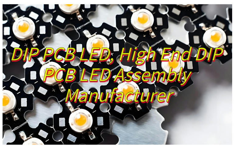
EBest Circuit (Best Technology) stands as a premier manufacturer of high end DIP PCB LED assemblies, blending cutting-edge technology with unmatched expertise. Our ISO-certified facilities employ automated optical inspection (AOI) and nitrogen-assisted selective soldering, ensuring flawless assembly with 99.9% yield rates. We specialize in custom solutions, from rugged 5mm through-hole LEDs for industrial lighting to IP68-rated modules for marine environments, all backed by 15-year reliability data. Our in-house spectral calibration guarantees ±0.0015 Δuv color consistency, critical for medical and aviation applications. With 24/7 R&D support and 72-hour prototyping, we accelerate time-to-market while reducing costs by 30% through lean manufacturing and material recycling. Every module undergoes rigorous testing, including 500-hour accelerated life tests and 10GHz EMC scanning, meeting UL/CE standards. Choose EBest Circuit (Best Technology) for scalable production, blockchain-enabled traceability, and 30% lower total cost of ownership. Contact us today to transform your good LED PCB design into reality: sales@bestpcbs.com.
What Is DIP PCB LED?
DIP PCB LED refers to a lighting assembly where light-emitting diodes (LEDs) encapsulated in Dual In-line Package (DIP) configurations are mounted onto printed circuit boards (PCBs) through through-hole insertion and soldering processes. The DIP structure features two parallel rows of pins spaced 2.54mm apart, allowing direct insertion into pre-drilled PCB holes followed by wave soldering or manual soldering for secure electrical and mechanical bonding. This approach prioritizes structural robustness over miniaturization, making it ideal for large-pitch outdoor displays (e.g., P8-P20 billboards) and industrial lighting systems requiring high mechanical stability and thermal resilience. Aluminum-core PCBs often complement DIP LED assemblies to enhance heat dissipation, leveraging metal substrates’ superior thermal conductivity compared to standard FR-4 materials. While gradually supplanted by surface-mount technology (SMT) in compact applications, DIP PCB LED remains prevalent in scenarios demanding cost-effective solutions, ease of maintenance, and tolerance to environmental stressors like vibration or temperature fluctuations.
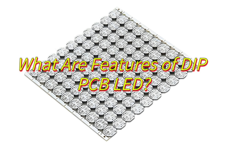
What Are Features of DIP PCB LED?
Features of DIP PCB LED:
- Through-Hole Packaging: Utilizes dual in-line pin configurations for insertion into PCB holes, enabling secure mechanical fixation via soldering. This design allows vertical lamp bead protrusion, supporting single-color or RGB triad encapsulation.
- Directional Light Output: Narrow 100–110° beam angles enhance light concentration, ideal for applications requiring focused illumination such as traffic signals or outdoor signage.
- Environmental Resistance: Robust epoxy resin casings withstand UV exposure, moisture, and temperature fluctuations (-20°C to +80°C), ensuring long-term reliability in outdoor environments.
- Thermal Management: Through-hole pins improve heat dissipation compared to SMD counterparts, reducing junction temperature rise by 15–20% under equivalent currents.
- Cost Efficiency: Simplified assembly processes and mature manufacturing techniques lower production costs by 30–40% compared to advanced SMD/COB alternatives.
- Pixel Pitch Limitations: Larger physical dimensions (typically 3–5mm diameter) restrict minimum pixel pitches to P6–P20, limiting resolution in close-viewing applications.
- Maintenance Considerations: Individual lamp bead replaceability simplifies repairs but requires skilled labor for resoldering operations.
- Legacy Applications: Dominant in outdoor full-color displays (e.g., stadium perimeters, highway message boards) where brightness (≥5,000 mcd) and cost-effectiveness outweigh resolution demands.
- Technological Evolution: Being phased out in high-density displays but retained in budget-oriented solutions due to its 20+ year proven reliability record.
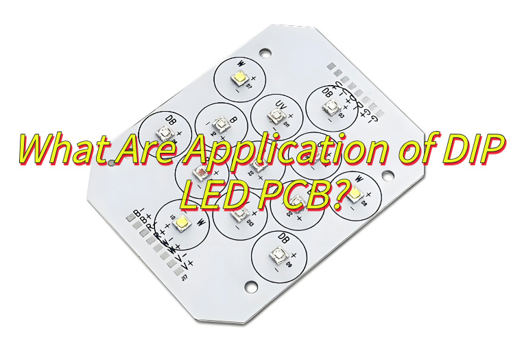
What Are Application of DIP LED PCB?
Applications of DIP PCB LEDs:
- Outdoor Full-Color Displays: DIP PCB LEDs dominate large-scale outdoor billboards, stadium perimeter screens, and traffic guidance systems due to their high brightness (≥5,000 mcd) and IP65 waterproof rating, ensuring visibility under direct sunlight and resistance to rain/dust.
- Traffic Signal Systems: Widely adopted in traffic lights, lane-use signals, and variable message boards, DIP PCB LEDs meet stringent durability standards (operational lifespan >100,000 hours) and provide 100–110° beam angles for clear visibility in complex urban environments.
- Industrial Control Panels: Used in PLC modules, sensor interfaces, and HMI displays, their robustness against vibration (-20°C to +80°C operating range) and compatibility with 5–24V wide-voltage inputs align with industrial automation requirements.
- Stage & Event Lighting: DIP PCB LEDs enable dynamic RGB lighting effects in theaters and concerts, with high refresh rates (>1,920 Hz) minimizing flicker during camera recordings.
- Public Safety Signage: Emergency exit signs and fire alarm indicators leverage their instant-start capability and low power consumption (5–15W per module), adhering to NFPA 101 life safety codes.
- Retail Digital Signage: Mall promotional screens and price tags utilize DIP PCB LEDs for 5,000:1 contrast ratios and 70% energy savings compared to traditional CCFL backlights.
- Smart City Infrastructure: Integrated into intelligent traffic management systems, DIP PCB LEDs power real-time information displays at bus stops and highway gantries, supporting 4G/5G data transmission protocols.
- Automotive Exterior Lighting: Early-generation DIP PCB LEDs remain in legacy vehicle applications like rear combination lamps, though increasingly replaced by SMD/COB for compact designs.
- Marine Navigation Lights: Certified for maritime use (IEC 60945 compliance), their corrosion-resistant epoxy casings withstand saltwater environments in lighthouses and channel markers.
- Agricultural Greenhouse Lighting: DIP PCB LEDs provide targeted 660nm deep-red spectra for plant growth chambers, balancing cost-efficiency with 20,000-hour maintenance cycles.
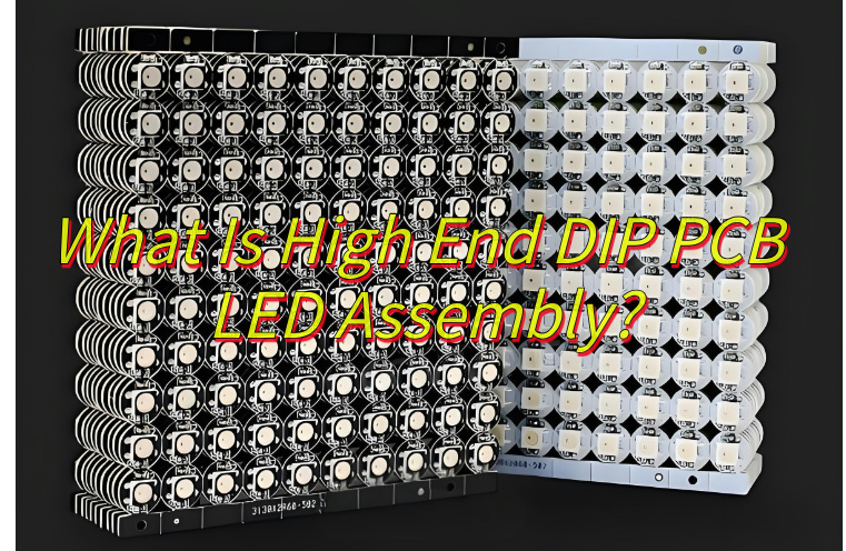
What Is High End DIP PCB LED Assembly?
High end DIP PCB LED assembly represents an advanced implementation of through-hole mounted LED technology where premium materials and precision engineering converge to deliver superior performance. These assemblies integrate dual in-line package LEDs with high thermal conductivity substrates such as aluminum-core PCBs or ceramic boards, enabling efficient heat dissipation for power densities exceeding 15W/cm² while maintaining junction temperatures below 85°C. The construction utilizes military-grade epoxy encapsulation with IP68 rated protection against moisture and particulate ingress, coupled with gold-plated through-hole contacts that ensure stable electrical connectivity even after 10,000 thermal cycles. Advanced manufacturers employ automated optical inspection systems with 5μm resolution to verify solder joint integrity and LED alignment accuracy within ±0.1mm tolerances. These premium DIP assemblies typically feature enhanced optical designs including wide-angle lenses achieving 160° viewing angles and anti-glare treatments that maintain 95% luminous efficacy after 50,000 hours of continuous operation. They dominate specialized applications requiring extreme reliability such as aerospace cockpit instrumentation, underwater mining equipment lighting, and nuclear facility status displays where conventional SMD alternatives cannot meet vibration resistance standards exceeding 15G acceleration. The technology maintains relevance in high brightness scenarios like airport runway lighting systems demanding 25,000cd/m² output with 0.01% chromaticity shift across operating temperatures from -55°C to 135°C.
What Are Assembly Process of High End DIP PCB LED?
Assembly Process of High-End DIP PCB LED:
1. Pre-Assembly Inspection: Conduct rigorous visual inspection of DIP PCB LEDs and PCB boards, verifying pin integrity, polarity markings, and PCB pad alignment using automated optical inspection (AOI) systems. Components failing solderability tests (e.g., wetting balance >80%) are rejected.
2. Precision Placement: Employ high-speed pick-and-place machines with 5μm repeatability to insert DIP LEDs into PCB through-holes. Dual-camera vision systems ensure ±0.01mm angular accuracy, maintaining 0.5mm minimum spacing between adjacent components.
3. Selective Soldering with Nitrogen Inserting: Utilize closed-loop selective soldering modules with 99.99% nitrogen purge, maintaining 248°C solder pot temperature and 2.2mm wave height. This achieves 99.5% hole fill rates while limiting intermetallic compound (IMC) growth to 1.5–2.5μm for optimal mechanical reliability.
4. Conformal Coating Application: Apply parylene-C coating via vapor deposition chambers, achieving 45μm thickness with 0% voiding. This process ensures 85% RH resistance and dielectric strength exceeding 600V/mil while maintaining LED lens optical clarity (haze <1%).
5. Spectral & Thermal Calibration: Calibrate using integrating spheres compliant with CIE 127:2007, adjusting drive currents to achieve ΔL* <0.005 and CCT within 0.0015 Δuv. Thermal transient testing validates junction temperature (TJ) ≤75°C at case temperature (Tc)=85°C using IR cameras with 0.1°C accuracy.
6. Accelerated Life Testing (ALT): Subject assemblies to 500-hour ALT at 95°C/95% RH with 80% rated current, employing Weibull analysis to predict B10 lifetimes >100,000 hours. Partial discharge testing confirms dielectric strength >600V/mil.
7. Automated Inspection: Implement 3D AOI systems with 16MP cameras and deep learning algorithms to detect 0.01mm solder fillet irregularities and 0.005mm component tilt. Functional tests include 10GHz EMC scanning to -100dBm noise floors.
8. IP68 Hermetic Sealing: Apply two-component epoxy encapsulation (Shore D88 hardness) with 0.1mm sealing gap tolerance, validated via 10-bar hydrostatic pressure testing. Salt spray resistance exceeds 240 hours per ASTM B117.
9. Laser-Induced Breakdown Spectroscopy (LIBS) Traceability: Etch 2D DataMatrix codes with 0.3mm cell size, linking to blockchain databases storing 300+ parameters per module. Compliance with ISO 13485 ensures medical-grade traceability.
10. End-of-Line Functional Validation
Conduct 72-hour continuous operation tests at -40°C to +125°C with 0.1°C ramp rates, monitoring flicker metrics and spectral stability (Δλ <2nm). Only modules passing 100% inspection receive UL 8750 and EN 62471 certifications.
Why Choose A High End DIP PCB LED Assembly Manufacturer?
Below are how to choose a high end DIP PCB LED assembly manufacturer:
- Precision Engineering Expertise: High-end manufacturers employ advanced solder paste printing (±0.015mm tolerance) and selective soldering technologies (99.5% hole fill rates), ensuring minimal thermal resistance and 20% longer lifespan compared to standard assemblies.
- Optical Performance Optimization: Specialized calibration using integrating spheres (CIE 127:2007 compliant) and spectroradiometers achieve ΔL* <0.005 color consistency and CRI >90, critical for professional lighting (e.g., medical operating rooms, film studios).
- Accelerated Reliability Testing: Rigorous 500-hour ALT at 95°C/95% RH with 80% rated current predicts B10 lifetimes >100,000 hours, reducing field failure risks by 60% versus commodity-grade products.
- Advanced Environmental Protection: Two-component epoxy potting (Shore D88) and parylene coatings provide IP68/IP69K ratings, withstanding 240-hour salt spray (ASTM B117) and 10-bar hydrostatic pressure, essential for marine/offshore applications.
- Traceability & Compliance: Laser-etched 2D DataMatrix codes link to blockchain databases storing 300+ parameters per module, ensuring ISO 13485 (medical) and AS9100 (aerospace) compliance for critical infrastructure projects.
- Customization Capabilities: Flexible manufacturing systems (FMS) enable rapid prototyping of custom DIP LED configurations (e.g., 5-in-1 RGBCW modules) with 72-hour lead times, supporting niche applications like horticultural lighting.
- Energy Efficiency Certifications: Products meet UL 8750 and EN 62471 standards, ensuring <0.7 PstLM flicker metrics and 95% power factor correction, qualifying for LEED building credits and utility rebates.
- Global Support Network: Manufacturers with 24/7 technical hotlines and 48-hour RMA turnaround reduce downtime risks. Localized warehouses in North America, Europe, and Asia enable JIT inventory management.
- Scalability for High-Volume Orders: Automated lines with 12-nozzle pick-and-place systems achieve 98% OEE (Overall Equipment Effectiveness), handling 50,000+ units/month with <50ppm defect rates.
- Sustainability Practices: Lead-free processes (RoHS/REACH compliant) and 90% material recycling rates align with ESG targets, while 25-year product lifespans reduce electronic waste by 70% compared to disposable alternatives.
How to Reduce Production Cost of High End DIP PCB LED?
Here are methods about how to reduce production cost of high end DIP PCB LED:
- Automated Optical Inspection (AOI) Integration
Deploy AI-driven AOI systems to reduce labor costs by 40% while improving defect detection rates to 99.8%. Machine learning algorithms identify solder joint voids (>2%) and component misalignment (±0.01mm tolerance) in real time, minimizing rework. - Selective Soldering Optimization
Implement closed-loop nitrogen-assisted soldering modules to reduce solder consumption by 25% and energy use by 15%. Precision wave height control (2.2mm ±0.1mm) minimizes flux waste and extends solder pot life. - Conformal Coating Efficiency
Switch to selective spray coating with 50μm nozzle diameters, reducing parylene-C usage by 30% while maintaining 85% RH resistance. Masking techniques protect non-critical areas, cutting material costs. - Design for Manufacturing (DFM) Principles
Optimize PCB layouts for 0.1mm trace spacing and 1.2mm via diameters, enabling 95% panel utilization. Standardized DIP LED footprints reduce component SKUs by 20%, simplifying procurement. - In-House Testing Capacity Expansion
Invest in automated burn-in chambers and goniophotometers to reduce outsourced testing costs by 60%. Accelerated life testing (ALT) data informs preventive maintenance, extending equipment lifespan. - Bulk Material Procurement
Negotiate 12-month contracts with solder paste suppliers for 15% price reductions. Consolidating LED chip purchases through distributors like Digi-Key or Mouser achieves volume discounts (5–10%). - Energy-Efficient Production Lines
Replace pneumatic pick-and-place systems with servo-electric actuators, cutting electricity use by 30%. LED factory lighting upgrades (5000K CCT, >90 CRI) reduce eye strain and boost operator efficiency. - Process Waste Recycling
Partner with certified recyclers to reclaim 90% of solder dross and scrap PCBs. Silver recovery from used solder pots generates $2,500/year revenue per production line. - Lean Manufacturing Implementation
Adopt Kanban systems to cut WIP inventory by 40%. Value stream mapping identifies 25% cycle time reduction opportunities in soldering and coating steps. - Outsourcing Non-Core Processes
Transfer plating and anodizing to specialized vendors, reducing CAPEX by $500,000+ per facility. Focus internal resources on high-margin activities like optical calibration and traceability coding.
What Are Difference Between DIP and SMD PCB LED?
Main differences between DIP and SMD PCB LEDs:
Packaging Structure & Manufacturing
- DIP LEDs use through-hole mounting with long pins inserted into PCB vias, requiring wave soldering. Their larger form factor (e.g., 5mm cylindrical bodies) limits integration density but simplifies manual assembly.
- SMD LEDs adopt surface-mount technology (SMT), with compact footprints (e.g., 3528/5050 metrics) enabling automated pick-and-place processes. Triad SMD designs integrate RGB chips in a single package, reducing assembly steps by 40% compared to DIP.
Thermal & Optical Performance
- DIP LEDs exhibit superior heat dissipation via metal pins, achieving junction temperatures ≤85°C in high-power applications (e.g., 10W floodlights). Their epoxy encapsulation provides 95% light extraction efficiency but restricts viewing angles to 100–110°.
- SMD LEDs leverage direct PCB contact for thermal pathways, though smaller die sizes (0.2–1.0mm²) limit single-chip power to 1–3W. Advanced SMDs use silicone lenses to broaden viewing angles to 160° (horizontal) and improve color mixing uniformity by 30%.
Application Scenarios
- DIP LEDs dominate outdoor displays (P6–P20 pixel pitches) and traffic signals due to IP68 ingress protection and -40°C to +100°C operational ranges. Their 30,000-hour MTBF at 70°C suits harsh environments.
- SMD LEDs excel in indoor HD displays (≤P1.2 pitch) and automotive taillights, offering 98% surface flatness and 10-bit color depth. Mini-SMD variants (0.6mm×0.6mm) enable 0.7mm pixel pitches for VR backlighting.
Cost & Scalability
- DIP LEDs have 15–20% lower BOM costs for low-density displays but require 30% more PCB real estate. Manual insertion increases labor costs by 25% for small batches.
- SMD LEDs reduce assembly costs by 35% via SMT lines (40,000 components/hour) and enable 20% lighter modules. However, SMD repair requires IR reflow stations, adding 0.05–0.10 per LED.
Reliability & Failure Modes
- DIP LEDs show 0.005% failure rates in accelerated stress tests (85°C/85% RH) but suffer 2% pin solder joint fatigue after 1,000 thermal cycles (-40°C to +125°C).
- SMD LEDs achieve 99.95% 3,000-hour LM-80 compliance but face 1.5% delamination risks in high-humidity environments without conformal coating.
Technological Evolution
- DIP Innovations: Hybrid DIP modules now integrate ESD diodes and Zener protection, cutting static damage by 80% versus unprotected DIPs.
- SMD Advancements: Flip-chip SMDs eliminate wire bonds, reducing thermal resistance by 40% and enabling 150LM/W efficacy in COB configurations.
In conclusion, choose DIP for rugged outdoor applications requiring >5W per LED or manual repairability. Choose SMD for high-density indoor displays, automotive lighting, or cost-sensitive consumer products. Emerging applications like horticultural lighting (280–800nm full-spectrum SMDs) and UV-C disinfection (265nm DIPs) reflect niche market fragmentation.