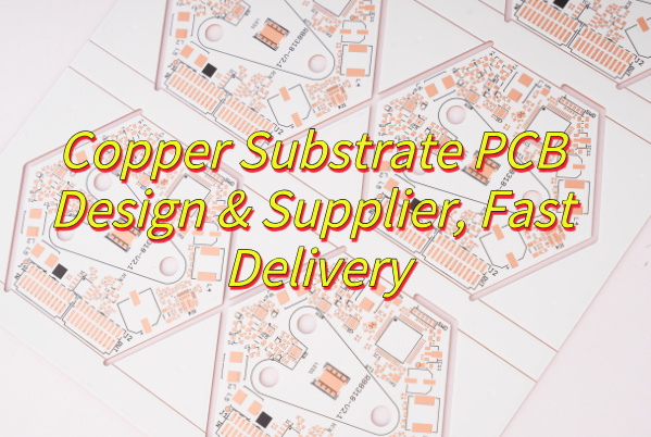
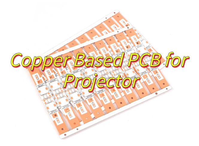
Why choose copper based PCB for projector? Let’s explore definition, benefits, design guide and manufacturing process, case study for copper based PCB.
Are you still troubled by these issues?
- Why do traditional PCBs flicker at high brightness?
- Why are cooling fans becoming increasingly noisy?
- Why are repair costs so high?
EBest Circuit (Best Technology) offers copper substrate solutions:
- Services: Custom copper-based PCB thermal conductive layers, with thermal conductivity reaching up to 398W/m·K.
- (The copper layer directly connects to the bottom of the LED driver chip, dissipating 90% of heat in 0.3 seconds and improving image stability by 65%).
- Services: Embedded copper block + micro-hole array design.
- (A 2oz thickened copper layer combined with a 0.4mm heat dissipation hole array reduces thermal resistance to 0.4°C/W and reduces fan speed by 40%).
- Services: Anti-oxidation surface treatment for copper substrates.
- (Nickel-gold plating on the copper layer, salt spray resistance exceeding 500 hours, extending device life to 50,000 hours).
Welcome to contact us if you have any request for copper based PCB: sales@bestpcbs.com.
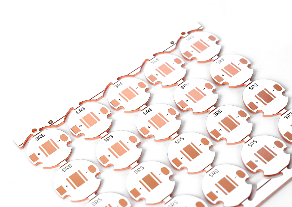
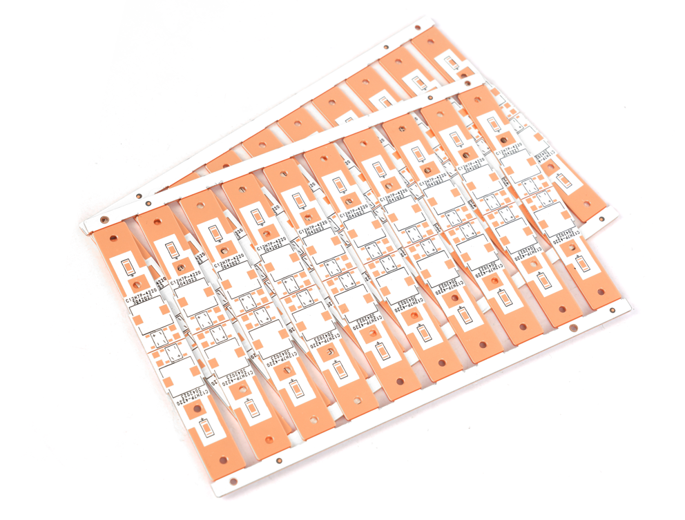
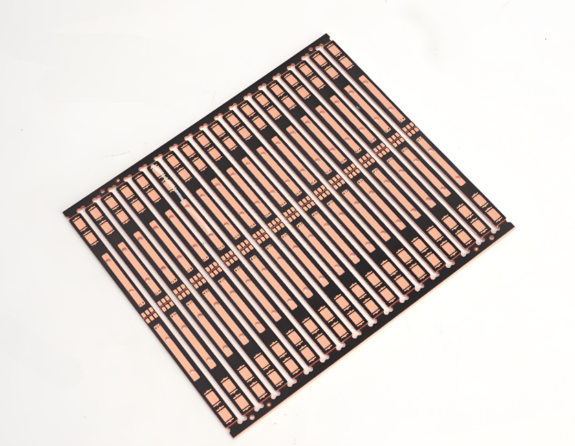
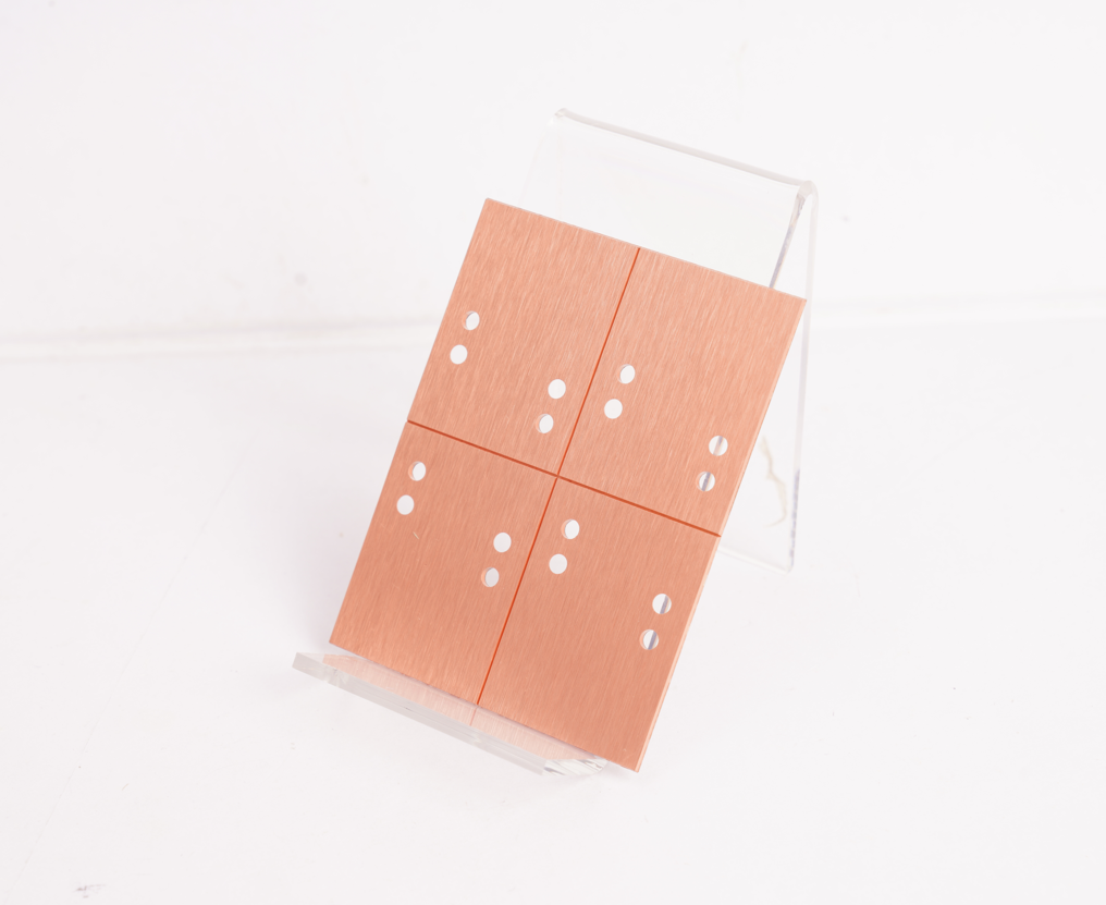
What Is Copper Based PCB?
Copper based PCB (also called copper substrate PCB) is a printed circuit board with a copper core layer designed for superior thermal conductivity. It efficiently dissipates heat from high-power components in applications like LEDs, power supplies, and projectors, outperforming traditional FR4 boards. The copper core (typically 0.5-3.0mm thick) ensures reliable performance in thermally demanding environments.
Why Choose Copper Based PCB for Projector?
- Superior Heat Dissipation: Copper core (300-400 W/m·K) efficiently transfers heat away from high-power LEDs/Laser diodes, preventing thermal throttling and extending projector lifespan.
- Compact & Lightweight: Enables thinner projector designs (0.5-3.0mm thick) without sacrificing cooling performance, ideal for portable and home theater systems.
- Reliable Performance: Stable operation under continuous high-power loads (50W+), reducing flickering risks and maintaining consistent brightness.
- Cost-Effective Longevity: Lower maintenance costs due to reduced thermal stress on components, minimizing failures and warranty claims.
- Industry Standard for High-Brightness Models: Trusted by top projector brands for 4K/ultra-short-throw models demanding rigorous thermal management.
How to Design a Projector Copper Based PCB?
1. Requirements Analysis and Planning
- Defining Parameters: Determine projector power (e.g., 300W LED light source), size (e.g., compact size ≤ 200mm²), heat dissipation requirements (temperature rise ≤ 85°C), and EMC standards (e.g., CISPR 32).
- Material Selection: Select the copper substrate type (single-sided/double-sided/multi-layer) and thickness (1.0-3.0mm). Use high-thermal-conductivity PP material (0.1-0.3mm thickness) for the insulation layer.
2. Schematic Diagram and Layout Design
- Modular Layout: Divide modules by function (e.g., light source driver, signal processing). Heat-generating components (LEDs, laser diodes) are concentrated at the board edges, utilizing the copper substrate edges for heat dissipation.
- Core Component Positioning: Prioritize placement of the DMD chip and laser light source, ensuring precise alignment with the optical components (error ≤ 0.1mm).
3. Thermal Design and Simulation
- Copper Thickness Step Design: Use a 3-4oz copper layer in the core heat-generating area, tapering to 2oz at the periphery. A teardrop-shaped transition (angle ≤ 45°) is used to reduce thermal stress.
- Via Array Optimization: Arrange 0.3mm diameter heat dissipation vias (density ≥ 4 vias/cm²), combined with heat pipes (diameter 1.5mm) or phase change materials to enhance local heat dissipation.
- Simulation Verification: Use ANSYS Icepak to simulate heat distribution, ensuring hotspot temperature rise ≤ 15°C, and adjust via placement and copper thickness.
4. Signal and Power Design
- High-Speed Signal Routing: HDMI/VGA signal lines should be short and straight, avoiding 90-degree corners. Use serpentine routing to compensate for delays (differential line length error ≤ 5 mil).
- Power Distribution: Separate power and ground planes, with ground trace widths ≥ power lines (e.g., 10A power trace width ≥ 2mm). Critical signals (such as clocks) should be ground-wrapped, and return vias should be added when switching differential signal layers.
5. Manufacturing and Assembly Considerations
- Drilling Specifications: Hole diameters should meet the board thickness ratio (≤ 10:1) to avoid drill contamination, and depth-to-aperture ratios ≤ 0.8:1.
- Surface Treatment: Use immersion gold (Immersion Gold) (Ni thickness 3-5μm, Au 0.05-0.1μm) to prevent deformation of the copper substrate caused by tin spraying.
- Machining: Milling is used for copper substrate cutting, with edge chamfers of 0.8-1mm and a ≥2mm keep-out zone around the screw holes.
6. Verification and Testing
- DRC Check: Ensure there are no shorts or opens, and that line widths and spacing meet manufacturing capabilities (e.g., minimum line width 0.1mm).
- Prototype Testing: Test thermal performance (temperature rise ≤ 85°C), signal integrity (eye diagram test), and mechanical strength (vibration test).
How to Make a Projector Copper Based PCB?
1. Cutting and Pretreatment
- Substrate Cutting: The raw copper substrate (double-sided or single-sided) is cut into production panels according to the designed dimensions, with a typical thickness of 1.0-3.0mm.
- Edge Treatment: The board edges are processed using an automatic edge grinder and corner filleter to remove burrs and chamfer the edges by 0.8-1mm.
- Cleaning and Baking: The board surface is cleaned to remove oxide layers and contaminants, and then baked at a high temperature (120-150°C) to relieve stress.
2. Inner Layer Circuit Fabrication
- Pretreatment: Chemical cleaning of the copper surface is performed to increase roughness and improve dry film adhesion.
- Dry Film Lamination: A photosensitive dry film (15-25μm thick) is applied by hot pressing to cover the copper surface.
- Exposure and Development: UV exposure is used to transfer the circuit pattern, and a developer (1% Na₂CO₃) is used to remove the uncured dry film.
- Etching: An acidic copper chloride solution is used to etch the exposed copper areas, forming the inner layer circuits. The line width tolerance is ≤±10%.
- Film Stripping and Inspection: A strong alkaline solution is used to remove the protective dry film, and AOI is used to inspect for circuit defects (shorts, opens).
3. Lamination and Heat Dissipation Enhancement
- Brown Treatment: Chemically roughens the copper surface of the inner layer to enhance interlayer bonding.
- Lamination and Lamination: The layers are stacked in the order of “copper foil – prepreg (PP) – inner layer – PP – copper foil” and pressed using a vacuum laminator (temperature 180-200°C, pressure 30-50 kg/cm²).
- Heat Dissipation Vias: Laser drilled (hole diameter 0.3mm, density ≥ 4 holes/cm²), electroplated with copper (20-25μm) on the hole walls, and filled with thermally conductive silicone.
- Copper Block Embedding: T-shaped copper blocks (2.5mm thick) are embedded in the high-heat zone, ensuring 100% contact with the light source module.
4. Outer Layer Circuitry and Plating
- Outer Layer Dry Film: Repeat the inner layer process, attach the dry film, and expose and develop, leaving the areas to be plated.
- Electroplating Thickening: The copper layer is thickened to the designed thickness (e.g., 2oz in the HDMI signal area), and tin is simultaneously plated to protect the pads.
- Etching and Tin Stripping: Etching removes unprotected copper, and then using a tin stripping solution to remove the tin layer, exposing the complete outer layer circuitry.
5. Solder Mask and Surface Treatment
- Solder Mask Printing: Screen-print solder mask ink (primarily green) to cover non-solderable areas.
- Curing: UV exposure cures to retain the solder mask layer, followed by high-temperature baking (150°C) for hardening.
- Surface Treatment: Immersion Gold (5μm Ni, 0.1μm Au), with key pads locally thickened to 0.2μm.
6. Forming and Inspection
- Outer Fabrication: PCB contours are cut using a CNC milling machine, and panels are separated using a V-cut assembly.
- Electrical Testing: Flying probe testing is used to check connectivity and insulation resistance.
- Final Inspection: Visual inspection or AOI inspection is performed to check appearance (e.g., ink misalignment, board warping), ensuring compliance with IPC-A-600 standards.
7. Packaging and Shipping
- Vacuum Packaging: Vacuum-sealed in anti-static bags to prevent oxidation.
- Test Report: Includes thermal distribution diagrams, signal integrity data, and reliability test results (such as a 500-hour burn-in test).
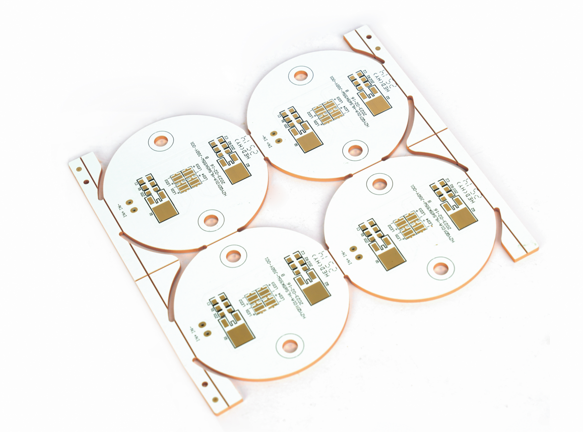
Our Projector Copper Based PCB Case Studies
At EBest Circuit (Best Technology), we have accumulated 19 years expertise in manufacturing projector copper-based PCBs, having successfully delivered multiple high-end projects for global clients. With a focus on thermal management, mechanical precision, and signal integrity, our solutions have resolved critical challenges such as high-power LED/laser heat dissipation, PCB deformation control, and ultra-high-definition signal transmission (e.g., 4K/8K HDMI 2.1). Each case applies customized copper-layer thickness zoning, embedded thermal structures, and advanced surface finishes, ensuring devices meet rigorous performance and reliability standards. This is a projector copper base PCB case we made before for your reference:

Attached is specification for this case:
| Parameter | Specification |
| Substrate Type | Double-Sided Copper |
| Copper Foil Thickness (Light Source Area) | 3oz (105μm) |
| Copper Foil Thickness (Signal Area) | 1oz (35μm) |
| Insulation Material | High-Performance Polypropylene (Thermal Conductivity: 3.0W/m·K) |
| Insulation Thickness | 0.2mm |
| Substrate Thickness | 2.0mm |
| Heat Dissipation Vias | 0.3mm Diameter, 6 Holes/cm², Filled with Thermally Conductive Silicone |
| Embedded Copper Block | T-Shaped Copper Block (2.5mm Thickness), 100% Contact Area |
| Surface Finish | Immersion Gold (Ni: 5μm, Au: 0.1μm) |
| Key Pad Thickening | Localized 0.2μm Au Layer |
| Machining | 2mm Screw Hole Keepout Area, 1mm Edge Chamfer |
Why Choose EBest Circuit (Best Technology) as Copper Based PCB Supplier?
Reasons why choose us as copper based PCB supplier:
- 19+ Years Industry Experience: Leverages proven expertise to navigate high power projector. Stringent Quality Certifications (ISO9001, ISO13485, and IATF16949): Ensures product consistency and compliance with global standards.
- Custom Thermal Management Solutions: Optimize Thermal Management and extending projector lifespan and reliability.
- Competitive Pricing: Affordable pricing without compromising quality, ideal for cost-sensitive projects.
- 24 Hours Rapid Prototyping: Accelerates time-to-market, meeting urgent production demands.
- Free DFM (Design for Manufacturability) Service: Identifies design flaws early, reducing rework costs and delays.
- Strict Quality Control – 100% automated optical inspection (AOI) for bulk orders.
- Reliable Supply Chain – Stable material sourcing to avoid delays and ensure consistency.
- Full Turnkey Solution –Providing one-stop services from design to delivery, integrating materials, processes and thermal management technologies to ensure high heat dissipation performance and reliability while significantly reducing supply chain complexity and project risks.
Our Copper Substrate PCB Capabilities
| Items | Technical Parameters |
| Product model | Copper Based |
| Copper trace thickness | 1OZ, 2OZ, 3OZ, 4OZ, up to 10OZ |
| Thermal Conductivity | 1.0, 1.5, 2.0, 3.0W/m.K |
| Surface finishing | HAL(LF)/ Gold Immersion/ Gold plating/ OSP/ Immersion Tin/ Silver Immersion |
| Soldermask Color | White/Black/Green/Blue/Red/Yellow |
| Layers | 1L, 2L, 4L, 6L, 8L, double sided, COB |
| Maximum dimension | 1,100mm*480mm; 1,500x300mm |
| Minimum dimension | 5mm*5mm |
| Minimum Line width/space | 0.1mm/0.1mm |
| Warp and twist rate | ≤0.75%(thickness:1.6mm, measurement:300mm×300mm) |
| Board Thickness | 0.3-4.5mm |
| Die-Punching dimension tolerance | ±0.15mm |
| V-cut positioning tolerance | ±0.1mm |
| Manufacturing capability | 6000m2 |
| Wall Cu thickness | 15-25um |
| Alignment tolerance | ±0.076mm |
| Minimum diameter of die-punching hole | Thickness <=1.0mm: 1.0mm |
| Thickness 1.2-3.0mm: 1.5mm | |
| Thickness 4.0mm: 2.0mm | |
| Minimum size the square groove/slot/cutout | Thickness <=1.0mm: 0.8mm×0.8mm |
| Thickness 1.2-3.0mm: 1.0×1.0mm | |
| Thickness 4.0mm: 1.5×1.5mm | |
| Outline Tolerance | CNC routing:±0.1mm; Die-punching:±0.15mm |
| Minimum diameter of hole | 0.3mm; not limit for maximum diameter of hole |
| Surface Finishing Thickness | gold plating:Ni 2.5-5um, Au: 0.025-0.075um |
| immersion gold: Ni 3-6um, Au: 0.025-0.1um | |
| HAL(LF): 3-30um | |
| V-cut Angle tolerance | ±5° |
| V-cut Range | 0.3mm-4.5mm |
| Smallest silkscreen height | 0.15mm |
| Smallest PAD | 0.1mm |
How to Get a Quote for Your Copper Based PCB?
Materials to be submitted:
- Design Documents: Gerber files, BOM, 3D structural drawings (with mechanical dimensions).
- Technical Parameters: Copper foil thickness zoning (e.g., 3oz for the light source area), insulation layer thermal conductivity (≥3.0W/m·K), surface treatment requirements.
- Special Requirements: Thermal via density, copper block size, high-speed signal impedance control (±10%).
- Order Information: Quantity (batch/sample), delivery time.
Contact EBest Circuit (Best Technology) now and submit your material list to get a quote: sales@bestpcbs.com.