PCB manufacturing PCB manufacturing
Home > Blog

Posts Tagged ‘Copper Clad PCB’

What is a Copper Clad PCB? Copper Clad Laminate (CCL)
Thursday, August 21st, 2025

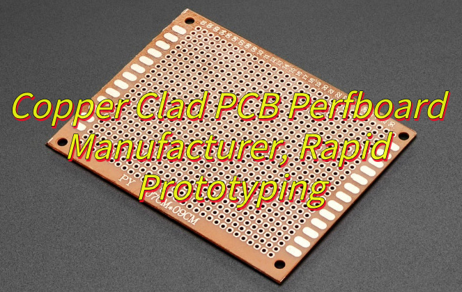
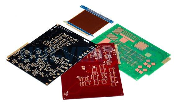
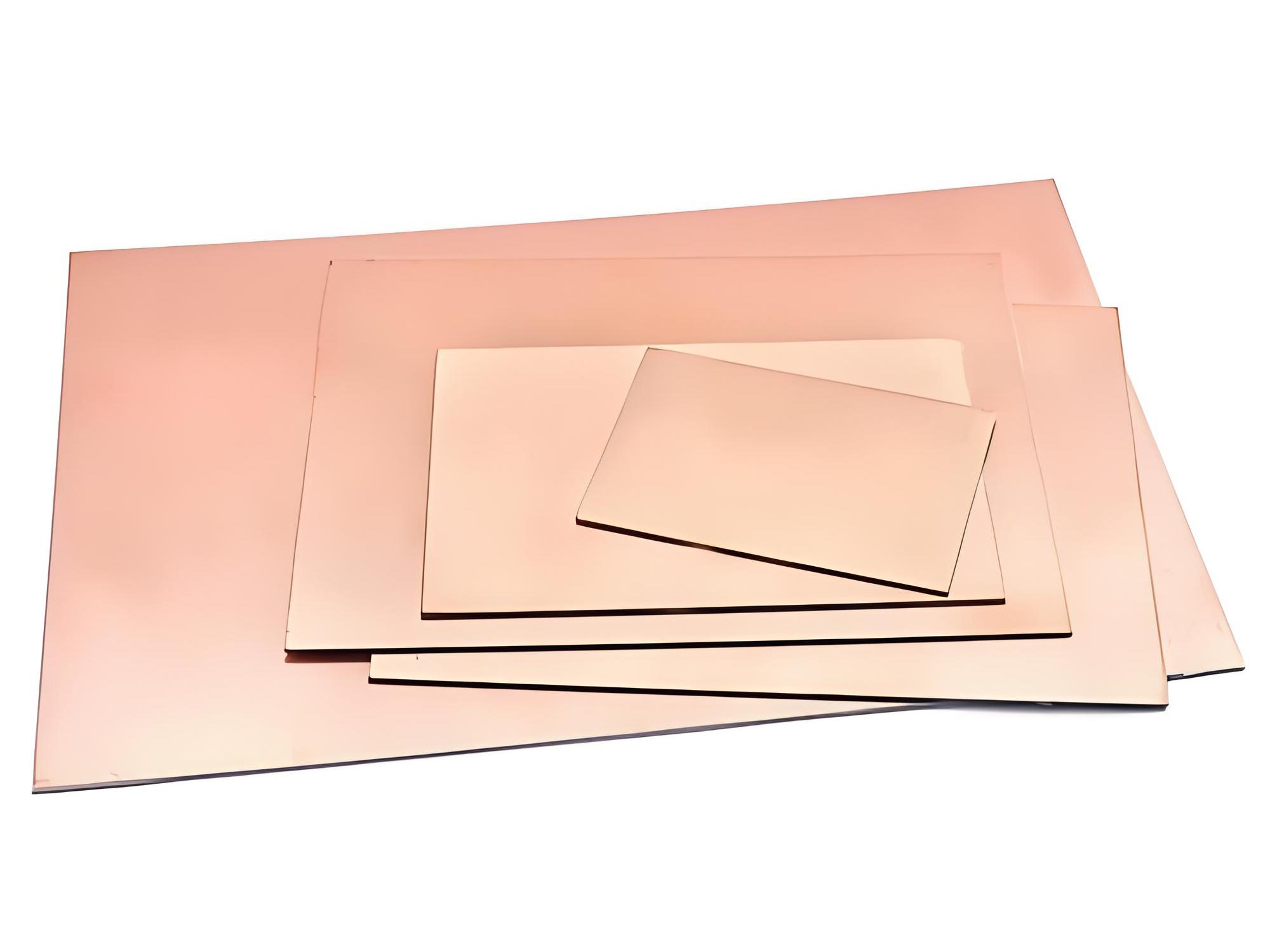
Copper clad PCB are a core material for printed circuit boards (PCBs). Composed of an insulating substrate and copper foil, these materials are heat-pressed to form a composite. They both support components and provide conductive circuits. Depending on the substrate, these materials can be categorized as paper, fiberglass, composite, or metal. They are widely used in consumer electronics, communications, automotive, and industrial control applications.

What is a Copper Clad PCB? Copper Clad Laminate (CCL)

Are you curious about Best Technology’s copper clad PCBs?

  • Does the insulation performance meet circuit insulation requirements?
  • Can the material strength withstand the processing and usage environment?
  • Is the performance and cost balance balanced?
  • Does BEST Technology provide customization and after-sales support?

Best Technology’s copper clad PCB can answer these questions.

  • Compatible. Supports standard sizes and customized specifications (thickness, shape), adapting to different PCB design requirements, and enabling fast response for small batches.
  • Performance. The base material is highly resistant to bending and impact, and can withstand cutting, drilling, and other processing processes, preventing cracking or deformation after long-term use.
  • Achieve. Performance meets industry standards, with over 100 board options for cost optimization, balancing reliability and affordability.
  • Provide. Supports customization of materials, specifications, and processes. After-sales service includes rapid response and warranty services, and expedited orders ship within 24 hours.

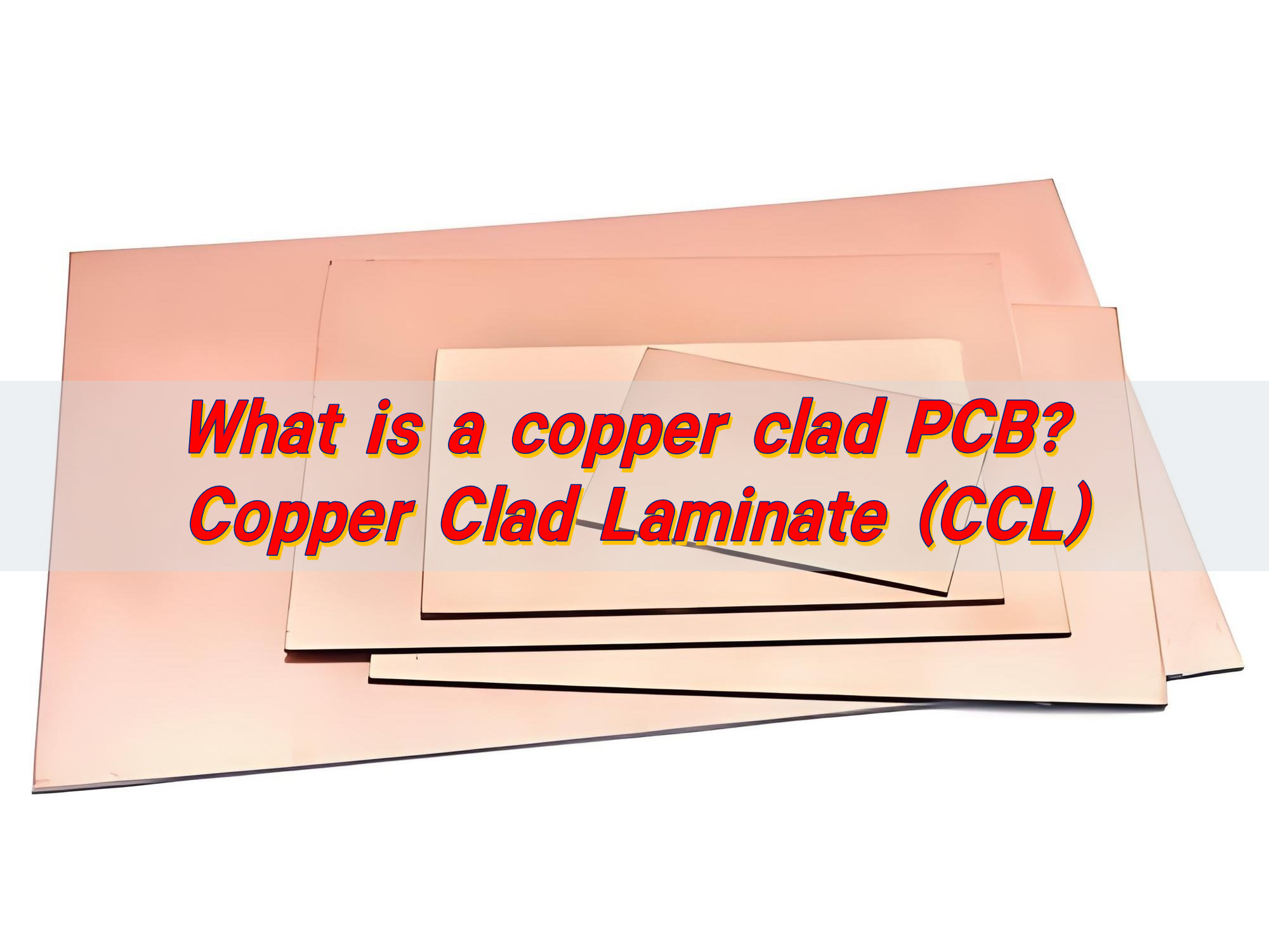
What is copper clad in PCB?

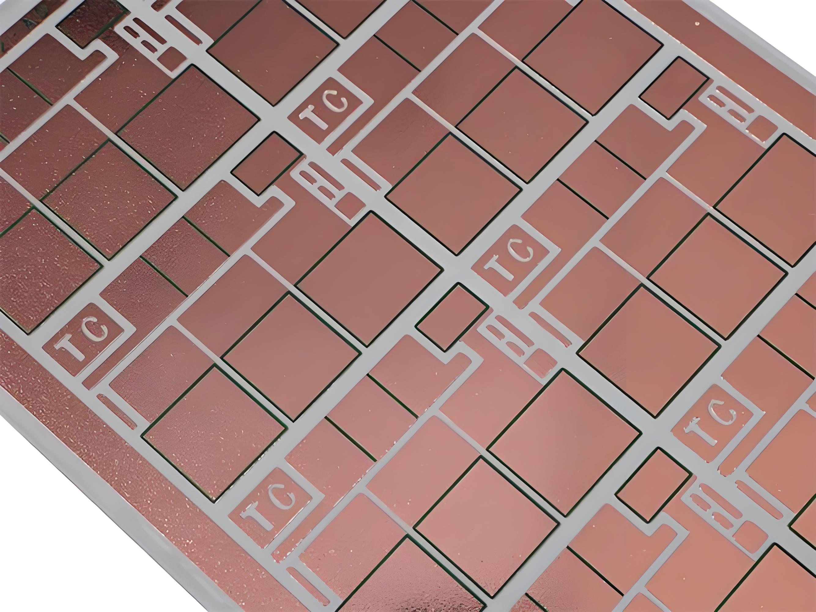
Copper clad PCB refers to a board where a thin layer of copper foil is bonded to one or both sides of a substrate, usually fiberglass or other insulating material. This copper layer forms the conductive surface where circuit patterns are later etched.

Without this copper cladding, a PCB would just be an insulator with no ability to carry signals. By laminating copper onto the substrate, the board gains electrical conductivity and becomes the foundation for electronic circuits.

The copper clad board is then processed through techniques like imaging, etching, and drilling to create pathways that allow electricity to flow between components.

In short, a copper clad PCB board is the starting point for almost every PCB. It bridges the gap between insulating materials and conductive pathways.

How thick is PCB copper clad?

Copper thickness is one of the most critical specifications in any copper clad PCB sheet. It directly affects current-carrying capacity, heat dissipation, and durability.

The thickness of copper in PCBs is usually measured in ounces per square foot (oz/ft²). Here’s what it typically looks like:

  • 0.5 oz/ft² copper → about 18 microns thick
  • 1 oz/ft² copper → about 35 microns thick
  • 2 oz/ft² copper → about 70 microns thick
  • 3 oz/ft² and above → heavy copper, often used for power electronics
What is a Copper Clad PCB? Copper Clad Laminate (CCL)

Standard consumer electronics often use 1 oz copper. High-power applications may need 2 oz or more to handle higher currents without overheating.

So, when choosing a PCB copper clad board, thickness depends on your circuit’s power requirements and performance needs.

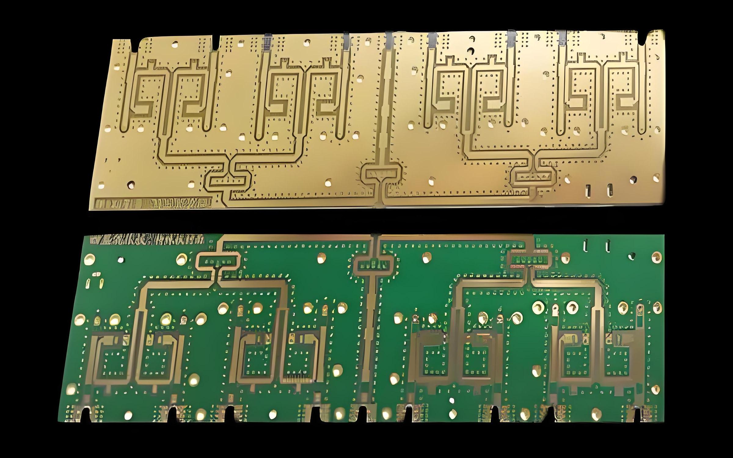
What are the materials of copper clad laminate (CCL)?

The copper clad laminate (CCL) is not just copper. It’s a composite material made of multiple layers. Each one has a specific role.

Here are the primary materials used:

1. Copper Foil

  • Conductive layer
  • Provides the pathways for current flow
  • Usually treated to improve adhesion

2. Resin System

  • Often epoxy or modified epoxy
  • Acts as a binder
  • Provides mechanical strength

3. Reinforcement Material

  • Fiberglass cloth is the most common
  • Ensures dimensional stability
  • Improves heat resistance

4. Additives

  • Flame retardants
  • Fillers for mechanical stability
  • Special compounds for high-frequency applications

The combination of these elements gives the copper clad laminate PCB its strong insulation, mechanical toughness, and long-term reliability.

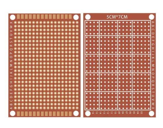
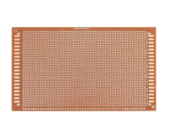
What is a PCB with copper clad on only one side called?

PCB with copper laminated on only one side is known as a single-sided copper clad board. It’s the simplest form of PCB copper clad laminate.

These are widely used in low-cost and less complex electronic devices. For example:

  • Calculators
  • Power supplies
  • LED lighting modules
  • Consumer gadgets

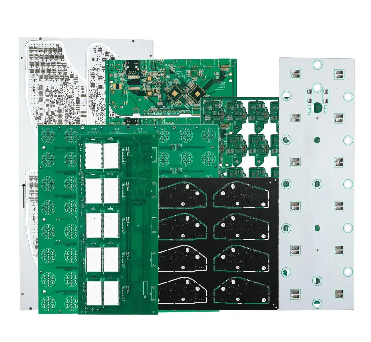
On the other hand, a double sided copper clad PCB board has copper foil on both sides. This allows more complex designs and higher component density.

Therefore, depending on the complexity of the circuit, a single-sided or double-sided option can be chosen.

What are the types of copper clad laminate (CCL)?

Copper clad laminates are available in different types to suit varied applications. Here are the main categories:

What is a Copper Clad PCB? Copper Clad Laminate (CCL)

Based on Substrate

  • Paper-based (phenolic resin) → Affordable, good for household appliances
  • Glass fabric (epoxy resin) → More durable, widely used in general electronics
  • Composite CCL → A mix of paper and fiberglass

Based on Copper Foil

  • Electrolytic copper foil → Smooth surface, ideal for precision circuits
  • Rolled annealed copper foil → Excellent ductility, used in flexible PCBs

Based on Application

  • General-purpose CCL → Cost-effective and widely used
  • High-frequency CCL → Designed for RF and microwave devices
  • High-speed CCL → Used in data communication systems
  • Thermal conductive CCL → Great for LED and power devices

Each type of copper clad laminate PCB material is designed to handle unique performance demands.

Why use a copper clad PCB board?

Copper clad PCBs bring several advantages that make them a preferred choice:

  • Excellent Conductivity: Copper provides stable and reliable current flow.
  • Thermal Management: Thicker copper spreads heat efficiently, preventing damage.
  • Mechanical Strength: Fiberglass reinforcement adds stability.
  • Design Flexibility: Available in single, double, or multilayer forms.
  • Cost Efficiency: Paper-based and FR4 laminates reduce manufacturing costs.

These advantages have led to the widespread use of copper clad PCBs in consumer electronics, automotive systems, and medical devices.

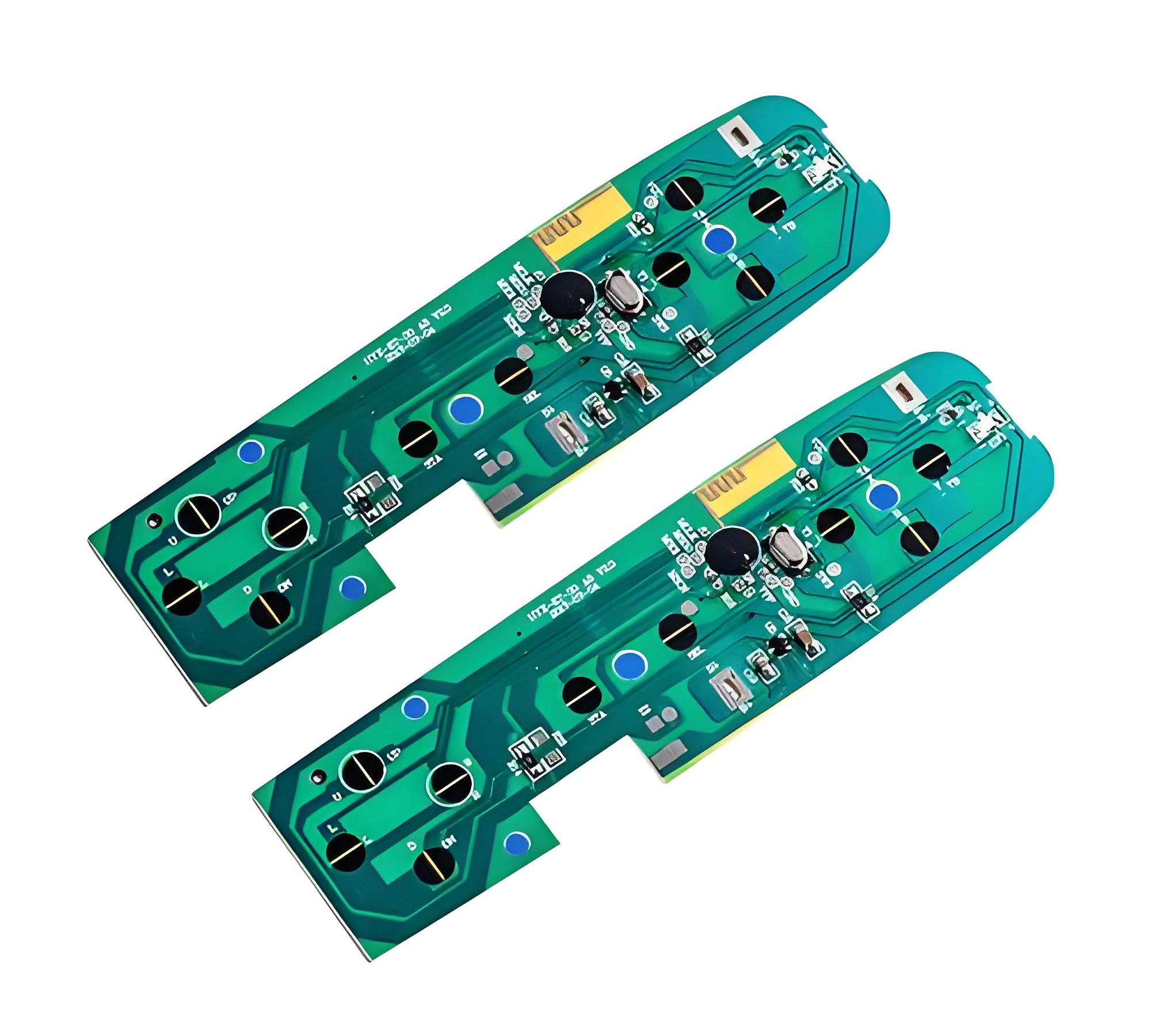
What is copper clad used for?

Copper clad boards serve as the base for many electronic products. Some key applications include:

1. Consumer Electronics

  • Smartphones, tablets, laptops
  • Wearable devices

2. Automotive Electronics

  • Control modules
  • Safety systems
  • Infotainment units

3. LED Lighting

  • High thermal conductivity versions
  • Used in LED lighting aluminum substrates

4. Industrial Control Systems

  • Robust designs for high current
  • Suitable for harsh environments

5. Medical Devices

  • Compact and reliable circuits
  • Long-term performance stability

In short, copper clad PCBs are used anywhere reliable electronic connections are required.

How to choose a copper clad board for PCB?

Choosing the right copper clad laminate PCB requires balancing performance, cost, and application needs. Here’s how you can decide:

What is a Copper Clad PCB? Copper Clad Laminate (CCL)

1. Power Requirements

  • High current? Choose thicker copper.
  • Low power? Standard 1 oz copper is enough.

2. Frequency Performance

  • For RF or high-speed circuits, select low-loss laminates.
  • For simple circuits, FR4 is cost-effective.

3. Thermal Demands

  • LEDs and power devices benefit from thermal conductive laminates.

4. Design Complexity

  • Single-sided for simple devices.
  • Double-sided or multilayer for complex designs.

5. Budget Considerations

  • Paper-based laminates are cheaper.
  • Glass-fiber laminates offer longer life.

By considering these factors, you can select the best copper clad board PCB for your project.

At Best Technology, we specialize in PCB copper clad laminates that meet international standards and deliver long-term reliability. If you are seeking a trustworthy supplier for your copper clad PCB boards, our team is here to help. Contact us today at sales@bestpcbs.com

Copper Clad PCB Perfboard Manufacturer, Rapid Prototyping
Wednesday, July 30th, 2025

Looking for copper clad PCB perfboard solutions? Let’s discover its components, functions, applications, production process, solder process and clean methods.

Are you troubled with these problems?

  • Is traditional PCB performance degradation due to poor heat dissipation?
  • Is manual soldering inefficient and resulting in poor product consistency?
  • Low-volume production costs and long lead times?

Best Technology can provide service and solution:

  • High-thermal-conductivity copper substrate: Utilizing a patented metal substrate, heat dissipation efficiency is increased by 50%, ensuring stable operation of high-frequency circuits.
  • Standardized pre-drilled design: Precise 2.54mm hole spacing combined with copper plating simplifies the soldering process and increases product yield by 30%.
  • Customized service: 24-hour sample delivery supports flexible small-batch production, reducing customer trial-and-error costs.

Feel free to contact us if you have any request for metal core PCB: sales@bestpcbs.com.

What Is Copper Clad PCB Perfboard?

Copper Clad PCB Perfboard‌ (also known as ‌veroboard‌ or ‌stripboard‌) is a type of printed circuit board (PCB) substrate with a pre-drilled grid of holes (typically spaced 2.54mm apart) and a layer of copper foil bonded to one or both sides of an insulating base material (such as fiberglass or phenolic resin). It is designed for ‌prototyping and experimental circuits‌, allowing components to be manually soldered to the copper traces and interconnected via jumpers. The copper layer provides ‌conductive pathways‌ for electrical connections while the perforations enable ‌flexible routing‌ without requiring complex PCB fabrication processes. It is widely used in ‌low-to-medium complexity projects‌ due to its simplicity and cost-effectiveness

What Is Copper Clad PCB Perfboard?

Components of Copper Clad PCB Perfboard

  • Base Material‌: Typically ‌fiberglass (FR-4)‌ or ‌phenolic resin‌, providing mechanical support and insulation.
  • Copper Foil‌: A thin layer of ‌electrodeposited or rolled copper‌ bonded to one or both sides of the base material for conductive traces.
  • Perforated Holes‌: Pre-drilled holes (usually ‌2.54mm spacing‌) for component insertion and interconnections.
  • Solder Mask (Optional)‌: A protective coating over copper traces to prevent oxidation and short circuits.
  • Silkscreen (Optional)‌: Printed markings (e.g., component labels, polarity symbols) for assembly guidance.
  • Tooling Holes‌: Used for alignment during PCB fabrication or mounting.

Functions of Copper Clad PCB Perfboard

  • Prototyping‌ – Enables quick circuit testing without complex PCB manufacturing.
  • Educational Use‌ – Ideal for learning soldering and basic circuit design.
  • Temporary Wiring‌ – Supports jumper connections for experimental setups.
  • Component Mounting‌ – Provides a stable base for mounting electronic components.
  • Custom Circuit Assembly‌ – Allows flexible hand-wired connections for unique designs.
  • Heat Dissipation (Aluminum Version)‌ – Some variants improve thermal management.
  • Cost-Effective Testing‌ – Eliminates the need for expensive PCB fabrication in early stages.
  • Repairability‌ – Circuits can be easily modified or debugged.
Functions of Copper Clad PCB Perfboard

Applications of Copper Clad PCB Perfboard

  • Prototyping & Development – Used for rapid circuit testing before mass production, allowing quick iterations.
  • Educational Purposes – Ideal for electronics students to learn soldering and circuit design hands-on.
  • DIY Electronics Projects – Popular among hobbyists for building custom circuits (e.g., amplifiers, sensors).
  • Repair & Modification – Helps fix broken PCB traces or adapt existing circuits with manual rewiring.
  • Low-Volume Production – Suitable for small-batch or one-off electronic assemblies where cost matters.
  • RF & Analog Circuits – Used in simple RF modules and analog designs due to copper’s conductivity.
  • Mechanical Enclosure Wiring – Acts as a backplane for wiring complex machinery or control panels.
  • Temporary Circuit Boards – Serves as a non-permanent solution for exhibitions or demo setups.

How to Make A Copper Clad PCB Perfboard?

Copper Clad PCB Perfboard Manufacturing Processes

1. Material Preparation

  • Base Material Selection: Typically made from fiberglass-reinforced epoxy resin (FR-4) or phenolic paper, chosen for durability and thermal resistance.
  • Copper Foil Lamination: A thin layer of copper (usually 1 oz or 2 oz thickness) is bonded to one or both sides of the base material under heat and pressure.

2. Photolithography (Optional for Custom Designs)

  • Photoresist Application: A light-sensitive coating is applied to the copper surface.
  • Exposure & Development: UV light exposes the photoresist through a mask, followed by chemical development to create circuit patterns.

3. Etching

  • Chemical Etching: Unwanted copper is removed using ferric chloride or ammonium persulfate, leaving the desired traces.
  • Rinsing & Drying: The board is thoroughly cleaned and dried to prevent residue.

4. Drilling

  • Hole Creation: Precision drilling forms holes for component leads, often using CNC machines for accuracy.
  • Deburring: Sharp edges are smoothed to avoid damage during assembly.

5. Surface Treatment

  • Plating (Optional): Gold or tin plating may be applied for corrosion resistance and solderability.
  • Solder Mask (Optional): A protective layer is added to prevent short circuits.

6. Cutting & Finishing

  • Sheet Cutting: The large panel is cut into individual perfboards.
  • Edge Profiling: Rounded or beveled edges are added for safety.

7. Quality Control

  • Electrical Testing: Continuity and insulation tests ensure functionality.
  • Visual Inspection: Checks for defects like scratches or incomplete etching.

8. Packaging

  • Anti-Static Protection: Boards are wrapped in conductive foam or bags.
  • Labeling: Batch numbers and specifications are marked for traceability.
How to Make A Copper Clad PCB Perfboard?

How to Solder Copper Clad PCB Perfboard?

1. Tools Required

  • Use a temperature-controlled soldering station (350-400℃) to prevent component damage.
  • Select 0.8-1.2mm rosin-core solder wire for optimal flow.
  • Prepare fine-tip tweezers, desoldering pump, and flux (optional).

2. Pad Preparation

  • Lightly abrade copper pad surfaces with fine sandpaper or steel brush to remove oxidation.
  • Apply minimal flux to enhance solder adhesion (thoroughly clean residue in humid environments).

3. Tinning Component Leads

  • Dip component leads into solder for 1-2 seconds to form a thin coating.
  • Avoid excess solder to prevent short circuits between adjacent pads.

4. Soldering Process

  • Secure components: Hold leads with tweezers, position soldering iron at 45° to pad/lead junction.
  • Feed solder within ≤3 seconds; achieve conical, shiny joints (rework cold joints immediately).
  • Use “drag soldering” for multi-lead components (e.g., ICs) to improve efficiency.

5. Inspection & Correction

  • Visually verify solder joints for full coverage, no cold joints, or bridges.
  • Test conductivity with multimeter; resolve shorts with desoldering braid.
  • Clean flux residues using isopropyl alcohol-soaked swabs.

6. Safety Notes

  • Work in ventilated areas; wear safety goggles.
  • Use ESD wrist straps for static-sensitive components (e.g., MOSFETs).
  • Allow 24 hours post-soldering before power-on testing to avoid latent cold joints.

How to Clean Copper Clad PCB Perfboard?

1. Tools & Materials

  • Isopropyl alcohol (≥90%), cotton swabs, soft-bristle brush (e.g., toothbrush).
  • Flux remover spray (for heavy residues), ultrasonic cleaner (optional).
  • Distilled water, anti-oxidation spray (e.g., clear lacquer).

2. Initial Surface Cleaning

  • Dip brush in isopropyl alcohol; gently scrub copper pads to remove flux/rosin.
  • Use cotton swabs for tight spaces (e.g., between component legs).

3. Stubborn Residue Removal

  • Apply flux remover spray; let sit 10-15 seconds.
  • Brush vigorously, then wipe with lint-free cloth.

4. Oxidation Treatment

  • Mix 5% citric acid solution (water-based); soak board 2-3 minutes.
  • Scrub oxidized areas with brush, then rinse thoroughly with distilled water.
  • Avoid strong acids (e.g., muriatic acid) to prevent copper erosion.

5. Drying & Protection

  • Blow-dry with compressed air or let air-dry 24 hours (avoid heat guns).
  • Apply anti-oxidation spray in thin layers; cure per product instructions.

Copper Clad PCB Perfboard Manufacturer – Best Technology

Reasons why choose Best Technology as copper clad PCB perfboard manufacturer:

  • 19-Year Metal Substrate Expertise: Avoid costly design iterations with battle-tested thermal management solutions.
  • Strict Quality Control: 100% AOI/X-ray inspection ensures flawless delivery, eliminating rework risks.
  • 24-Hour Prototyping: Your Benefit: Cut product validation time by 50% and accelerate market entry.
  • ISO 9001/14001 Certified: Global regulatory compliance simplified for seamless international sales.
  • Competitive Pricing: Achieve 20%+ cost savings through optimized production scaling.
  • Precision Manufacturing (Âą0.05mm): Enable miniaturized designs for IoT/wearable devices with reliable accuracy.
  • Custom Thermal Management: Optimize heat dissipation for high-power applications (e.g., automotive, LED).
  • Flexible MOQ (1pcs–100K+): Reduce inventory risks with agile small-batch to mass-production transitions.
  • Dedicated Engineering Support: Solve technical challenges proactively, shortening R&D cycles by 30%.

Welcome to contact us if you have request for copper clad PCB: sales@bestpcbs.com.

What are double sided FR1 circuit boards? & FR1 vs FR4
Friday, March 7th, 2025

Double Sided FR1 Circuit Boards are a type of printed circuit board (PCB) made of FR1 material with two layers of conductive traces. FR1 is a flame retardant material made of paper base and phenolic resin, with good electrical properties and cost-effectiveness, suitable for a variety of electronic devices.

What are double sided FR1 circuit boards? & FR1 vs FR4

As a PCB manufacturer with more than 18 years of manufacturing experience, BEST Technology has accumulated rich experience and excellent technical strength in the production of double-sided FR1 circuit boards. BEST Technology’s production process uses advanced equipment and a strict quality control system to ensure that each circuit board meets high quality standards.

What are double sided FR1 circuit boards?

A double-sided FR1 PCB is made from Flame Retardant 1 (FR1) material, a paper-based phenolic laminate that serves as the board’s substrate. The defining characteristic of double-sided PCBs is their copper layers on both sides, allowing components to be soldered on both surfaces.

This feature enables denser circuit layouts, making double-sided FR1 PCBs ideal for applications where single-layer boards cannot provide enough space for circuit traces.

However, because FR1 is not as heat-resistant as FR4, it is mainly used in low-power electronic devices that do not generate excessive heat.

What is the difference between FR1 and FR4 PCB?

FR1 and FR4 are two different types of PCB materials, each suited for specific applications. Here’s how they compare:

Material Composition:

  • FR1: Made of phenolic resin and paper-based material.
  • FR4: Constructed from woven fiberglass and epoxy resin, making it more rigid and durable.
What are double sided FR1 circuit boards? & FR1 vs FR4

Thermal Resistance:

  • FR1: Has a lower heat tolerance, making it unsuitable for high-temperature applications.
  • FR4: Withstands higher temperatures, ideal for demanding environments.

Durability & Strength:

  • FR1: More brittle, making it prone to cracking under stress.
  • FR4: Has high mechanical strength, suitable for multilayer PCBs.

Cost:

  • FR1: Cheaper, making it ideal for cost-effective projects.

FR4: More expensive but offers better longevity.

Common Uses:

  • FR1: Found in household electronics, small gadgets, and simple power circuits.
  • FR4: Used in industrial, automotive, and high-performance electronic devices.

What is FR1 FR2 and FR3?

Many PCB materials exist, but FR1, FR2, and FR3 are closely related. All are paper-based but with different properties:

  • FR1: Phenolic resin impregnated kraft paper substrate, with the highest heat resistance (UL 94 V-0/V-1) among the three, used for single-layer boards and basic double-sided boards (lighting equipment, home appliance control boards), with the lowest cost but poor moisture resistance and low dimensional stability.
  • FR2: Phenolic resin paper-based material, with lower heat resistance than FR1 (UL 94 V-2), mainly used for low-cost single-layer PCBs (remote controls, toy circuits), with high flammability and requiring fireproof coating and not suitable for high temperature environments.
  • FR3: Epoxy resin impregnated paper-based material, with significantly improved moisture resistance, suitable for basic consumer electronics circuits (mobile phone chargers, small home appliances), as a compromise between FR2 and FR4, but with limited high temperature resistance.

What is the difference between single-sided and double-sided PCBs?

Single-sided PCB: Copper is only coated on one side (commonly used FR1/FR2 paper-based materials), made by simple etching process, with low manufacturing cost but limited design flexibility, and complex connections require jumper wires.

Double-sided PCB: Copper is coated on both sides and uses via interconnection technology (mostly using FR3/FR4 substrates), supports double-sided layout of components and multi-layer wiring. The manufacturing cost is higher but the reliability is significantly improved.

How to make double sided FR1 circuit boards?

Manufacturing double-sided FR1 PCBs involves several steps:

  • Material preparation: Double-sided copper-clad FR1 phenolic paper substrate is selected. Its heat resistance (UL 94 V-0/V-1) and cost balance characteristics are suitable for basic double-sided board requirements.
What are double sided FR1 circuit boards? & FR1 vs FR4
  • Circuit design: Use tools to complete the Gerber file, focus on optimizing the via distribution and copper foil thickness (usually 35Îźm), and ensure that the mechanical strength of the FR1 substrate is stable during the etching process.
  • Photoresist and etching: Double-sided negative photosensitive dry film is coated, and after exposure and development, a resist pattern is formed, and the circuit is etched out using a solution.
  • Drilling and metallization: CNC drilling machine processes through holes, chemical copper plating combined with electroplating copper achieves double-sided conduction, and the FR1 substrate needs to be pre-impregnated to enhance the bonding strength.
  • Solder mask and silk screen printing: Screen printing thermosetting solder mask ink forms a protective layer, and character logos are printed at the same time.
  • Assembly and testing: Wave soldering or manual soldering of components, ICT testing after flying probe test of conductivity, FR1 board needs to avoid long-term use in high temperature environment.

What are the advantages of double sided FR1 circuit boards?

Double-sided FR1 PCBs offer several benefits:

  • Cost-Effective: One of the most affordable PCB options, making it ideal for budget-sensitive projects.
  • Lightweight: FR1 is lighter than FR4, making it easier to handle.
  • Good Electrical Insulation: The phenolic resin provides stable electrical performance.
  • Efficient for Simple Electronics: Works well in basic circuit designs, power supplies, and consumer electronics.

What are the disadvantages of double sided FR1 circuit boards?

While FR1 PCBs are useful, they have some drawbacks:

  • Lower Heat Resistance: Can degrade in high-temperature environments.
  • Brittle: More fragile than FR4, leading to possible breakage under mechanical stress.
  • Limited Multilayer Capability: Unlike FR4, FR1 does not support complex multilayer stacking.
  • Moisture Absorption: Can absorb moisture over time, affecting durability.

What are the applications of double sided FR1 circuit boards?

Due to its affordability and reliability, double-sided FR1 PCBs are widely used in:

  • Consumer Electronics: Found in TV remote controls, LED drivers, and power strips.
What are double sided FR1 circuit boards? & FR1 vs FR4
  • Power Supplies: Used in low-power voltage regulators and adapters.
  • Automotive Electronics: Found in basic control modules for car accessories.
  • Industrial Control Systems: Used in low-complexity automation circuits.

Conclusion:

Double sided FR1 circuit boards offer an affordable and efficient solution for various electronic applications. Their dual-layer design allows for more compact circuit layouts. While FR1 PCBs may have some limitations, they remain a cost-effective choice for many projects.

At BEST Technology, Whether you need double-sided FR1 PCBs or other custom PCB solutions, we are here to help. Contact us today at sales@bestpcbs.com to discuss your project needs!