

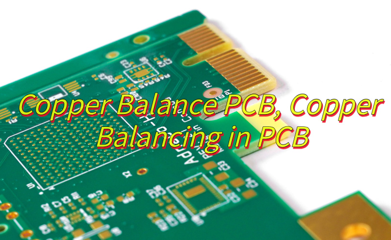
What is copper balance PCB? Let’s explore its technical parameter, purpose, application, design guide and plating uniformity optimization solutions.
Are you troubled with these problems?
- How can we ensure signal stability with uneven copper holes? (copper balance PCB heat dissipation and balanced plating)
- How can we prevent poor soldering due to interlayer deviation? (copper balance PCB rigidity and deformation prevention)
- How can we accurately control high-frequency impedance fluctuations? (copper balance PCB temperature drift suppression)
EBest Circuit (Best Technology) can provide solutions:
- Customized electroplating parameters improve copper hole uniformity by +40%
- 3D simulation predicts interlayer deviation risks
- Dynamic compensation technology achieves impedance tolerance of ±5%
Welcome to contact us if you have any request for copper balance PCB: sales@bestpcbs.com.
What is Copper Balance PCB?
A copper balance PCB( also called copper balancing in PCB) requires symmetrical distribution of copper traces and coverage within each layer of the PCB stackup, ensuring consistent copper weight and thickness on the top and bottom layers (or within each inner layer). This is similar to a mirror image design, where the top and bottom layers are perfectly symmetrical to prevent mechanical stress caused by differences in thermal expansion coefficients. For example, during the CAD design phase, engineers create new layers (such as Layer 0 for the board outline and Layer 1 for top-side copper traces) and calculate copper areas to ensure even coverage on both sides.
Copper Balance PCB Technical Parameters
| Technical Parameter | Specifications |
| Copper Thickness Range | Inner Layers: 0.5-3oz (17-105μm) |
| Outer Layers: 1-4oz (35-140μm) | |
| Symmetry Tolerance | Layer-to-Layer Copper Distribution Deviation ≤5% |
| Fill Pattern | Low-Density Areas: Solid Blocks (≥5mm²) |
| High-Density Areas: Mesh Grids (0.3-0.8mm Pitch) | |
| Current Density | Inner Layers: 1.2-1.8A/ft² |
| Outer Layers: 0.8-1.2A/ft² (With Thieving Dots) | |
| Minimum Feature Size | Isolated Copper Dots: Diameter ≥50μm |
| Mesh Lines: Width/Spacing ≥80μm | |
| Thermal Stress Resistance | After 3× Thermal Cycles (-40°C~125°C), Warpage ≤0.5% |
| Impedance Control Differential Pair | ±5Ω Tolerance |
| Single-Ended Trace | ±8% Tolerance |
| DFM Validation Methods | 3D Field Solver for Copper Distribution Analysis; IPC-2221A Current Density Check |
Purpose of PCB Balancing Copper
- Preventing PCB board twisting, bending, or warping: Symmetrical copper trace distribution reduces mechanical deformation caused by differences in thermal expansion coefficients, ensuring a flat board and avoiding manufacturing defects and assembly issues.
- Reducing ground impedance and voltage drop: Balanced copper coverage reduces ground resistance and stabilizes current flow, thereby reducing noise interference and improving power efficiency.
- Reducing the risk of internal track fracture: Even copper distribution helps dissipate heat and stress, preventing damage to internal tracks caused by thermal stress or mechanical pressure.
- Optimizing signal transmission and reducing interference: Copper foil filler improves interference immunity, improves signal integrity, and reduces high-frequency signal coupling and noise.
- Enhancing thermal management: Copper acts as a heat dissipation layer, effectively conducting heat, eliminating the need for additional heat sink components, reducing manufacturing costs and the risk of thermal stress.
- Increasing structural strength and reliability: Balanced copper increases the thickness of conductors and pads, ensuring strong connections between layers and improving the mechanical durability of the board.
Applications of Copper Balance PCB
- LED street lights and traffic lights
- Automotive lighting (headlights/taillights)
- Surgical shadowless lamps and camping lights
- Engine power controllers
- Electric vehicle chargers and inverters
- Servo motor drive circuits
- Arc welder power modules
- Solar inverters and UPSs
- Textile machinery driver boards
- CT/X-ray scanner heat sinks
- Surgical lighting systems
- 5G base station filters
- Server power modules
- Airborne radar modules
- Hi-fi audio amplifiers
- Smartphone motherboards
Difference between Copper Balance vs Copper Thieving in PCB
| Dimension | Copper Balancing | Copper Thieving |
| Core Objectives | Prevent physical deformation (warping, twisting) | Ensure plating uniformity (copper thickness, impedance consistency) |
| Application Layer | Inner layers only | Outer layers only |
| Added Elements | Non-conductive copper blocks (large-area fill) | Isolated copper geometries (dots, squares, etc.) |
| Key Risks | Lamination voids, thermal stress fractures | Over-etching (mushroom pads), impedance abrupt changes |
| Design Constraints Requires | interlayer symmetric distribution | Must keep away from signal lines & impedance control areas |
How to Achieve Copper Balancing in PCB?
Here are ways about how to achieve copper balancing in PCB:
1. Core Principles of Copper Balancing
- Ensure symmetric copper distribution across PCB layers to prevent warping (max deviation <0.7% thickness).
- Maintain impedance consistency (±5% tolerance for high-frequency designs).
2. Implementation Methods
Mirror Stack Design
- Symmetrical copper coverage (top/bottom layers deviation <5%).
- Central layers (e.g., L3/L4 in 6-layer boards) should have thicker copper to distribute stress evenly.
Dynamic Plating Control
- Pulse plating adjusts via copper thickness (40% uniformity improvement for blind vias).
- Monitor plating solution (60–80g/L Cu²⁺, 50℃±1℃).
Copper Pour Optimization
- Use grid copper (spacing λ/20) in non-routing areas to avoid resin flow issues.
- Avoid sharp corners (radial edges minimize EMI).
3. Quality Validation
- Mechanical Test: Post-reflow warpage ≤0.3mm/m (288℃, 3 cycles).
- Electrical Test: 10GHz impedance variation ≤±2Ω.
- Microscopic Analysis: Uniform copper grain size (≤5μm via SEM).
4. Case Studies
- HDI Board: BGA cracking due to 18% copper imbalance fixed by prepreg compensation (reduced to 3%).
- Aluminum Base PCB: Overheating resolved via stepped copper design (3oz in high-heat zones).
5. Special Considerations
- Thick Copper Boards (≥3oz): Staged lamination (120℃/50PSI → 180℃/250PSI).
- Flexible PCBs: Low-temperature bonding (160–200℃) with flexible adhesives.
Copper Balance PCB Design Guideline
1. Copper Thickness Selection
- A 1oz (35μm) base copper thickness is preferred for standard boards. Power layers and high-current paths can be partially thickened to 2oz.
- Multilayer boards require interlayer copper balance: the difference in copper foil area between adjacent layers should be ≤10% to prevent warping caused by thermal lamination.
2. Copper Foil Distribution Principle
- Ground and power layers should use solid copper fill (Solid Pour) to reduce impedance and improve heat dissipation.
- Signal layers should use grid copper fill (Grid Pour) to balance interlayer compressive stress.
3. Tracking Rules
- Bend traces at 45° angles; avoid 90° right angles (to reduce reflections and space waste).
- Critical signal trace widths should be ≥0.2mm. Power trace widths should be calculated based on current (Tool: PCB Trace-Width Calculator).
- A 10% margin should be reserved for high-frequency signals to compensate for etching tolerances.
4. Via and Copper Connections
- Annular rings on through-hole pads should be ≥0.15mm. Microvias should be ≥0.05mm.
- Avoid unnecessary vias and prioritize blind and buried vias to optimize high-density routing.
5. Symmetrical Lamination Design
- PCBs with four or more layers should use a symmetrical stackup (e.g., Top-GND-PWR-Bottom). The core board thickness tolerance should be ±10%.
- The thicknesses of the copper and dielectric layers must match the coefficient of thermal expansion (CTE) to avoid delamination.
6. Heatsink Copper Area Treatment
- Independent copper heatsinks should be provided beneath high-power devices to connect multiple vias to the internal ground plane.
- Coordinate the opening ratios of the copper foil and solder mask to avoid localized overheating.
7. Design Checklist
- Use Design for Manufacturing (DFM) tools to verify copper balance: inter-layer copper area ratio, minimum trace spacing, and aperture ratio.
- Perform electrical rule checking (ERC) and design rule checking (DRC) before submitting process files.
8. Vendor Collaboration Requirements
- Confirm the PCB manufacturer’s process capabilities (e.g., minimum trace width/maximum copper thickness) in advance.
- Indicate special requirements (e.g., impedance control layer, ±10% copper thickness tolerance).
9. Design Document Annotation
- Reference identifiers (R1/C2) should be placed away from densely populated areas to avoid obstruction.
- Net names should be named according to their function (e.g., VCC_3V3, GND_DIGITAL).
- Add a laminate diagram and indicate the copper thickness of each layer.
Copper Balance PCB Plating Uniformity Optimization Solution
Current Density Control
- Forward pulse (100–200ms, 40–60A/dm²) + reverse pulse (5–10ms, 6–10A/dm²) reduces via-to-surface thickness ratio from 1:2.5 to 1:1.2, improving yield to 98.5%.
- Adjust edge current density by 15–20% to minimize “edge effect” (edge plating thickness ≤ 1.8× center).
Plating Solution Improvement
- Accelerator (4-amino-2-thiophene carboxylic acid, 40–60ppm) increases via-bottom deposition rate by 35%.
- Leveler (heterocyclic quaternary ammonium salts, 20–30ppm) reduces surface copper growth by 50%.
- Copper sulfate (60±5g/L), sulfuric acid (100±10g/L), temperature (50±1℃) reduces roughness (Ra) by 50%.
Equipment & Fixture Optimization
- Optimize titanium basket positioning: Adjust bottom screen by 2mm reduces bottom thickness variation by 4%; adjust side screen by 20mm reduces CoV from 7.0% to 5.1%.
- Use conformal anodes for complex boards, improving current distribution uniformity by 25%.
Spray System Calibration
- Pressure gradient: 15–20% lower at edges reduces thickness variation by 35%.
- Intermittent spray eliminates “bath effect,” improving uniformity by 40%.
Pre-Treatment & Process Control
- Micro-etching (Ra 0.8μm) improves adhesion from 0.8N/cm to 1.5N/cm.
- Strict degreasing (<0.5mg/cm² residue) reduces plating defects by 35%.
Real-Time Monitoring
- Online bath composition control: Metal ion variation ±3%, additives ±5%.
- Temperature control (50±0.5℃) improves uniformity by 15%.
Design Optimization
- Copper distribution error ≤5% (≤8% for inner layers), reducing warpage by 30%.
- Avoid isolated copper areas (<0.5mm²; fill or remove if necessary).
High-Density Zone Compensation
- Differential pairs: +10% current reserve reduces impedance variation from ±15% to ±3%.
- Laser vias (0.1mm) with pulse control: Height variation <0.2μm.
Quality Verification Standards
- CoV (Coefficient of Variation): ≤10% (optimized to 5.1%).
- Range method: ≥90% (requires high-end chemicals & rectifiers).
Reliability Testing
- Thermal cycling (−55℃ to 125℃, 1000 cycles): No delamination; thick copper (≥3oz) improves bend strength by 150%.
- Peel strength: Electrolytic copper ≥1.5N/mm, rolled copper ≥2.0N/mm.
Conclusion
To sum up, the above content is all about technical parameter, purpose, application, design guide and plating uniformity optimization solutions for copper balance PCB. If you have any other issues about copper balance PCB, please feel free to contact us: sales@bestpcbs.com. Looking forward to hearing from you soon!