PCB manufacturing PCB manufacturing
Home > Blog

Posts Tagged ‘circuit board components’

What is a PCB? What does PCB meaning?
Friday, November 28th, 2025

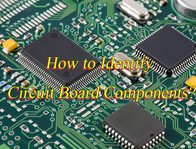
What is a PCB? PCB meaning circuit board, a basic structure that uses copper foil traces instead of wires to connect and support electronic components. It enables various components to communicate with each other and work together, making modern electronic products reliable, efficient and easy to manufacture.

What is a PCB? What does PCB meaning?

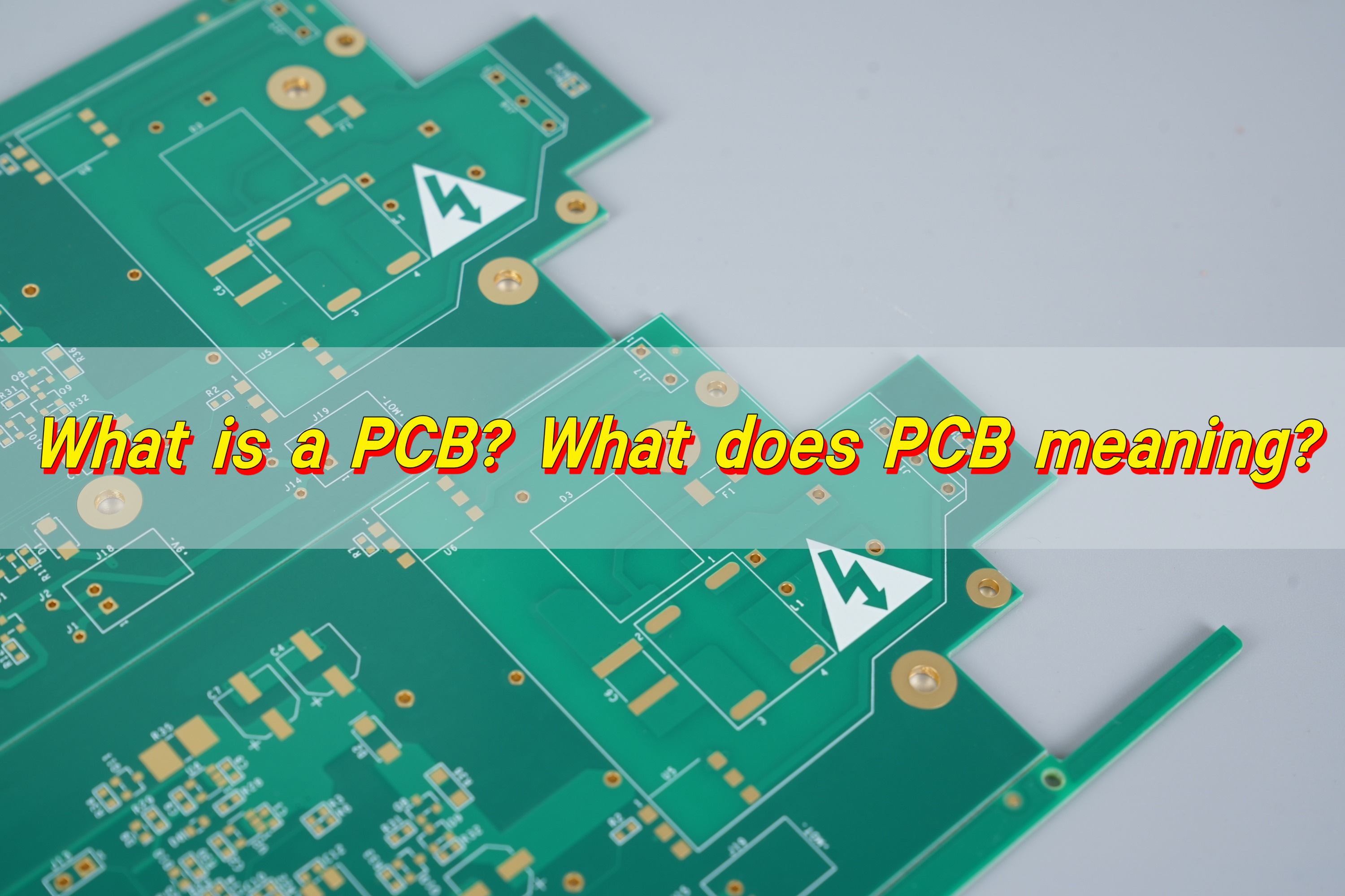
What is a PCB board?

PCB board is the backbone of almost every device you use each day. It holds circuit board components in fixed positions. It directs signals through copper traces. It creates dependable communication between every part of the device.

When you look at a phone, a watch, a smart home tool, a medical meter, or an automotive controller, there is always a PCB board inside doing the heavy work. It delivers smooth performance. It keeps the device compact. It protects circuits from breaking under pressure. It ensures the final product feels solid and reliable.

PCB boards were chosen because they have a simple structure and stable function. Without them, electronics would be messy, bulky, and fragile. Devices would shake apart. Signals would not follow the right direction. And even simple gadgets would become complicated to build.

As a professional manufacturer, Best Technology Co., Ltd. understands the impact of high-quality PCB boards on product success. And that is why a PCB board matters. It is simple, powerful, and essential.

What is a PCB simple definition?

A PCB simplest definition is this: PCB is a board that connects electronic components through printed copper paths.

A PCB supports components and lets electricity travel across the board in a controlled way. That is the core. That is the purpose.

What does PCB stand for?

PCB stands for Printed Circuit Board. The word ā€œprintedā€ reflects the way copper pathways are created on the board. These pathways are not drawn by hand. They are produced through precise manufacturing steps that form thin lines of copper on the surface.

The term ā€œcircuitā€ represents the flow of electricity. It includes every trace, via, component pad, and copper area. The board becomes a complete road map for electric energy.

The word ā€œboardā€ describes the physical shape. It is flat. It is strong. It is usually made from reinforced fiberglass material like FR-4. It supports all circuit board components in one place.

Together, the three words create the term Printed Circuit Board. A PCB is a board that carries circuits created through printed patterns. The meaning of PCB has become universal in the electronics world.

Best Technology produces PCBs for global customers. No matter the product, a PCB provides the structure for electronics to work.

What is the difference between a circuit board and a PCB?

Circuit board is a broader category. It includes any type of board used to connect circuits. That means prototype boards, breadboards, wired boards, and printed boards all belong to this category.

PCB is a specific type of circuit board. It uses printed copper traces instead of wires. Its structure follows professional manufacturing steps. It is cleaner. It is stronger. It is designed for mass production.

So every PCB is a circuit board. But not every circuit board is a PCB.

What is a PCB? What does PCB meaning?

The industry usually uses ā€œPCBā€ when speaking about real products because PCB ensures consistency. It allows automated assembly. It supports mass manufacturing. It keeps signal quality high. Other types of circuit boards work for learning or testing, but they are not built for final production.

How does PCB board work?

PCB board works by transferring electrical signals through copper pathways. These pathways connect each component in a precise pattern. When power enters the system, the path guides electricity to every part that needs it.

When the mapping is clean, the signal stays stable. When the copper lines follow the right width and spacing, the system becomes smooth and safe. And when the entire board is designed well, heat stays under control. Performance becomes more reliable.

PCB board can have one layer, two layers, or multiple layers stacked together. More layers mean more complex functions. Modern devices often use multi-layer designs because they allow compact size and high performance at the same time.

Best Technology builds boards with 2, 4, 6, 8, and even over 20 layers. Each one works by guiding signals with precision. The success of the final device always depends on how well the PCB board works inside it.

What is a PCB layout?

PCB layout is the visual and functional design of a PCB. It shows where each trace goes. It shows where each component stays. It displays the direction of every signal. And it lays out the full structure of the board so manufacturing can begin. Engineers create this layout using professional software.

A layout includes:

  • Component placement
  • Copper routing
  • Power and ground planes
  • Mounting holes
  • Vias
  • Silkscreen text
  • Board outlines

The layout is one of the most important steps in PCB design. A clear layout improves performance. A poor layout can cause noise, interference, or heat issues.

Best Technology Co., Ltd. works closely with clients during layout evaluation to ensure that each PCB can move smoothly into manufacturing without delays.

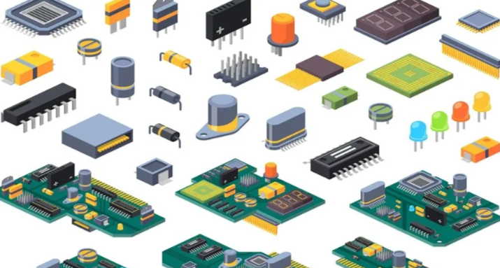
What is a PCB board made of?

PCB board is made of layered materials that work together to create strength, insulation, and electrical conduction. The structure looks simple on the surface, but the layers have important roles.

  • 1. Base Material (Substrate)

The base is usually FR-4, a fiberglass epoxy that provides strength and insulation. Other materials include Rogers high-frequency laminates, polyimide for flexible boards, and aluminum for heat-intensive devices.

  • 2. Copper Layer

This layer carries the signals. It can be 1-oz, 2-oz, or thicker, depending on current needs.

  • 3. Solder Mask

This is the green, blue, red, yellow, or black coating seen on PCBs. It protects copper traces from oxidation and prevents solder bridging.

  • 4. Silkscreen

This is the white print on top. It marks labels, numbers, and component guides.

  • 5. Surface Finish

To ensure solder quality, manufacturers apply finishes like ENIG, HASL, OSP, immersion tin, or immersion silver.

Together, these layers form a strong, reliable platform. Best Technology selects materials based on customer needs. High-frequency devices need special laminates. Automotive boards need heat-resistant substrates. LED boards need aluminum-backed structures for better cooling.

What is a PCB board used for?

A PCB board is used in nearly every electronic product on the market. It supports devices that shape daily life, business, entertainment, health, communication, and transportation.

  • Phones use PCBs to process signals, display screens, and control sensors.
  • Medical tools use PCBs to read data and deliver accurate measurements.
  • Automobiles use PCBs to manage engine control, safety features, lighting, navigation, and audio.
  • Smart home devices use PCBs to connect to the internet and deliver smart functions.
  • Industrial machines rely on PCBs to automate processes and secure stable operation.

PCBs are located inside the product, connecting all components together to ensure the system functions properly. Best Technology supplies PCB boards to companies that build consumer electronics, communication systems, industrial tools, automotive modules, and medical devices.

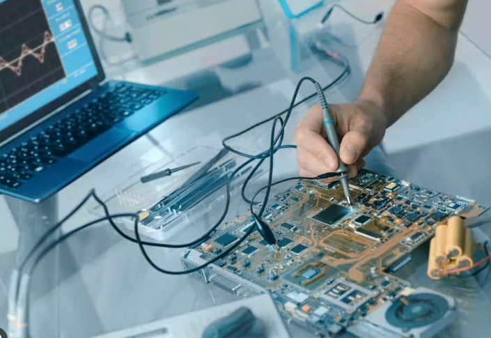
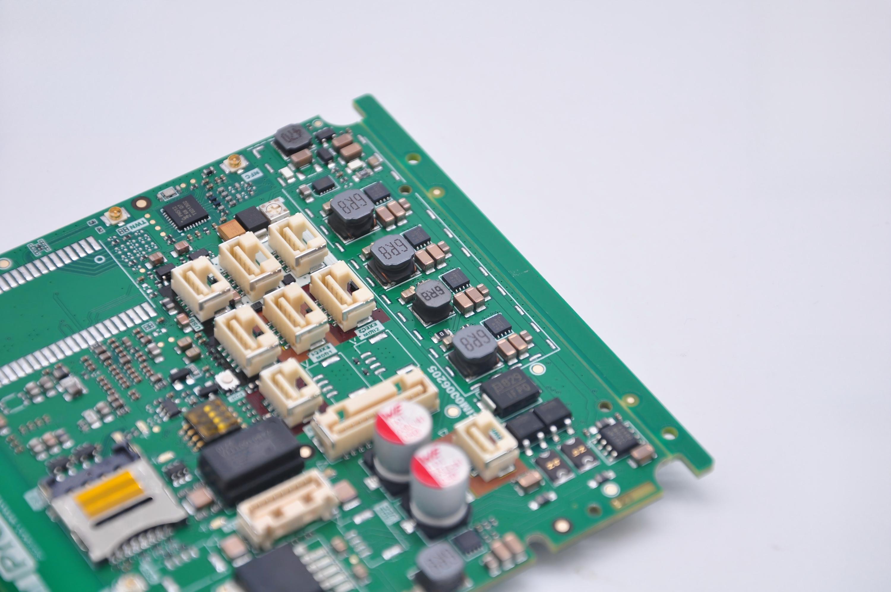
What is a PCB assembly?

PCB assembly, also known as printed circuit board assembly, is the process that mounts components onto the PCB. The PCB only becomes a functional electronic device after assembly.

PCB assembly includes:

  • Solder paste printing
  • Pick-and-place
  • Reflow soldering
  • Wave soldering (for through-hole)
  • AOI inspection
  • X-ray inspection
  • Manual touch-up
  • Final testing

This process turns the board from a simple platform into a working circuit system.

Best Technology Co., Ltd. offers both PCB fabrication and PCB assembly services, making it a one-stop solution for clients who want faster production and better coordination.

Best Technology offers turnkey PCB assembly with fast delivery, stable quality, and strong engineering support. Our experience makes PCBA smoother and more dependable for customers worldwide.

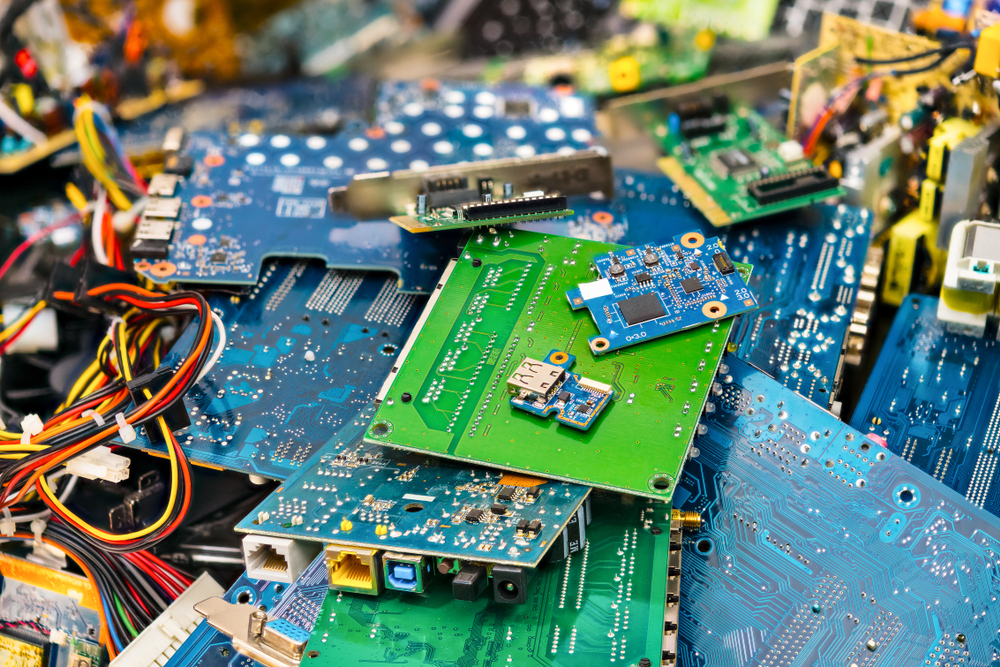
What Is the Difference Between PCBA and PCB?

PCBA and PCB may look similar, but they represent different stages of production.

  • PCB is the bare board. It has copper traces but no components.
  • PCBA is the assembled board. It includes resistors, chips, connectors, sensors, and all other parts required to make the circuit operate.

Both are important. Both support the final product. Both must meet quality standards. But only the PCBA performs the actual function of the device.

What is a PCB? What does PCB meaning?

Best Technology offers both PCB fabrication and full PCBA services. Customers trust the company because one-stop service avoids communication gaps. It creates faster production. It reduces delays. And it keeps the final product consistent.

Conclusion:

PCB is more than a simple board. It is the strength behind modern electronics. From layout to materials, from components to assembly, every step shapes performance. Best Technology Co., Ltd. supports projects with reliable PCB boards and professional printed circuit board assembly.

If you need PCBs, PCBA, or support for your next electronic project, feel free to contact: sales@bestpcbs.com

How to Identify Circuit Board Components​?
Thursday, October 16th, 2025

How to choose circuit board components? Let’s discover its selection guide, component list, Identification and removal methods, test and troubleshoot guide.

Are you worried about these problems?

  • Long lead time for urgent orders? 72-hour rapid prototyping, 30% shorter lead time!
  • High costs due to component shortages? Precise component matching, 15%-25% lower procurement costs!
  • Unstable yield rates? Smart process parameter locking, rework rate comparable to top 3 in the industry!

As a professional PCBA service supplier, Best Technology can provide you service:

  • Fast: Rapid response to small-batch urgent orders, no delays in product launch;
  • Cost-saving: 20 years of component database experience, early shortage warnings, direct cost reduction;
  • Stable: Standardized process parameters, stable yield rates, lower rework rates, more reliable mass production!

Welcome to contact us if you have any request for circuit board components: sales@bestpcbs.com.

How to Choose Circuit Board Components?

Below is a guide to how to choose circuit board components:

1. Prioritize Technical Parameters

  • Define core electrical specifications (voltage/current/frequency) and physical constraints (size/weight), prioritizing critical performance metrics. Example: High-frequency circuits require low-loss dielectric materials (e.g., Rogers RO4350B), while power devices demand thermal resistance assessment.
  • Create a technical specification sheet marking mandatory parameters (e.g., ±5% tolerance) and negotiable items.

2. Validate Environmental Adaptability

  • Test component reliability for target market environments: Industrial applications require -40°C~125°C operating ranges, consumer electronics need 85°C/85%RH humidity resistance, and automotive components must meet AEC-Q200 standards.
  • Action: Request third-party test reports (e.g., UL certification, SGS salt spray testing) with emphasis on temperature cycling curves and ESD protection levels.

3. Assess Supply Chain Reliability

  • Select ISO9001/IATF16949-certified suppliers, favoring multinational brands with local technical support (e.g., TDK, Murata). For critical components (e.g., processors), secure at least a 2-year supply guarantee agreement.
  • Action: Evaluate suppliers using a Scorecard for on-time delivery (≄95%), yield rate (≄99.2%), and quality system maturity.

4. Conduct Compatibility Verification

  • Verify electrical compatibility through experiments: Use network analyzers for S-parameter testing to confirm impedance matching, and thermal imagers to monitor power module temperature distribution. For digital circuits, validate timing margins (Setup/Hold Time).
  • Action: Build prototype platforms for 500+ hour continuous aging tests, documenting failure modes and analysis reports.

5. Balance Cost and Maintainability

  • Optimize costs via value engineering: Use commercial-grade components (e.g., 0402 capacitors) in non-critical paths, while critical modules adopt automotive-grade devices. Design modular plug-and-play structures to reduce maintenance costs.
  • Action: Prepare BOM cost comparison tables detailing unit costs, MOQ requirements, lead times, and total cost of ownership (TCO).
How to Choose Circuit Board Components?

Common Circuit Board Component List

Resistor

  • Function: Current limiting, voltage division, impedance matching.
  • Type: Carbon film resistor, metal film resistor, SMD resistor (0603/0805 package), 0Ī© resistor (jumper), variable resistor (potentiometer).
  • Parameters: Resistance (Ī©), power rating (W), tolerance (±1%~±5%), temperature coefficient (ppm/°C).
  • Application: Power management, signal conditioning, EMI suppression.

Capacitor

  • Function: Filtering, energy storage, coupling, decoupling.
  • Type: Polarized electrolyytic capacitor, ceramic capacitor (X7R/X5R/NPO), film capacitor, tantalum capacitor, supercapacitor.
  • Parameters: Capacitance (pF~μF), voltage rating (V), ESR (mĪ©), leakage current (μA).
  • Application: Power bypass, signal coupling, timing circuits.

Inductor

  • Function: Energy storage, filtering, anti-interference.
  • Type: Coil inductor, SMD inductor, magnetic bead, common-mode choke.
  • Parameters: Inductance (μH~mH), Q value, current rating (A), DC resistance (mĪ©).
  • Application: Switching power supply filtering, EMI suppression, LC resonance.

Diode

  • Function: Rectification, voltage regulation, light emission, protection.
  • Type: Rectifier diode (1N4007), Schottky diode (low Vf), Zener diode, LED, TVS (transient suppression).
  • Parameters: Forward voltage (V), reverse breakdown voltage (V), maximum current (A), recovery time (ns).
  • Application: Power rectification, signal protection, status indication.

Transistor/MOSFET

  • Function: Amplification, switching control.
  • Type: NPN/PNP transistor, N/P-channel MOSFET, IGBT, JFET.
  • Parameters: Vceo (V), Ic (A), hFE, Vgs(th) (V), RDS(on) (Ī©).
  • Application: Signal amplification, switching power supplies, motor drives.

Integrated Circuit (IC)

  • Function: Signal processing, control, storage.
  • Type: Microprocessor (STM32), power management chip, op-amp, logic gate, memory (EEPROM/Flash), ASIC.
  • Parameters: Operating voltage (V), temperature range (ā„ƒ), power consumption (mW), package (QFP/BGA).
  • Application: System control, data processing, power management.

Connector

  • Function: Board-to-board/cable connection.
  • Type: Pin header/socket, USB interface, RJ45 port, SIM card holder, FPC connector.
  • Parameters: Pin count, current rating (A), signal rate (Gbps), waterproof rating (IPXX).
  • Application: Modular design, high-speed data transmission, external device connection.

Switch/Button

  • Function: Manual circuit on/off control.
  • Type: Toggle switch, push-button switch, tactile switch, rotary potentiometer, DIP switch.
  • Parameters: Rated voltage/current, mechanical life (cycles), contact resistance (mĪ©).
  • Application: User input, mode switching, parameter adjustment.

Sensor

  • Function: Environmental parameter detection.
  • Type: Temperature sensor (DS18B20), photoresistor, accelerometer, pressure sensor, humidity sensor.
  • Parameters: Measurement range, accuracy, response time, output type (analog/digital).
  • Application: Environmental monitoring, industrial control, medical diagnostics.

Protection Component

  • Function: Over-current/over-voltage protection.
  • Type: Fuse, PTC thermistor, TVS diode, varistor.
  • Parameters: Current rating (A), breakdown voltage (V), response time (ns).
  • Application: Circuit safety protection, lightning protection, ESD protection.

Crystal Oscillator & Resonator

  • Function: Clock signal generation.
  • Type: Crystal oscillator (32.768kHz), ceramic resonator, crystal module.
  • Parameters: Frequency accuracy (ppm), load capacitance (pF), operating temperature range (ā„ƒ).
  • Application: Microprocessor clock, timing circuits, communication modules.

RF & Antenna Components

  • Function: Wireless signal transmission/reception.
  • Type: PCB antenna, SMA RF connector, filter, low-noise amplifier (LNA).
  • Parameters: Frequency range (MHz~GHz), insertion loss (dB), VSWR.
  • Application: Wireless communication (WiFi/Bluetooth), radar, navigation.

Battery & Power Interface

  • Function: Power supply & energy storage.
  • Type: Lithium battery, coin cell, DC power jack, charging management chip.
  • Parameters: Battery capacity (mAh), charging current (mA), output voltage (V).
  • Application: Portable device power supply, power adaptation, energy storage.

Marking & Test Points

  • Function: Function marking & test interface.
  • Type: Silkscreen marking, test pad, via, debug interface (JTAG/UART).
  • Application: Production identification, fault troubleshooting, function debugging.

How to Identify Circuit Board Components​?

Circuit Board Components Identification Methods:

1. Identify Passive Components (Resistors/Capacitors/Inductors)

  • Resistors: Determine resistance via color bands or numeric codes. For 4-band resistors, first two bands represent significant figures, third band multiplier, fourth band tolerance (e.g., “brown-black-red-gold” = 1kĪ© ±5%). For 5-band resistors, first three bands are significant figures, fourth band multiplier, fifth band tolerance. SMD resistors use numeric codes (e.g., “472” = 47Ɨ10²Ω = 4.7kĪ©).
  • Capacitors: Polarized electrolyytic capacitors feature polarity markings (“+” or notch) and value labels (e.g., “10μF/16V”). Ceramic/SMD capacitors use numeric codes (e.g., “104” = 10Ɨ10⁓pF = 0.1μF). Unit conversions: 1F = 10⁶μF = 10¹²pF.
  • Inductors: Coil structures are visually identifiable, labeled “L” + number (e.g., “L1”). Color-coded inductors follow resistor-like decoding (e.g., brown-black-gold = 1μH ±5%).

2. Identify Semiconductor Devices (Diodes/Transistors)

  • Diodes: Marked “D” + number; cathode identified via band or shorter lead. LEDs have anode (longer lead) and cathode. Use multimeter diode mode: forward voltage drop ā‰ˆ0.7V (silicon) or 0.3V (germanium).
  • Transistors: Labeled “Q” + number; NPN/PNP types determined via pinout or model number (e.g., 9013 = NPN, 9012 = PNP). Pin sequence: base (B), collector (C), emitter (E). Verify via datasheet.

3. Identify Integrated Circuits (ICs)

  • Marking: Surface-printed model (e.g., “ATmega328P”) or “U1” reference. Pin counts range from DIP (dual in-line package) to QFP (quad flat package). SMD ICs labeled “IC” + number; confirm function via datasheet.
  • Packaging: Through-hole (DIP) allows visual pin inspection; SMD requires silkscreen layer numbering. Multi-layer boards utilize vias for interlayer connections.

4. Leverage Tools for Identification

  • Multimeter: Resistance mode for resistors, diode mode for diodes, capacitance mode for capacitors (discharge before testing).
  • Magnification Tools: Magnifying glass/microscope for inspecting micro-components (e.g., 0805 resistors) or solder joint quality.
  • Schematic Comparison: Cross-reference schematic symbols (e.g., “R” = resistor, “C” = capacitor) with physical silkscreen labels.

5. Special Components & Safety Notes

  • Polarized Components: Electrolyytic capacitors, diodes, lithium batteries require correct polarity orientation; reverse connection risks damage.
  • Package Recognition: TO-220 packages may house transistors, MOSFETs, or voltage regulators; SOP packages common for ICs.
  • Safe Practices: Operate with power disconnected; prevent electrostatic discharge (ESD) damage. Soldering temperature controlled below 350°C.
How to Identify Circuit Board Components​?

How to Remove Circuit Board Components​?

1. Tools and Materials Preparation

Advanced Tool Selection

  • Use a temperature-adjustable soldering iron (30-40W, 300-400°C) with interchangeable tips: chisel, knife, and conical types. A hot air gun with dual-control (airflow 20-30L/min, temperature 300-380°C) and anti-static nozzle is recommended.

Material Specifications

  • Solder wire: lead-free Sn96.5Ag3Cu0.5 alloy, 0.5-1.0mm diameter. Flux: acidic (cleaning-type) or neutral (no-clean) for dense component areas. Solder wick: braided copper mesh matching pad dimensions.

2. Pre-Operation Preparation

  • Component Marking System: Label component parameters (e.g., capacitor polarity “+”, IC notch direction) using oil-based markers. For multi-pin ICs, sketch pin layouts and mark critical pins (VCC, GND). Document with HDR-mode photos for weld detail enhancement.
  • Safety Environment Setup: Workbench with ESD-safe rubber mat and grounded wrist strap (resistance <10⁶Ω). Ventilation system maintains ≄12 air changes/hour to prevent flux fume accumulation.

3. Component-Specific Removal Techniques

  • Small Components (0402/0603 SMDs): Employ “drag-soldering”: angle soldering iron at 45°, heat for 2-3 seconds, then slide along pin to melt solder evenly. Extract vertically with non-magnetic tweezers to avoid pad lifting.
  • Multi-Pin ICs (QFP/LQFP Packages): Apply “spiral heating”: start at IC center, heat outward in clockwise direction at 45° angle, 10-15mm distance. Alternate 3-second heating/1-second pause until solder liquefies. Use vacuum tweezers for extraction.

Large Components (Axial Electrolytic Capacitors)

  • Implement “dual-zone isolation”: place solder wick on both pads, heat simultaneously with two irons. Rotate leads 90° slowly after solder melt to distribute residue onto wick. Pre-discharge high-capacity capacitors via 100Ī© resistor.

4. Advanced Scenario Handling

  • BGA Chip Decapsulation: Utilize BGA rework station with three-stage heating: 150°C/30s preheat, 280°C/40s main heat, 50°C/60s cooldown. Post-removal X-ray inspection verifies solder ball integrity.
  • Dense FPC Connectors: Apply “low-temperature stripping”: coat pins with 138°C melting solder paste, heat at 180°C with hot air gun. Separate gently using plastic pry tools to avoid trace damage.

5. Safety and Maintenance Protocols

  • Pad Integrity Verification: Inspect pads under 50x magnifier for lifting, cracks, or delamination. Minor damage repaired with conductive silver paste; severe cases require copper trace reconstruction.
  • Tool Maintenance Standards: Clean soldering iron tips daily with brass brush, then tin for oxidation protection. Monthly ultrasonic cleaning of hot air gun filters maintains airflow efficiency.
  • Waste Management: Segregate lead-free and leaded solder waste. Lead-containing residue requires certified disposal. Used wick/swabs stored in metal containment bins separate from general trash.

How to Solder Circuit Board Components​?

1. Tools and Materials Preparation

  • Soldering iron (30-40W), rosin-core solder wire (0.5-1mm diameter), solder sucker, non-magnetic tweezers, ESD wrist strap, magnifier/desk lamp, cleaning sponge, flux (optional).
  • Inspect circuit board pads for oxidation; gently polish with sandpaper until shiny. Check component leads for oxidation or dirt, scrape lightly with a blade if necessary.

2. Component Positioning and Fixing

  • Insert components into corresponding pad holes per circuit diagram. Through-hole components (e.g., resistors, capacitors) must be vertical; SMD components are lightly pressed onto pads with tweezers.
  • Large components (e.g., sockets, large capacitors) can be temporarily fixed with a small amount of solder on 1-2 leads to prevent sliding. SMD components may use dedicated fixtures.

3. Soldering Operation Steps

  • Preheat soldering iron: Clean tip with sponge until silver-white, apply a small solder layer for oxidation prevention. Set temperature to 300-350ā„ƒ (general components) or 350-400ā„ƒ (large pads/grounding).
  • Heat pad and lead: Simultaneously contact both pad and lead with iron tip for 2-3 seconds for even heating.
  • Feed solder and shape: Feed solder wire on the opposite side of the iron tip. Once solder melts and coats both pad and lead evenly, remove solder wire first, then slowly lift the iron to avoid stringing.
  • Cooling inspection: After cooling, check for smooth conical solder joints free of cracks, burrs, or cold solder (use magnifier).

4. Solder Joint Quality and Troubleshooting

  • Cold solder detection: Gently pull the component lead; if the joint detaches, re-solder. Verify conductivity with multimeter.
  • Bridge handling: For shorted adjacent joints, use solder sucker to remove excess solder or drag melted solder away with iron.
  • Cold solder repair: Reheat dull, matte solder joints until molten, then allow natural cooling.

5. Safety and Maintenance

  • Wear ESD wrist strap to prevent static damage to sensitive components. Keep work area dry and away from flammable materials.
  • Turn off soldering iron when not in use to avoid overheating. Regularly clean iron tip oxide and maintain sharpness.
  • Post-soldering: Clean flux residue with alcohol swabs to prevent long-term pad corrosion.

6. Special Component Soldering Techniques

  • SMD components: Apply small solder to one pad, fix component with tweezers, then drag-solder the opposite side. Alternatively, use hot air gun for even heating.
  • Sensitive components (e.g., transistors, ICs): Use “tack soldering”—brief contact with lead to minimize thermal damage risk.

7. Soldering Precautions

  • Limit single-point heating to ≤5 seconds to prevent pad lifting, component internal damage, or PCB substrate charring.
  • For large pads or ground planes, adopt “segmented heating”: 2-3 short heating cycles with solder feeding to ensure uniform heat distribution and reduce thermal stress concentration.

How to Test Circuit Board Components with Multimeter​?

1. Resistor Testing

  • Power Down & Discharge: Ensure the circuit is fully powered off. For capacitors, discharge by shorting their leads.
  • Range Selection: Use the multimeter’s resistance range (e.g., RX10k, RX1k). Start from the highest range and adjust downward until the reading stabilizes near the resistor’s rated value to avoid meter damage.
  • Connection & Reading: Touch probes to both resistor terminals (no polarity). Compare measured resistance to the labeled value. A deviation exceeding ±20%, or readings of “0”/”āˆž”, indicates failure.
  • Low-Resistance Handling: For resistors below 10Ī©, use a 4-wire (Kelvin) method to eliminate lead resistance or bypass PCB traces during measurement.

2. Capacitor Testing

  • Discharge First: Discharge large capacitors via a resistor; short small capacitors’ leads.
  • Direct Capacitance Measurement: Use the multimeter’s capacitance range. Select an appropriate scale (e.g., 200μF range for a 10μF capacitor). For polarized capacitors (e.g., electrolytic), connect the red probe to the positive terminal.
  • Resistance/Diode Mode Verification:
  • Resistance Mode: For large capacitors, use a low range (<10kĪ©); observe charging (resistance rises from 0 to āˆž). For small capacitors, use a higher range for clearer changes.
  • Diode Mode: A ~2.7V drop between probes is applied. Monitor charging until the resistance stabilizes.
  • Fault Detection: A functional capacitor shows near-infinite resistance after charging. Short circuits or leakage cause abnormally low resistance.

3. Diode Testing

  • Polarity Check: Use diode or resistance mode (RƗ1k). Forward-biased (red probe to anode) shows low resistance (~0.6V for silicon, ~0.2V for germanium). Reverse-biased shows high resistance.
  • Fault Identification: Bidirectional conduction or blockage indicates failure. Excessive forward resistance or reverse leakage signals degradation.
  • High-Voltage Diodes: Use RƗ10k range. Forward resistance should exceed 10kĪ©; reverse should read infinite. Reverse breakdown requires specialized tools.

4. Transistor Testing

  • Pin & Type Identification:
  • Base Detection: In RƗ1k mode, touch one probe to a terminal; if the other two terminals show conduction, it’s the base. Red probe to base for PNP, black for NPN.
  • Collector/Emitter: Measure resistance (e.g., for NPN: black to collector, red to emitter shows low resistance).
  • Performance Verification:
  • Junction Resistance: Emitter/collector junctions show forward conduction (~1kĪ©) and reverse blockage (infinite).
  • Current Gain (hFE): Use the dedicated hFE socket or measure collector current variation via base resistor.
  • Leakage Current: Reverse collector-emitter resistance should be high (e.g., >100kĪ© for silicon).

5. Critical Safety & Best Practices

  • Safety First: Always power off circuits. Use insulated tools and one-hand operation for high-voltage measurements. After testing, set the multimeter to the highest AC voltage range.
  • Range Management: Start with the highest range for unknown values; reduce incrementally. Avoid body interference when measuring high resistance.
  • Polarity Accuracy: Digital meters: red probe = positive; analog meters: opposite. Correct polarity is crucial for polarized components (e.g., electrolytic capacitors, diodes).
  • Avoid Measurement Errors: Never use resistance mode on live circuits. Do not measure voltage with current mode. Avoid detecting microvolt-level signals with standard multimeters.
How to Test Circuit Board Components with Multimeter​?

How to Troubleshoot Circuit Board Components?

1. Visual Pre-Inspection

  • Use magnifier/microscope to inspect solder joints: check for cold solder joints, fractures, or solder bridges (shorts between adjacent pads). Focus on BGA chip edges and SMD component pins.
  • Examine component physical state: capacitors for bulging/leakage; resistors for burn marks; diodes/transistors for oxidized/broken leads; IC pins for bending/deformation.
  • Inspect PCB copper layers: signs of burn marks, corrosion breaks, mechanical scratches, or debris (e.g., metal fragments causing shorts).

2. Power & Ground Testing

  • Static voltage measurement: Measure voltage rails (e.g., 5V, 3.3V, 12V) against ground after power-up. Deviations >±5% indicate anomalies (e.g., 4.2V on 5V rail suggests overcurrent/load or faulty regulator).
  • Short-circuit localization: With power off, use multimeter continuity mode to measure rail-to-ground resistance. Resistance <20Ī© requires thermal imaging or segmented power-down to locate shorts.
  • Ground continuity check: Verify all ground pads to main ground plane resistance <1Ī© to eliminate solder joint failures or oxidation.

3. Signal Path Tracing

  • Critical signal measurement: Use oscilloscope to check clock/data/control signal amplitude, frequency, and rise time. Insufficient clock amplitude (<1.5V) may indicate driver weakness or overload.
  • Signal integrity analysis: Check high-speed signals for overshoot/ringing/crosstalk. Improve with termination resistors or added filtering capacitors.
  • Open-circuit detection: Use jumper wires to bridge suspected breaks (e.g., fine wire across fractured traces) to confirm fault location via functional recovery.

4. Component Function Verification

  • Resistor/capacitor testing: Measure resistance/capacitance offline with multimeter/LCR meter. Discharge capacitors first; replace electrolyytics with >±20% deviation or high ESR.
  • Diode/transistor testing: Use diode mode to check forward (0.5-0.7V Si) and reverse (infinite) voltage drops. Test transistor junction resistances and hFE gain.
  • IC functional testing: For pins-driven ICs, force inputs to observe outputs (e.g., logic gate input HIGH should yield output LOW).

5. Substitution & Comparative Validation

  • Suspect component replacement: Swap with known-good components (e.g., caps/resistors/transistors) to confirm failure via fault resolution.
  • Comparative analysis: Contrast waveforms/voltages/frequencies against working boards (e.g., 50kHz vs. 100kHz clock indicates source fault).
  • Minimal system test: Remove peripheral modules (sensors/interfaces) incrementally to isolate core circuit functionality.

6. Environmental & Auxiliary Checks

  • Thermal scanning: Use IR thermography to detect overheating (>20% above design temp) indicating overcurrent or poor cooling.
  • Vibration testing: Tap components/connectors to diagnose intermittent faults from poor contacts or micro-fractures.
  • ESD protection: Discharge static via grounded metal before handling; use ESD-safe tools to prevent sensitive component damage.

7. Firmware & Configuration Verification

  • Firmware version check: Read MCU/memory/FPGA firmware via programmer; compare with official releases. Mismatches require reflashing.
  • Register configuration audit: For programmable components (e.g., op-amps/power ICs), verify registers (gain/frequency/enable) via I?C/SPI. Misconfigurations cause distortion.
  • Software logic validation: Use logic analyzer to capture control signals (CS/INT/WR); analyze for software delays/race conditions/protocol errors (e.g., SPI timing errors from delay settings).
  • Boundary scan testing: For complex digital circuits (BGA), use JTAG to detect pin opens/shorts/internal logic faults in hidden solder joints.
How to Troubleshoot Circuit Board Components?

Where Can I Buy Circuit Board Components?

Offline Professional Electronic Markets – Intuitive Experience, Instant Transactions

  • Recommended Scenarios: Suitable for users needing on-site quality inspection and immediate transactions. Examples include Hong Kong Mong Kok Electronic Market (Asia’s leading electronics hub with direct supplier access) and New York City’s Canal Street Electronics District (renowned for component variety and real-time testing).
  • Advantages: Direct parameter testing (e.g., resistance/capacitance verification) to avoid online description mismatches; flexible pricing for small-batch purchases.
  • Notes: Research global market price benchmarks in advance; prioritize authorized brand counters to minimize counterfeit risks.

Global E-Commerce Platforms – Transparent Pricing, User Reviews

  • Recommended Platforms: Amazon Business, eBay, AliExpress Global (use precise search terms like “0805 SMD resistor 100 ohm Kyocera”).
  • Advantages: Multi-store price comparison with transparent pricing; platforms offer guarantees like “A-to-Z Protection” (Amazon) or “Authenticity Guarantee” (eBay).
  • Notes: Optimize for “Top-Rated Sellers” or “Brand Flagship Stores”; verify parameters with a multimeter upon delivery and retain transaction records.

International Professional Component Platforms – Authenticity & Technical Resources

  • Recommended Platforms: Digi-Key (US-based, 15M+ SKUs, 72-hour global delivery), Mouser Electronics (Texas-based, 2900+ authorized manufacturers), Arrow Electronics (Colorado-based, IoT/5G specialists), RS Components (UK-based, European coverage), TME (Poland-based, Central Europe leader), Farnell (UK-based, engineering-focused).
  • Advantages: Full technical datasheets, real-time inventory updates; small-batch support with free shipping on select platforms; specialized support for R&D teams.
  • Notes: Account for customs duties and extended logistics times for international shipments; prioritize “in-stock” filters to avoid future delays.

Manufacturer Direct/Authorized Distributors – Pricing & Customization

  • Recommended Channels: Direct contact with global manufacturers (TI, ADI, STMicroelectronics) or authorized distributors (Avnet, Future Electronics, Digi-Key as distributor).
  • Advantages: Volume discounts for bulk purchases; support for custom parameters (e.g., high-temperature capacitors); access to official technical support and certification documents.
  • Notes: Verify distributor authorization via official websites (e.g., check Arrow’s global partner list); small-batch purchases may incur higher unit costs—balance with project needs.

International Second-Hand/Salvaged Component Markets – Cost-Effective Solutions

  • Recommended Channels: eBay (global marketplace with verified sellers), Swappa (specialized electronics marketplace with payment protection), Gazelle (certified refurbished devices), Amazon Renewed (premium refurbished goods with warranty).
  • Advantages: Low-cost options for non-critical applications (e.g., prototyping); some salvaged components offer stable performance with verified testing reports.
  • Notes: Explicitly confirm “used/refurbished” status; request high-resolution photos/testing videos from sellers; prioritize sellers with high feedback scores and global shipping capabilities.

Welcome to contact us if you have any request for circuit board components: sales@bestpcbs.com.