

Seeking for a competitive 4 layer PCB board solution? Explore its definition, stack-up structure, thickness, design guidelines, manufacturer selection tips.
EBest Circuit (Best Technology) specialize in delivering high-quality 4 layer PCBs with unmatched speed and customization: our streamlined process ensures 48-hour rapid prototyping for urgent orders, allowing you to meet tight deadlines without compromising on quality. Whether you need a single prototype or small batches, we support no minimum order quantity—start with 1 piece and scale as needed. Our service includes free DFM (Design for Manufacturing) analysis, where our experienced engineers provide detailed feedback to optimize your design for production, saving you time and costs upfront. Plus, enjoy one-on-one online engineering support throughout the process, ensuring clear communication and quick adjustments. As an ISO-certified manufacturer, we adhere to strict quality standards, conducting 70+ checks including AOI, X-ray, and impedance testing, while offering materials like FR4, Rogers, and thick copper (up to 30 oz) to meet diverse technical requirements. Trusted by global clients across industries, we deliver export-ready PCBs with transparent pricing, no hidden fees, and efficient logistics. Ready to bring your 4 layer PCB board project to life? Contact us today for a personalized quote and experience how our speed, flexibility, and technical expertise can drive your success: sales@bestpcbs.com.
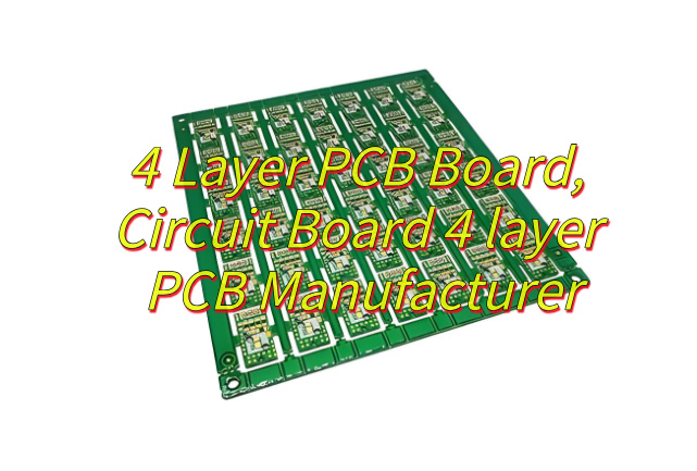
What Is a 4 Layer PCB Board?
A 4 layer PCB board is a printed circuit board comprising four conductive layers interleaved with insulating materials. Unlike 2-layer PCBs, which only have top and bottom signal layers, 4-layer boards integrate two additional inner layers—typically a power plane and a ground plane. This configuration enables efficient power distribution, minimized electromagnetic interference (EMI), and improved signal integrity. The layers are bonded together using prepregs (pre-impregnated resin sheets) and cores, creating a rigid structure suitable for high-density applications. Common uses include automotive electronics, industrial control systems, and consumer devices where compact size and robust performance are critical.
What Is Stack-up of 4-Layer PCB?
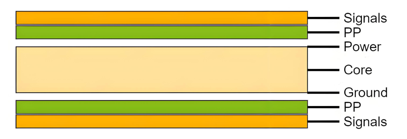
Here are the three common stack-up of 4- layer PCB configurations:
For Consumer Electronics & Moderate-speed Applications: Signal-Power-Ground-Signal
- Top layer: Signal routing and component placement.
- Inner layer 1: Power plane (VCC) for stable voltage distribution.
- Inner layer 2: Ground plane (GND) to minimize noise and provide a low-impedance return path.
- Bottom layer: Signal routing and additional components.
For High-speed Applications: Signal-Ground-Power-Signal
- Top layer: Signal routing.
- Inner layer 1: Ground plane (GND) for electromagnetic shielding.
- Inner layer 2: Power plane (VCC) for efficient power delivery.
- Bottom layer: Signal routing.
For Space-Constrained Designs Requiring Extra Routing Layers: Signal-Signal-Power-Ground
- Top layer: Signal routing.
- Inner layer 1: Signal routing (for additional traces).
- Inner layer 2: Power plane (VCC).
- Bottom layer: Ground plane (GND).
What Is Thickness of 4 Layer PCB Board?
The thickness of a 4 layer PCB board depends on material selection, layer count, and application requirements. Here’s a detailed breakdown:
Standard Thickness Range:
- 0.4 mm to 1.6 mm (0.016″ to 0.063″) for most consumer and industrial applications .
- Thicker boards (up to 2.36 mm/0.093″) are used in military or high-power environments requiring enhanced mechanical stability .
Material Contributions:
- Copper foil thickness: 1–3 oz (ounces per square foot) is typical; higher weights (e.g., 30 oz) support high-current applications .
- Dielectric layers: FR4 prepreg thickness ranges from 0.002″ to 0.059″, affecting impedance control and layer spacing.
Design Considerations:
- Aspect ratio (board thickness to hole diameter) should be ≤1:25 for optimal drillability and plating quality .
- Symmetrical stackups (e.g., balanced layer distribution) reduce warping during thermal cycling .
4 Layer PCB Design Guidelines
Below are guidelines of 4 layer PCB design:
1. Layer Stack-up Configuration
Standard Stack-up:
- Layer 1 (Top): Component placement and critical signal routing.
- Layer 2 (Internal 1): Ground plane for reference and noise suppression.
- Layer 3 (Internal 2): Power plane for voltage distribution.
- Layer 4 (Bottom): Secondary signal routing and component placement.
Alternative Stack-up:
- For mixed-signal designs: Separate analog and digital ground planes connected at a single point.
- For high-speed designs: Use a stripline configuration with symmetric ground-signal-ground-power layers.
2. Signal Integrity Management
Controlled Impedance:
- Define trace width/spacing based on dielectric thickness and copper weight (e.g., 50Ω for single-ended traces).
- Use microstrip or strip line configurations for high-speed signals (>1 GHz).
Crosstalk Mitigation:
- Maintain a 3W spacing rule between parallel traces (W = trace width).
- Route sensitive analog lines orthogonally to digital signals.
Differential Pairs:
- Route differential pairs with matched lengths (±0.1 mm tolerance).
- Maintain 2W spacing between pairs to reduce coupling.
3. Power Distribution Network (PDN) Design
Power Planes:
- Use a solid power plane for core voltages (e.g., 3.3V, 5V).
- Split power planes for multiple voltage domains with 0.5 mm isolation gaps.
Decoupling Capacitors:
- Place 0.1 μF ceramic capacitors within 3 mm of IC power pins.
- Add bulk capacitors (10–100 μF) at board-level power entry points.
Via Stitching:
- Stitch power/ground planes with vias every 10–15 mm to reduce inductance.
4. Grounding Strategy
- Single-Point Grounding: Connect analog and digital grounds at one point for mixed-signal circuits.
- Guard Rings: Surround sensitive analog components with grounded traces.
- Thermal Vias: Place vias under high-power components to dissipate heat to internal planes.
5. Component Placement
- Critical Components: Position high-speed ICs (e.g., microcontrollers, FPGAs) near power/ground planes.
- Decoupling Capacitors: Place capacitors in parallel with minimal loop area.
- Connectors: Align connectors with internal signal layers to reduce stub lengths.
6. Routing Priorities
- High-Speed Signals: Route first on the top layer with adjacent ground reference.
- Low-Speed Signals: Route on the bottom layer or internal signal layers.
- Avoid 90° Bends: Use 45° angles or filleted corners to reduce impedance discontinuities.
7. Material Selection
- Dielectric: Choose FR-4 for cost-sensitive designs; use high-frequency laminates (e.g., Rogers 4350B) for >5 GHz applications.
- Copper Weight: Use 1 oz (35 μm) for external layers and 0.5 oz (17.5 μm) for internal layers.
- Surface Finish: Select ENIG for fine-pitch components; use HASL for cost optimization.
8. Manufacturability Considerations
- Minimum Trace/Space: Maintain 6 mil (0.15 mm) for standard fabrication.
- Drill Sizes: Use 0.2 mm vias for cost efficiency; 0.1 mm microvias for HDI designs.
- Panelization: Design boards to fit standard panel sizes (e.g., 500 mm × 600 mm) for efficient production.
9. Thermal Management
- Copper Pours: Add 50% fill-ratio copper pours under high-power components.
- Heat Sinks: Include mounting pads for thermal interface materials (TIMs).
- Metal-Core PCBs: Use aluminum-backed boards for LED lighting or motor drivers.
10. Design for Test (DFT)
- Test Points: Include via-based test points for in-circuit testing (ICT).
- Fiducial Markers: Add 0.5 mm diameter fiducials for automated assembly alignment.
- Boundary Scan: Implement JTAG headers for complex digital circuits.
11. Documentation and Validation
- Design Rules Check (DRC): Run DRC for impedance, clearance, and via constraints.
- Signal Integrity Simulation: Use tools like HyperLynx for pre-layout analysis.
- Gerber Files: Generate extended Gerber (RS-274X) files with layer stack-up documentation.
How to Select A Reliable 4 Layer PCB Board Manufacturer?
Selecting a reliable 4 layer PCB manufacturer requires evaluating their ability to address production :
- Technical Expertise: Experience in multi-layer PCB design, HDI, and high-frequency applications. EBest Circuit (Best Technology)’s 20+ engineers provide SI/PI analysis and DFM checks to optimize manufacturability .
- Certifications: ISO 9001, IATF 16949, or AS9100D certifications for automotive/aerospace compliance. EBest Circuit (Best Technology)’s facilities adhere to strict quality standards .
- Prototyping Capabilities: Rapid turnaround (24–72 hours) for proof-of-concept testing. EBest Circuit (Best Technology) offers 2-layer boards in 24 hours, 4-layer in 48 hours, and 6–8-layer in 72 hours .
- Quality Control: AOI, X-ray, and functional testing to ensure zero defects. EBest Circuit (Best Technology)’s 70+ quality checks include automated optical inspection and impedance testing .
- Transparent Communication: Real-time WIP updates and dedicated project managers to address design adjustments promptly .
- Material Options: Availability of FR4, Rogers, and aluminum-core materials. EBest Circuit (Best Technology) supports metal-core PCBs for high-power applications with thermal conductivity up to 200 W/m·K .
How to Maintain Signal Integrity of Circuit Board 4 layer PCB?
Signal integrity is paramount in 4 layer PCB board design, especially for high-speed interfaces. Implement these strategies:
Crosstalk Mitigation
- Route high-speed signals perpendicular to adjacent layers. Maintain trace spacing of at least 3x the trace width.
- Use ground guards around sensitive signals (e.g., clock lines) to shield against EMI.
Differential Pair Routing
- Match trace lengths for differential pairs (e.g., USB, HDMI) within ±10% to reduce skew. EBest Circuit (Best Technology)’s design tools ensure precise length matching.
- Control differential impedance (e.g., 100Ω for Ethernet) through careful trace width and spacing.
Ground Plane Continuity
- Avoid gaps in ground planes. Use stitching vias every 0.25″ to connect fragmented ground areas .
- Separate analog and digital ground planes and connect them at a single point to minimize noise coupling.
Termination Techniques
- Add series resistors (22–50Ω) to high-speed signals to reduce reflections. For LVDS, use parallel termination at the receiver.
EMI/EMC Control
- Optimize ground plane continuity and avoid split planes to reduce radiation noise.
Signal Return Paths
- Ensure each signal has a low-impedance return path by placing ground planes adjacent to signal layers.
How to Reduce Production Cost of Circuit Board 4 layer PCB?
While 4 layer PCB boards offer superior performance, their cost can be optimized through strategic design and manufacturing choices:
Material Selection
- Use FR4 for most applications; reserve high-cost materials like Rogers for RF or high-frequency needs .
- Standardize on common copper weights (1–2 oz) to leverage economies of scale .
Layer Stack-up Simplification
- Avoid unnecessary layers. A 4-layer board can often replace a 6-layer design with careful routing .
- Consolidate power and ground planes where possible to reduce layer count.
Design for Manufacturability (DFM)
- Minimize blind/buried vias, which increase fabrication complexity. Use through-hole vias for cost-effective production.
- Choose standard drill sizes (≥0.012″) to reduce tooling costs.
Volume Negotiation
- Partner with manufacturers offering tiered pricing for large orders. EBest Circuit (Best Technology) provides competitive rates for bulk production.
Prototyping Efficiency
- Use free DFM analysis to identify and correct design flaws early, avoiding costly reworks.
Via Optimization
- Reduce via count by optimizing routing paths.
Panelization
- Combine multiple smaller boards into a single panel to reduce material waste and setup time. EBest Circuit (Best Technology) offers panelization services for cost-effective production.
What Is the Difference Between 2 Layer and 4 Layer PCB Board?
Here are difference between 2 layer PCB and 4 layer PCB:
1. Layer Structure
2 Layer PCB Board:
- Comprises two conductive layers (top and bottom) separated by a single dielectric core.
- No dedicated internal power/ground planes; uses copper pours for power/ground distribution.
4 Layer PCB Board:
- Includes four layers: two external signal layers (top/bottom) and two internal layers (one power plane, one ground plane).
- Provides a structured stackup for improved electrical performance and signal integrity.
2. Signal Integrity
2 Layer PCB Board:
- Prone to crosstalk and electromagnetic interference (EMI) due to limited routing space and shared ground paths.
- Signal return paths are less defined, leading to noise issues at frequencies >100 MHz.
4 Layer PCB Board:
- Dedicated ground planes offer low-impedance return paths, shielding high-speed signals (e.g., USB, PCIe).
- Reduces EMI and supports stable performance up to 10 GHz in optimized layouts.
3. Thermal Management
2 Layer PCB Board:
- Relies on surface copper and component placement for heat dissipation.
- Inefficient for high-power components (e.g., voltage regulators, CPUs).
4 Layer PCB Board:
- Utilizes thick copper power planes (up to 3 oz) and thermal vias for efficient heat transfer to heat sinks or chassis.
- Ideal for high-power applications requiring robust thermal performance.
4. Cost
2 Layer PCB Board:
- Lower cost due to simpler materials, manufacturing, and shorter production cycles.
- Suitable for budget-sensitive, low-complexity designs.
4 Layer PCB Board:
- Higher cost due to additional layers, complex lamination, and stricter quality control.
- Justified by superior performance in advanced applications.
5. Applications
2 Layer PCB Board:
- Basic consumer electronics (e.g., LED drivers, simple sensors).
- Low-frequency circuits with minimal complexity.
4 Layer PCB Board:
- Complex systems (e.g., smartphones, automotive electronics, IoT devices).
- High-density routing, signal stability, and thermal efficiency are critical.
6. High-Frequency Support
2 Layer PCB Board:
- Struggles with signal stability >100 MHz due to inadequate shielding.
4 Layer PCB Board:
- Supports high-frequency designs up to 10 GHz via isolated signal layers and reduced parasitics.
7. Power Handling
2 Layer PCB Board:
- Limited to low-current applications (<5A); surface traces risk overheating.
4 Layer PCB Board:
- Handles high currents (e.g., 15A MOSFETs) via thick copper power planes and stable voltage distribution.
8. Component Density
2 Layer PCB Board:
- Restricted to single/dual-sided routing, often requiring larger board sizes for complex circuits.
4 Layer PCB Board:
- Enables higher component density in smaller footprints by utilizing internal layers for power/ground.
In summary, 2 layer PCBs excel in simplicity and cost-effectiveness for basic applications, while 4 layer PCBs offer superior performance in signal integrity, thermal management, and high-frequency support for advanced electronic designs.