Why choose 4-layer PCB for UHF RFID applications? Let’s explore material selection, design guide, impedance control requirements, RF interference mitigation, and cost-performance optimization for robust UHF RFID designs.
Are you troubled with these problems?
- Is signal attenuation killing your UHF RFID read range due to impedance mismatch?
- Does RF interference from digital circuits sabotage your antenna performance?
- Struggling to balance high-frequency stability and cost? Tired of 2-layer boards falling short?
As a professional 4- layer PCB manufacturer, EBest Circuit (Best Technology) can provide you service and solutions:
- Precision 50Ω impedance control with 4-layer stackup – ensures 860-960MHz full-band match, boosting read range by 30%+.
- Dedicated RF layer + ground plane shielding – cuts crosstalk by 50%, maximizing antenna efficiency without compromise.
- Cost-effective 4-layer optimization – reduces via loss by 20% vs 6-layer boards, delivering pro-grade performance at budget-friendly rates.
Welcome to contact us if you have any request for 4-layer PCB: sales@bestpcbs.com.
Why Choose 4-Layer PCB for UHF RFID Application?
Reasons why choose 4-layer PCB for UHF RFID application:
- Cost-Performance Balance: 4-layer PCBs meet UHF band (860-960MHz) signal integrity requirements at significantly lower costs compared to 6+ layer boards, ideal for mass commercial deployment.
- Optimized Signal Return Path: The “Signal-GND-Power-Signal” stackup provides a low-impedance return path via the ground plane, minimizing signal crosstalk and EMI radiation while enhancing noise immunity.
- Precise Impedance Control: Interlayer dielectric structure between power/ground planes enables accurate 50Ω characteristic impedance tuning (e.g., adjustable microstrip widths), ensuring efficient antenna-chip impedance matching.
- Adequate Routing Space: Four layers offer sufficient space for antenna feedlines, matching networks, and filter circuits, avoiding signal interference issues common in 2-layer designs due to space constraints.
- Mature Manufacturing Process: High production yield and standardized testing procedures make 4-layer PCBs cost-effective for volume production, supporting surface finishes like HASL/ENIG to balance cost and reliability.
- Thermal & Power Integrity: The embedded power layer integrates decoupling capacitor arrays, forming a low-impedance power network with the ground plane to reduce voltage ripple and suppress high-frequency noise.
- Regulatory Compliance: The structure simplifies CE/FCC certification by meeting radiation power limits (e.g., EIRP ≤3.2W) and spectrum compliance, avoiding costly rework due to regulatory non-conformance.
How to Choose Material for 4-Layer UHF RFID PCBs?
Below is a material selection guide for 4-layer UHF RFID PCBs:
1. Prioritize High-Frequency Performance: Select substrates with low dielectric constant (Dk ≤ 3.9) and low loss tangent (Df ≤ 0.01), such as RO4003C or Taconic RF-35. For UHF bands (860-960MHz), low Dk/Df minimizes signal attenuation, directly enhancing RFID tag read range and sensitivity to boost client product performance.
2. Ensure Precise Impedance Control: Match characteristic impedance (typically 50Ω) strictly. Use copper foil with uniform thickness (e.g., 1/2oz) and substrates with thickness tolerance ≤ ±5%. Combined with microstrip/coplanar waveguide designs, this ensures signal integrity, avoids reflections/crosstalk, and raises first-pass design validation rates for engineers.
3. Adapt Thermal Management: Choose high-Tg (≥170°C) and high-thermal-conductivity (≥0.8W/m·K) materials like FR4-Tg180 or I-Tera MT40. These dissipate heat from UHF RFID modules, preventing delamination/joint failures and extending product lifespan in high-temperature environments.
4. Guarantee Mechanical Stability: Match CTE (coefficient of thermal expansion) to copper foil (X/Y-axis ≤13ppm/°C) to avoid warping or drilling shifts after lamination. For reflow-soldered PCBs, select shock-resistant materials (e.g., Panasonic M6) to reduce line defects and rework costs.
5. Balance Cost & Process: Select material tiers based on volume: RO4350B for low-volume prototypes (high performance, higher cost), FR4+high-frequency coating (e.g., Taconic TLY-5) for mass production (20-30% cost reduction while maintaining performance), boosting project margins.
6. Ensure Compliance & Eco-Friendliness: Prioritize halogen-free (HF), RoHS/REACH-compliant materials like IT180A. This avoids regulatory delays in global markets and reduces end-of-life recycling costs, aligning with sustainability goals.
7. Secure Supply Chain Reliability: Partner with stable suppliers (such as Rogers) with short lead times (≤2 weeks). This prevents material shortages from delaying client projects, ensuring production schedule control and inventory risk mitigation.
8. Validate Manufacturability: Coordinate with PCB fabricators early on processing parameters (e.g., lamination temps, drilling settings, copper plating). For PTFE substrates, specialized drills and low-temp press cycles prevent trial-production scrap, shortening development cycles for engineers.
4-Layer PCB Design Guide for UHF RFID Application
A design guide to 4-Layer PCB for UHF RFID application:
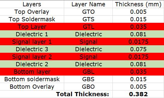
1. Layer Stackup Design
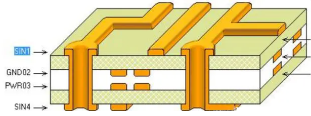
- Structural Selection: Adopt the standard 4-layer structure of “Signal Layer – Ground Plane – Power Plane – Signal Layer” to minimize crosstalk between signal layers through a complete reference plane.
- Spacing Control: Strictly control the spacing between signal layers and reference planes to 0.15-0.2mm. Outer layer copper thickness ≥35μm (1oz), inner layer ≥18μm (0.5oz), with layer-to-layer alignment accuracy verified per IPC-4101 standards (≤±50μm).
- Interlayer Coupling Optimization: Short-circuit the ground plane and power plane via metallized via arrays to form a low-impedance coupling network, suppressing interlayer noise coupling.
2. Impedance Control
- Trace Width Design: Uniformly adopt 50Ω microstrip design across the board. Use PCB manufacturer impedance calculators (e.g., Polar SI9000) to back-calculate trace width with error ≤±5%.
- Routing Standards: Prohibit 90° right-angle bends; use 135° mitered corners or circular arcs to reduce signal reflection loss (≤0.5dB@900MHz).
- Differential Signal Handling: For high-speed signals (e.g., SPI, I2C), use differential pair routing with length matching error ≤5mil and spacing ≥2× trace width. Adjust length errors via serpentine routing to reduce crosstalk to below -40dB.
3. Grounding and Power Integrity
- Ground Plane Design: Maintain a continuous, unsegmented ground plane. Short-circuit via dense metallized via arrays (spacing ≤5mm) to form low-impedance return paths, with ground impedance ≤1Ω@100MHz.
- Ground Via Optimization: Add ≥4 grounding vias near critical ICs to reduce ground impedance and suppress ground bounce noise.
- Decoupling Capacitor Layout: Implement a “0.1μF ceramic capacitor (high-frequency decoupling, distance ≤3mm) + 10μF tantalum capacitor (low-frequency energy storage)” combination at power pins. Ensure power plane impedance ≤1Ω@100MHz to avoid power noise interference with sensitive circuits.
4. Antenna Layout Optimization
- Position Planning: Place antennas on the top/bottom layer edges, away from digital signal traces (spacing ≥3× trace width) to avoid coupling interference.
- Structural Selection: Use spiral or dipole structures. Adjust gain ≥3dBi and beamwidth ≤60° via HFSS simulation to ensure coverage of target areas.
- Metal Environment Adaptation: For proximity to metal surfaces, adopt loop antenna structures. Leverage the ground plane to balance parasitic parameters, with resonant frequency stability error ≤±10MHz, compliant with ETSI 302 208 standards.
5. EMC Shielding
- Shielding Design: Install metal shields over critical circuit areas (e.g., RF modules). Integrate common-mode chokes and π-type filters (e.g., FC-L3C) at interfaces to suppress high-frequency noise.
- EMC Compliance: System-level EMC tests meet CISPR 22 Class B standards, with radiated noise ≤40dBμV/m@30MHz-1GHz and conducted emissions ≤10dBμV.
6. Signal Integrity and Thermal Management
- Signal Processing: Use serpentine routing for differential signals to match lengths. Add 22Ω series resistors to critical signals to suppress reflections and reduce overshoot (≤10%).
- Thermal Management: For high-power devices (e.g., RF power amplifiers), deploy via arrays (≥10 vias/cm?) beneath components, connecting to bottom-layer thermal pads. Validate temperature rise ≤30°C via ANSYS Icepak thermal simulation to prevent thermal failure.
7. Manufacturing Verification and Testing
Manufacturing Specifications:
- Execute laser drilling (via diameter ≥0.2mm), plating uniformity ±10%, and lamination temperature control ±2°C. Use ENIG or OSP surface finishes to ensure soldering reliability.
Testing and Tuning:
- Measure S-parameters (S11≤-15dB, S21≥-3dB) using a network analyzer to confirm antenna resonance within 860-960MHz.
- Monitor noise floor (≤-120dBm@1GHz) via spectrum analyzer to optimize filter circuits.
- Inspect pad integrity and internal defects (e.g., voids, shorts) via AOI/X-ray to ensure manufacturability.
Impedance Control Requirements for 4-Layer UHF RFID PCBs
Chip Scale Matching
- Typical input impedance of UHF RFID chips is 50±10Ω (conjugate matching value). Antenna input impedance must precisely match this value to ensure maximum power transmission efficiency.
- For example, a design case requires antenna impedance of 50Ω±5% to achieve over 95% power transfer efficiency.
Layer-to-Layer Impedance Zoning Control
- Single-ended impedance for signal layers (e.g., Top/Bottom) is typically controlled within 50-75Ω, while differential impedance requires 100±10Ω or 90±9Ω (specific values adjusted per design requirements).
- Power/ground layer spacing must be strictly controlled: errors in interlayer dielectric thickness (e.g., FR4 material) ≤5% directly impact impedance tolerance ranges.
Transmission Line Geometric Parameter Constraints
- Microstrip impedance depends on trace width (W), copper thickness (T), substrate dielectric constant (εr≈4.2-4.5), and interlayer height (H). Typical formula: Z?≈87/√εr × ln(5.98H/0.8W+T)
- Differential pair spacing must satisfy the “3W” rule (W = trace width). For high-frequency scenarios (>1GHz), upgrade to “5W” or minimum 30mil spacing; clock signals require ≥50mil isolation.
Impedance Tolerance & Verification Standards
- Manufacturing specifications must define impedance tolerance (e.g., ±10%) and verify via TDR (Time-Domain Reflectometry) or 2D/3D field solvers.
- For instance, a 4-layer HDI PCB case requires 100Ω±10% impedance, with measured values at 100.46Ω meeting design needs.
Ground & Power Layer Optimization
- Internal ground layers must form low-impedance return paths with signal layers to minimize signal reflection.
- Typical 4-layer stackup: Signal-GND-Power-Signal. Ground layer thickness ≥1oz copper foil, while power layers require decoupling capacitors (e.g., 0.1μF) to suppress noise.
Special Structural Design
- High-frequency scenarios (>3GHz) require blind/buried via designs to reduce interlayer signal loss, with controlled via diameter (e.g., 0.2mm) and spacing (≥λ/20).
- Antenna regions must avoid via interference, using solid fills or adding impedance matching networks (e.g., LC resonant circuits) for frequency tuning.
How to Reduce RF Interference in 4-Layer UHF RFID PCBs?
Layer Stackup Optimization
- Adopt “Signal-GND-Power-Signal” 4-layer stackup. Maintain 3-5mil (0.076-0.127mm) spacing between UHF antenna layer (e.g., Top) and GND plane for effective EM shielding.
- Keep power-GND spacing at 10-12mil to reduce voltage ripple and suppress high-frequency noise coupling. GND plane must remain intact without gaps to avoid radiation coupling from signal traces crossing gaps.
Impedance Matching Precision
- Design 50Ω microstrip feedlines with calculated trace widths (e.g., 3.5mil for FR4 with εr=4.2). Validate impedance continuity via TDR across 200MHz-1GHz with ±8% tolerance.
- For coplanar waveguides, set ground-trace gap ≥2× trace width to minimize edge radiation, especially for antenna feed points.
Zonal Isolation Standards
- Isolate RFID chip/antenna from digital circuits (e.g., MCU) with ≥15mm grounded copper-filled barriers. Keep high-speed digital traces (e.g., SPI clocks) ≥20mm from RFID zones to prevent harmonic coupling.
- For sensitive analog circuits (e.g., LNA input), implement 5mm-wide trench isolation in GND plane, bridged with 100pF high-frequency capacitors to balance shielding and signal integrity.
Grounding System Optimization
- Implement star-hybrid grounding: RFID chip GND pins connect directly to GND plane via ≥12mil vias (no shared vias with digital ground). Single-point connect power/digital ground at PCB edge with large copper area to minimize ground impedance. Avoid 90° cuts in GND plane; use 45° chamfers or arcs to reduce skin-effect losses at high frequencies.
Decoupling Capacitor Placement
- Use “0.1μF ceramic + 100pF” parallel decoupling at RFID VCC pins, with 0.1μF caps ≤1.5mm from pins (via-in-pad technology) and 100pF caps directly under chip GND.
- Add π-filter (10nH ferrite inductor + 100pF/10μF caps) at power entry, using low-loss inductors (e.g., TDK VLF series) to suppress >100MHz noise.
Shielding & Material Selection
- Cover sensitive areas (antenna/chip) with 0.5oz copper shielding foil, bonded 360° to GND via conductive tape to form continuous Faraday cages.
- Limit shielding window size to λ/10 (≈30mm) to prevent signal leakage. Use low-loss FR4 (tanδ≤0.012@1GHz) or Rogers RO4350B (εr=3.66, tanδ=0.0031) to minimize signal attenuation.
Routing Precision
- Route high-speed traces with 45° bends (radius ≥3× width) to avoid 90° impedance discontinuities. Equalize differential pair lengths to ±2mil via serpentine routing to suppress common-mode noise.
- Enhance power-GND capacitance coupling with via spacing ≤5mm to form a low-impedance power plane.
Antenna Matching Tuning
- Tune UHF antenna with T/π-network using network analyzer. Optimize for |S11|≤-15dB (VSWR≤1.43) across 860-960MHz.
- Use C0G capacitors and low-ESR inductors to avoid temperature drift. Maintain ≥80mm clearance from metal objects and verify radiation efficiency >85% via HFSS simulation.
How to Balance Cost and Performance in Custom 4-Layer UHF RFID PCBs?
Material Selection and Layering
- Use Rogers RO4350B (loss tangent 0.0037) in high-frequency regions (antennas, feedlines) and FR4 (loss tangent 0.015) in non-critical areas, reducing material costs by 30-50% while ensuring signal integrity.
- Select copper thickness based on needs: 1oz (35μm) suffices for UHF band (860MHz-960MHz) current requirements; thicken to 2oz (70μm) locally for high-current paths to avoid full-board cost increases.
Stack-up and Impedance Control
- Standard 4-layer structure: L1 signal layer – L2 ground layer – L3 power layer – L4 signal layer. Maintain ≤10mil (0.254mm) spacing between ground and power layers to minimize crosstalk and EMI.
- For 50Ω microstrip design on FR4, use ~3.5mil (0.089mm) trace width and ≥4mil (0.102mm) spacing, validated against PCB manufacturer’s minimum capabilities (typically 3mil/3mil).
Antenna Design and Radiation Efficiency
- Adopt folded dipole antennas (e.g., Meander lines) to reduce size by 40%, paired with T-matching networks for 50Ω impedance. Simulations show 2dB gain improvement at 920MHz and 15% extended read range.
- Implement differential feeding or coplanar waveguide (CPW) structures: CPW exhibits ~0.3dB/10cm loss on FR4, outperforming microstrip’s 0.5dB/10cm to reduce feedline losses.
Manufacturing Process Optimization
- Choose trace width/spacing supporting 3mil/3mil to prevent yield drops (10% yield loss increases costs by 5-10%).
- Surface finishes: ENIG for connector areas (high reliability), OSP for large pads (cost-effective).
- Via design: Use backdrilling or buried/blind vias for density, noting ~20% cost increase for buried vias.
Testing and Reliability Verification
- Validate impedance with TDR (±10% tolerance) for critical paths.
- Measure antenna gain, radiation patterns, and read range in an anechoic chamber, optimizing against simulation results.
- Conduct reliability tests: 85℃/85% RH for high humidity, -40℃~125℃ thermal shock for long-term stability.
FAQs of 4-Layer PCB Design for UHF RFID Application
Q1: How to achieve impedance matching for UHF RFID antennas in 4-layer PCBs?
A1: UHF RFID antennas require 50Ω impedance matching via PCB microstrip/stripline design. Calculate trace width/spacing with ground layer in top/bottom signal layers to align antenna-chip impedance. Poor matching increases reflection (VSWR), reducing read range and sensitivity.
Q2: How to allocate 4-layer PCB stackup for optimal UHF RFID performance?
A2: Use “Signal-Ground-Power-Signal” or “Signal-Power-Ground-Signal” stackup. Middle layers act as shielding cavity to minimize crosstalk. Top/bottom layers host antennas/critical signals, using adjacent ground to cut losses. Keep ground plane intact to avoid broken return paths affecting high-frequency integrity.
Q3: How to solve EMI issues in 4-layer UHF RFID PCBs?
A3: Apply “3W rule” routing, add ground via arrays to reduce interlayer noise. Isolate sensitive traces (e.g., antenna feeds) from noise sources (e.g., switching regulators). Use filter caps (0.1μF+10nF parallel) to suppress power noise. Shield signals with ground copper on both sides and dense via connections to ground.
Q4: What are special trace design rules for UHF RFID PCBs?
A4: Limit trace length ≤λ/10 (λ≈34cm@868MHz) to avoid resonance. Use rounded corners, not 90° bends, to cut impedance jumps. Match differential signal length (error ≤5mil) with controlled impedance. Avoid crossing split ground planes; prefer inner-layer stripline to reduce radiation and via count for lower parasitics.
Q5: How to validate 4-layer UHF RFID PCB performance?
A5: Test impedance with TDR, measure S11/S21 via VNA for antenna efficiency. Scan EMI with near-field probes to meet EN 302 208. Verify via real-world read tests (range/success rate). Check hotspots with thermal imaging. Simulate early with ADS/HFSS to predict signal/EMI issues.