Ever wondered how LED PCB connector ensure flawless performance in demanding applications? This guide unravels design secrets, durability hacks, and manufacturer selection strategies for gapless signal transmission and rock-solid connections.
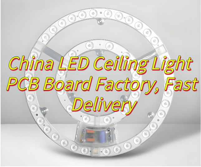
EBest Circuit (Best Technology) excels as a LED PCB board with connector manufacturer by delivering industry-leading speed and reliability. Our 24-hour rapid prototyping service and fully automated SMT production lines enable same-day sample shipments and fast mass production. With a vertically integrated facility and stable electronic component supply chain, we eliminate material shortages while maintaining consistent quality across 12 inspection checkpoints. We keep extensive inventories of common connectors (3-pin, 4-pin gapless, RGB flex) to support urgent orders. Our engineering team provides 1-hour response times for technical queries and implements design changes within 4 working hours. All products undergo rigorous environmental testing for high-temperature performance. We offer free DFM analysis and specialized gapless connector prototyping with 72-hour evaluation reports, please contact us today for good price: sales@bestpcbs.com.
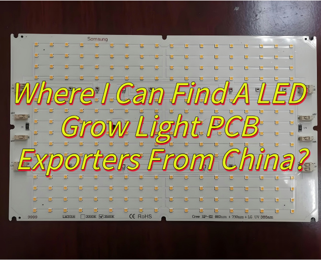
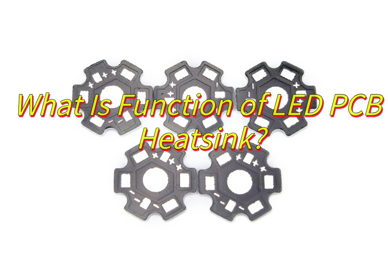
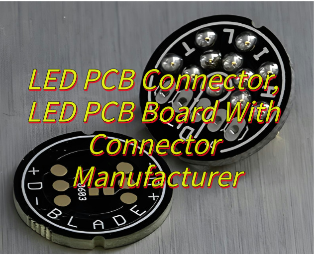
What Is LED PCB Connector?
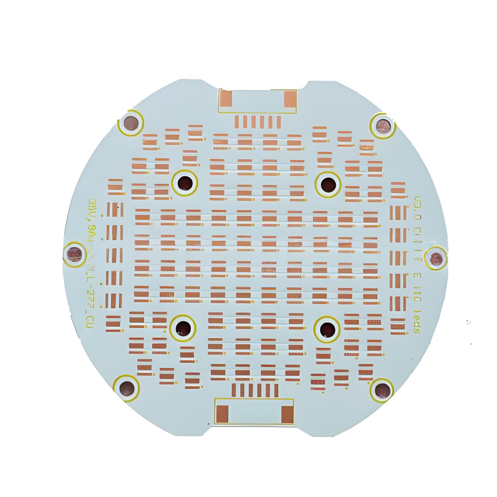
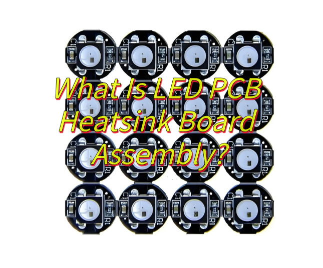
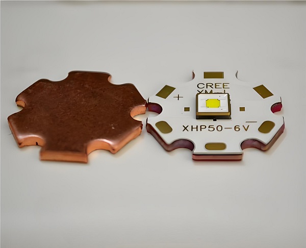
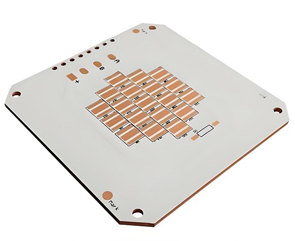
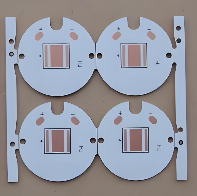
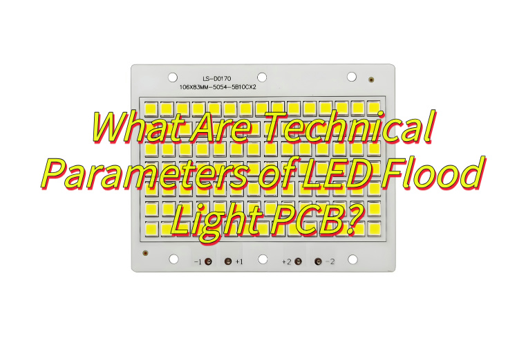
A LED PCB connector is a specialized electrical component that forms the physical and electrical interface between LED modules and printed circuit boards. These LED PCB connectors facilitate secure power transmission while allowing for modular assembly and maintenance in lighting systems. Modern LED PCB connectors typically feature corrosion resistant contacts arranged in standardized configurations to ensure compatibility across different lighting applications. The design of an LED PCB connector often incorporates locking mechanisms to prevent accidental disconnection in high vibration environments. Engineers select LED PCB connectors based on current rating requirements, with common variants supporting between 1A to 5A per contact pin. High quality LED PCB connectors maintain stable conductivity even when exposed to temperature fluctuations common in LED operation. Proper implementation of LED PCB connectors significantly impacts the longevity and performance of lighting installations across residential, commercial and industrial settings.
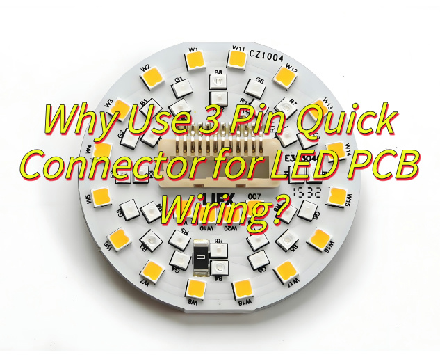
Why Use 3 Pin Quick Connector for LED PCB Wiring?
Here are the practical reasons for using 3 pin quick connectors in LED PCB wiring:
- Enhanced Electrical Safety: The 3 pin LED PCB connector provides dedicated grounding alongside power connections, reducing electrical interference and improving system safety compared to 2 pin alternatives.
- Standardized Compatibility: Most LED drivers and control systems are designed for 3 pin LED PCB connectors, ensuring broad interoperability across different lighting components.
- Simplified Maintenance: LED PCB connectors with quick release features allow technicians to replace individual LED modules without disassembling entire lighting fixtures.
- Improved Signal Integrity: In smart lighting systems, the third pin in LED PCB connectors carries control signals separately from power lines, preventing data corruption.
- Stable Mechanical Connection: Quality LED PCB connectors feature locking mechanisms that withstand vibrations in automotive or industrial applications better than basic wire connections.
- Efficient Thermal Management: The spaced pin configuration in LED PCB connectors helps distribute heat generation across multiple contact points rather than concentrating it at two terminals.
- Future Proof Design: The 3 pin LED PCB connector accommodates potential upgrades to dimmable or addressable LED systems without requiring complete rewiring.
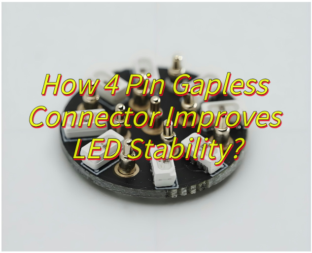
How 4 Pin Gapless Connector Improves LED Stability?
This is how 4 pin gapless connector improves LED stability:
- Contact Point Optimization: The 4-pin design enhances contact area to minimize electrical resistance, ensuring stable current delivery through the LED PCB Connector. By increasing the physical interface between pins and sockets, this configuration reduces energy loss as heat, which is critical for maintaining consistent LED brightness. A larger contact surface also distributes current more evenly, preventing localized overheating that could degrade solder joints or LED chips over time.
- Signal Integrity: The gapless structure minimizes electromagnetic interference (EMI) and cross-talk, allowing the LED PCB Connector to preserve signal clarity. This is particularly vital for addressable LED systems, where precise data transmission controls individual diode behavior. By eliminating air gaps that could act as dielectric insulators, the connector reduces impedance mismatches, ensuring commands for color changes or dimming reach their targets without distortion.
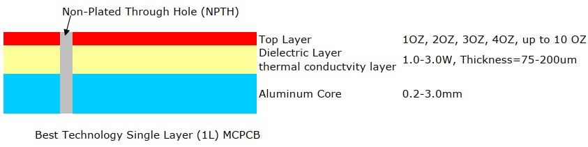
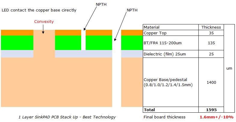
- Thermal Management: Lower contact resistance directly reduces heat generation at the junction of the LED PCB Connector. Excessive heat accelerates LED lumen depreciation and shifts color temperatures, but the 4-pin design’s efficient current pathways mitigate this risk. Additionally, some connectors incorporate thermal vias or metal-core PCBs to dissipate heat proactively, extending the operational lifespan of both the connector and the LED array.
- Mechanical Stability: The rigid housing of the 4-pin connector resists vibration and thermal expansion, maintaining reliable engagement with the LED PCB Connector. In automotive or outdoor lighting applications, mechanical stress from shocks or temperature fluctuations can loosen traditional connectors. The gapless design’s snug fit and latching mechanisms prevent micro-disconnections, ensuring uninterrupted power and signal transmission.
- Compatibility and Installation: Standardized pin spacing and polarity markers on the LED PCB Connector simplify integration across diverse PCB layouts. Manufacturers can pre-assemble connectors during PCB population, reducing soldering steps and human error risks. The modular design also supports daisy-chaining or parallel configurations, allowing flexible system scaling without redesigning the entire circuit board.
- Long-Term Reliability: By minimizing contact wear through gold-plated or nickel-coated pins, the LED PCB Connector resists oxidation and fretting corrosion. This is especially important in high-humidity environments where tarnishing could degrade performance. The 4-pin gapless architecture’s durability reduces maintenance cycles, as connectors retain their functional integrity even after thousands of mating cycles.
Can RGB LED PCB Flex Connectors Prevent Signal Loss?
Yes, RGB LED PCB flex connectors can effectively mitigate signal loss through a combination of mechanical, electrical, and material innovations. Below is an optimized explanation of their signal preservation capabilities:
- Multi-Point Contact Geometry: These connectors use staggered or dual-contact pin arrangements to create redundant electrical pathways. This design compensates for micro-movements from bending or vibration, ensuring continuous signal transmission. For example, in automotive lighting systems, this redundancy prevents color flickering during dynamic driving conditions.
- Differential Pair Routing: Advanced models integrate twisted-pair or coaxial-inspired structures within the flexible substrate to minimize inductive noise. By closely pairing data and return signals, electromagnetic interference (EMI) from adjacent power lines or wireless modules is suppressed, preserving pulse-width modulation (PWM) signal accuracy for precise RGB control.
- High-Flex Conductor Alloys: The use of beryllium copper or phosphor bronze alloys in connector pins ensures millions of flex cycles without deformation. This resistance to work hardening prevents incremental contact resistance increases, a common failure mode in consumer electronics like gaming peripherals.
- Thermal Expansion Compensation: Flex connectors often incorporate polymer fillers with matched coefficients of thermal expansion (CTE) to the PCB laminate. This prevents solder joint stress during temperature fluctuations, a critical factor in outdoor digital signage applications.
- Impedance-Controlled Traces: Manufacturers engineer specific dielectric constants into the flexible insulation to maintain consistent characteristic impedance (typically 50Ω or 100Ω). This matching prevents signal reflections that cause data errors in high-speed protocols like DMX512 or SPI, ensuring synchronized color transitions across extended LED arrays.
- Moisture-Resistant Coatings: Parylene or conformal coatings on connector surfaces repel humidity and conductive contaminants. In marine or industrial environments, this barrier prevents corrosion-induced resistive faults, maintaining signal integrity within operational thresholds.
How to Evaluate A LED PCB Board with Connector Manufacturer?
Below are how to evaluate a LED PCB board with connector manufacturer:
- Review Design and Engineering Capabilities: Assess whether the manufacturer can handle complex LED PCB layouts, including thermal management for high-power LEDs and signal integrity for addressable strips. Inquire about their experience with connector integration, such as ensuring gapless contact designs or compatibility with flexible PCB materials. A strong supplier should demonstrate proficiency in tools like Altium or Eagle for PCB design and simulation software for thermal analysis.
- Examine Quality Control Processes: Request details on their testing protocols, including automated optical inspection (AOI) for solder joints, in-circuit testing (ICT) for electrical continuity, and burn-in tests for LED longevity. Verify if they adhere to industry standards such as IPC-A-610 for PCB assembly and ISO 9001 for quality management. Ask for sample test reports to evaluate consistency in connector pin alignment and LED luminance uniformity.
- Evaluate Material Sourcing and Traceability: A reliable manufacturer should disclose their supply chain for copper-clad laminates, LED components, and connector materials. Inquire about certifications like UL for flame retardancy or RoHS compliance for lead-free soldering. Traceability systems that track batch numbers for raw materials can help identify root causes of defects, such as LED degradation or connector oxidation.
- Assess Production Flexibility and Scalability: Determine if the manufacturer supports both prototype runs and mass production. For example, ask about their minimum order quantity (MOQ) for LED PCBs with custom connector pin counts and their lead times for reordering. Flexible suppliers often offer quick-turn PCB services and can adjust production lines for mixed models, such as combining rigid and flexible PCB sections in a single panel.
- Analyze Cost Structure and Value Engineering: Compare quotes beyond unit pricing by evaluating value-added services, such as conformal coating for moisture resistance or connector pre-tinning to reduce assembly time. A transparent supplier will itemize costs for materials, labor, and testing while suggesting design tweaks—like optimizing trace widths for lower resistance—to reduce overall expenses without compromising performance.
- Check Certifications and Compliance: Ensure the manufacturer holds relevant certifications for safety and environmental standards, such as UL 8750 for LED lighting or REACH compliance for chemical restrictions. For automotive or medical applications, verify their capability to meet AEC-Q102 stress tests or ISO 13485 medical device standards, which may impact connector durability and LED reliability.
- Request Customer References and Case Studies: Ask for references from clients in similar industries, such as automotive lighting or consumer electronics, to gauge real-world performance. Case studies should detail how the manufacturer resolved challenges, like reducing signal loss in long LED strips or improving connector mating cycles in high-vibration environments.
- Audit Post-Sales Support and Warranty: Clarify their warranty terms for LED PCB failures, such as lumen maintenance beyond 10,000 hours or connector contact resistance drift. Inquire about failure analysis services, including cross-sectioning to inspect solder joints or X-ray imaging for hidden connector defects. A responsive supplier will offer technical support within 24 hours and stock spare parts for urgent replacements.

How to Verify Connector Durability for LED PCB Board with Connector?
Below are verification methods:
- Thermal Cycling Tests: Subject connectors to rapid temperature shifts (e.g., -40°C to 125°C) to simulate extreme environments. Monitor contact resistance and housing integrity over 500+ cycles to detect solder joint cracking or material embrittlement, common failure modes in automotive or outdoor lighting.
- Mechanical Vibration Testing: Use shaker tables to apply sinusoidal or random vibration profiles (e.g., 20–2000 Hz) mimicking transportation or industrial equipment use. Inspect for pin loosening, housing fractures, or signal interruptions using in-situ resistance monitoring.
- Humidity and Corrosion Resistance: Expose connectors to 85°C/85% relative humidity (RH) for 1000+ hours to accelerate oxidation. Measure insulation resistance and visualize contact surfaces with scanning electron microscopy (SEM) to assess tin whisker growth or plating degradation.
- Insertion/Withdrawal Cycle Testing: Automate mating cycles (e.g., 500–1000 insertions) to evaluate wear on gold-plated or nickel-underplated contacts. Track increasing contact resistance and check for plating delamination using cross-sectional analysis.
- Current Carrying Capacity Validation: Operate connectors at 120–150% of rated current while monitoring temperature rise via infrared thermography. Ensure compliance with UL i/i-ratio standards to prevent thermal runaway in high-power LED applications.
- Flexural Endurance for Flex PCB Variants: For flexible PCB connectors, perform dynamic bending tests (e.g., 10mm radius, 10,000 cycles) while measuring signal integrity. Assess conductor cracking via electrical impedance tomography (EIT).
- Material Compatibility Analysis: Conduct Fourier-transform infrared spectroscopy (FTIR) on polymer components to detect outgassing or chemical degradation when exposed to LED epoxies or solder flux residues.
- Industry Standard Compliance: Verify adherence to IPC-9592 for connector performance in harsh environments and AEC-Q102 for automotive LED applications. Third-party certification bodies often provide accelerated stress test protocols.
What Causes Wire-to-PCB Connector Failures in High-Temperature Environments?
Below are causes wire-to-PCB connector failures in high temperature environments:
- Material Degradation: Polymer-based connector housings or insulation layers may soften, deform, or embrittle at elevated temperatures. For example, PVC or LCP materials commonly used in connectors can lose mechanical integrity above their glass transition temperature (Tg), leading to misalignment of contacts or compromised sealing against contaminants. Similarly, metal alloys in pins or terminals may undergo annealing, reducing spring force and causing intermittent connections.
- Thermal Expansion Mismatch: Dissimilar coefficients of thermal expansion (CTE) between connector components (e.g., brass terminals vs. FR-4 PCB laminate) induce mechanical stress during temperature cycling. This mismatch can warp the connector interface, creating micro-gaps that increase contact resistance or fracture solder joints. Over time, this leads to erratic signal transmission or open circuits in LED arrays or power supplies.
- Oxidation and Corrosion: Elevated temperatures accelerate oxidation of metal surfaces, particularly at contact points. Even tin- or gold-plated terminals can develop insulating oxide layers that increase impedance, causing voltage drops or flickering in LED systems. Corrosion byproducts may also infiltrate connector interfaces, exacerbating wear during mating cycles.
- Lubricant Breakdown: Many connectors use greases or films to reduce insertion force and prevent fretting. High temperatures can volatilize or carbonize these lubricants, leaving contacts vulnerable to friction-induced wear. In automotive or aerospace applications, this degradation often manifests as increased mating resistance or particle contamination in connectors.
- Current Density and Joule Heating: At high ambient temperatures, connectors operating near their current-carrying capacity experience elevated internal heating due to Joule effects (I²R losses). This thermal runaway raises contact temperatures beyond design limits, melting solder joints or delaminating PCB traces. For instance, a connector rated for 5A at 25°C may derate to 3A at 85°C, risking failure if not de-rated appropriately.
- Solder Joint Fatigue: Thermal cycling between high ambient temperatures and operational heating causes repetitive strain on solder joints connecting connectors to PCBs. Over time, this induces cracks in the solder matrix, particularly for lead-free alloys with higher rigidity. Such failures are common in outdoor LED fixtures subjected to diurnal temperature swings.
- Insulation Resistance Reduction: Prolonged exposure to heat reduces the dielectric strength of connector insulation, increasing the risk of short circuits or arc tracking. This is critical in high-voltage applications, where compromised insulation can lead to catastrophic failure of LED drivers or power supplies.
Do Manufacturers Support Gapless LED PCB Board with Connector Prototyping?
Yes, Many manufacturers offer prototyping services for gapless LED PCB boards with integrated connectors, leveraging advanced design and production capabilities to address thermal, electrical, and mechanical challenges. These services typically include custom layout design for tight contact spacing, material selection for high-temperature stability, and iterative testing to validate signal integrity under vibration or thermal cycling. For instance, suppliers like EBest Circuit (Best Technology) provide rapid prototyping using automated optical shaping (AOS) to ensure precise alignment between LED arrays and connector pins, minimizing air gaps that could lead to arcing or signal degradation. They also incorporate simulation tools to predict thermal expansion effects on solder joints and connector housing, ensuring reliability in applications such as automotive headlights or industrial LED fixtures. Prototyping packages often include functional testing of color consistency, current leakage, and mating cycle durability, allowing engineers to refine designs before full-scale production.