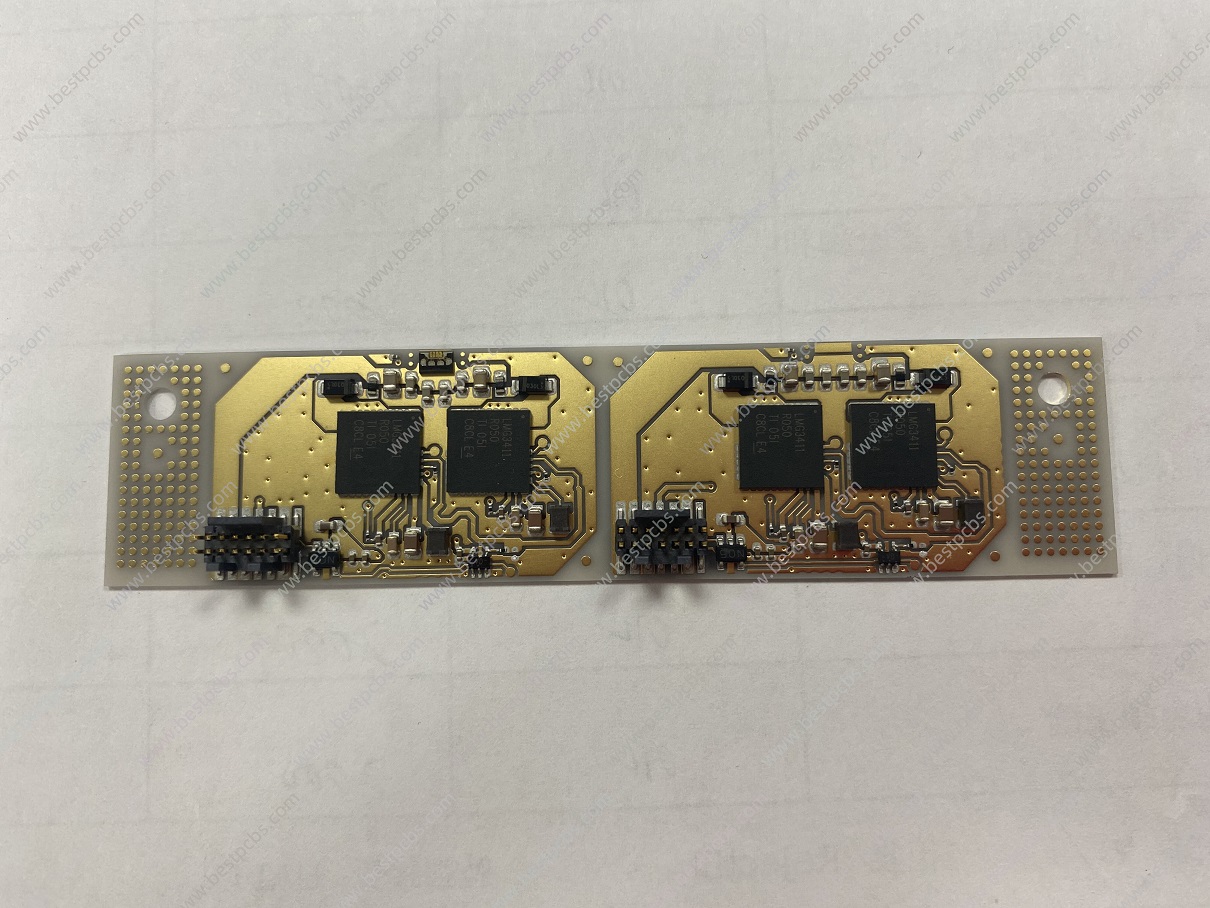
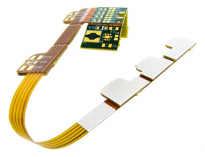
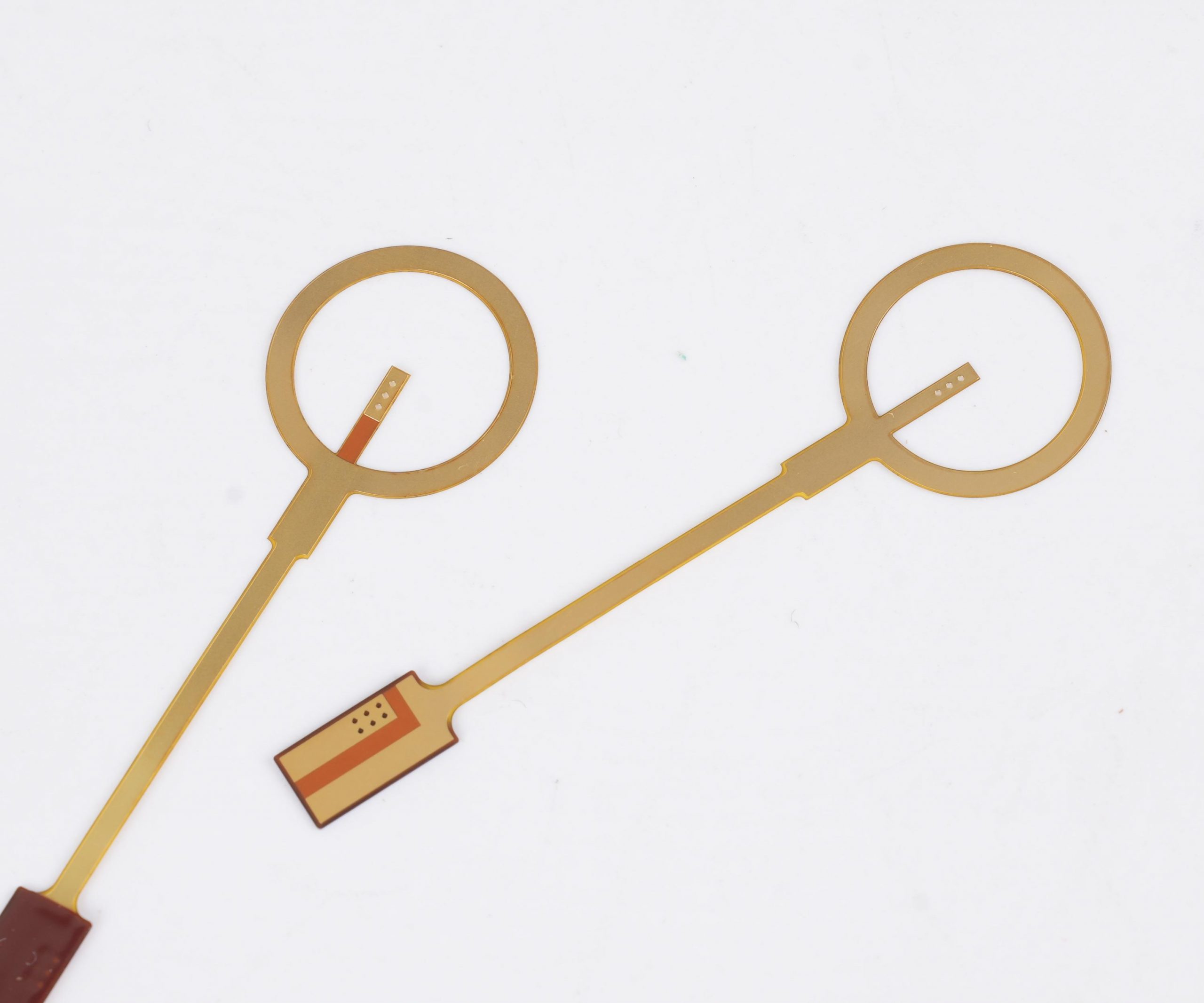
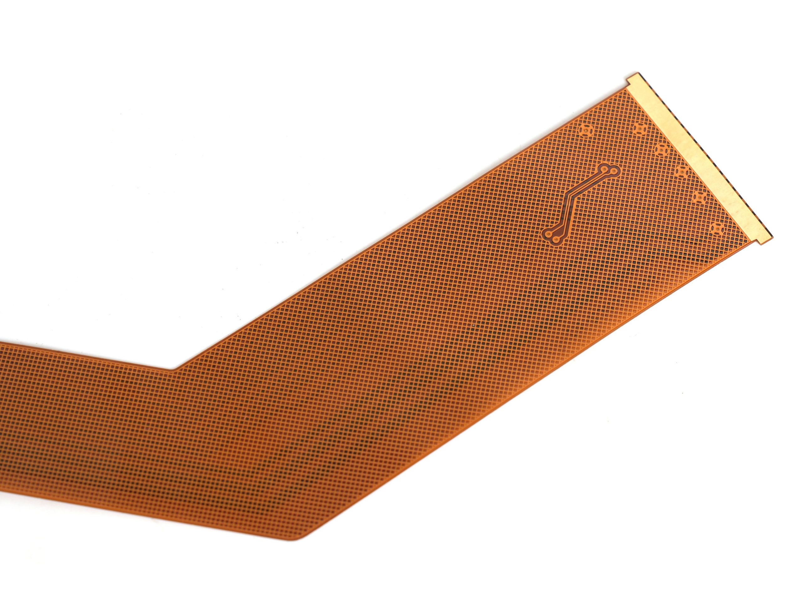
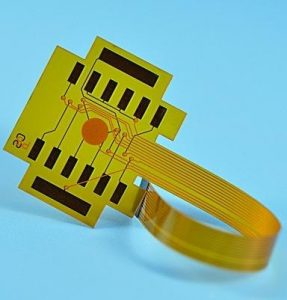
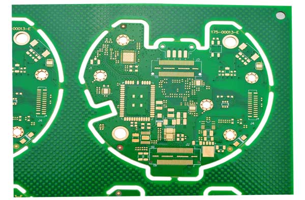
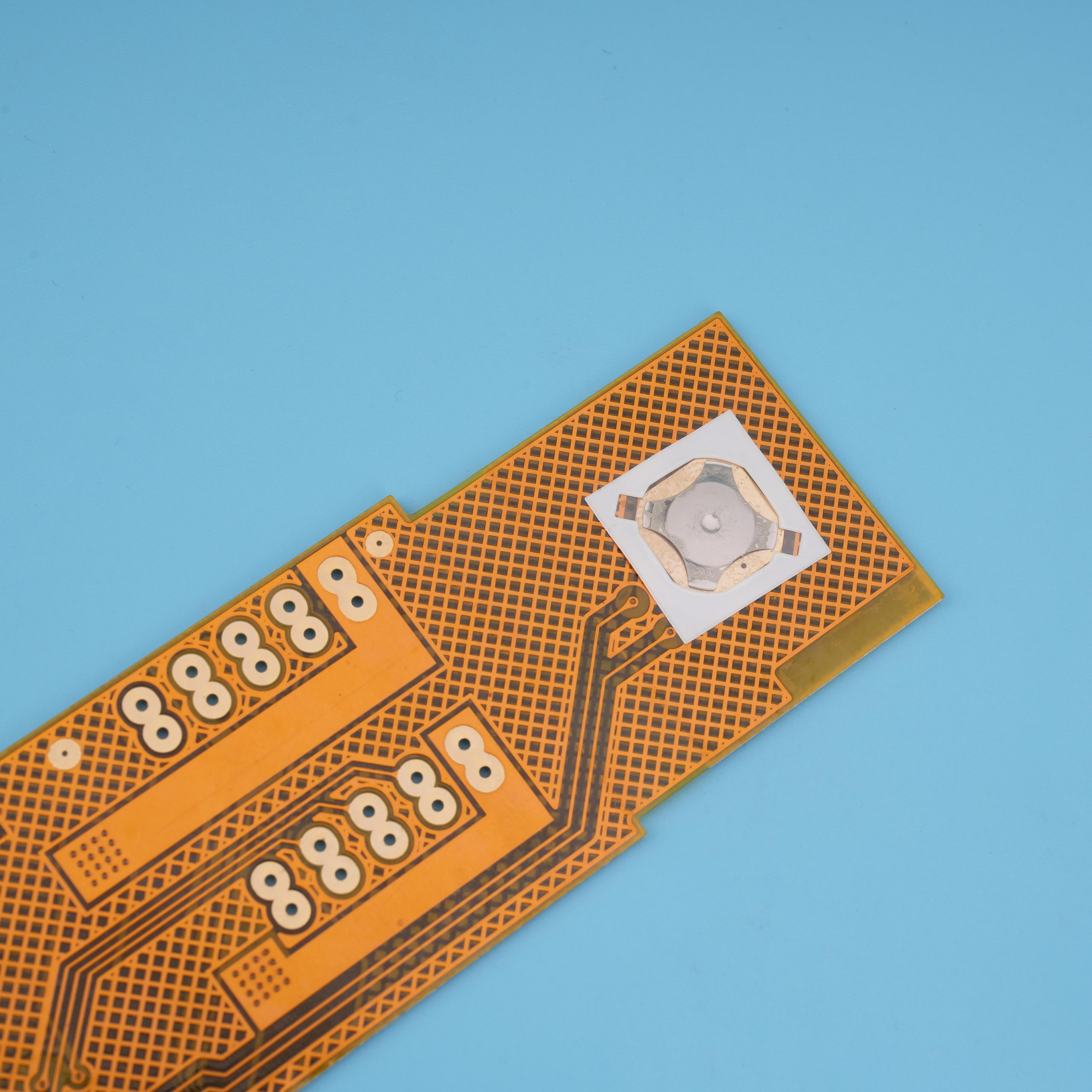
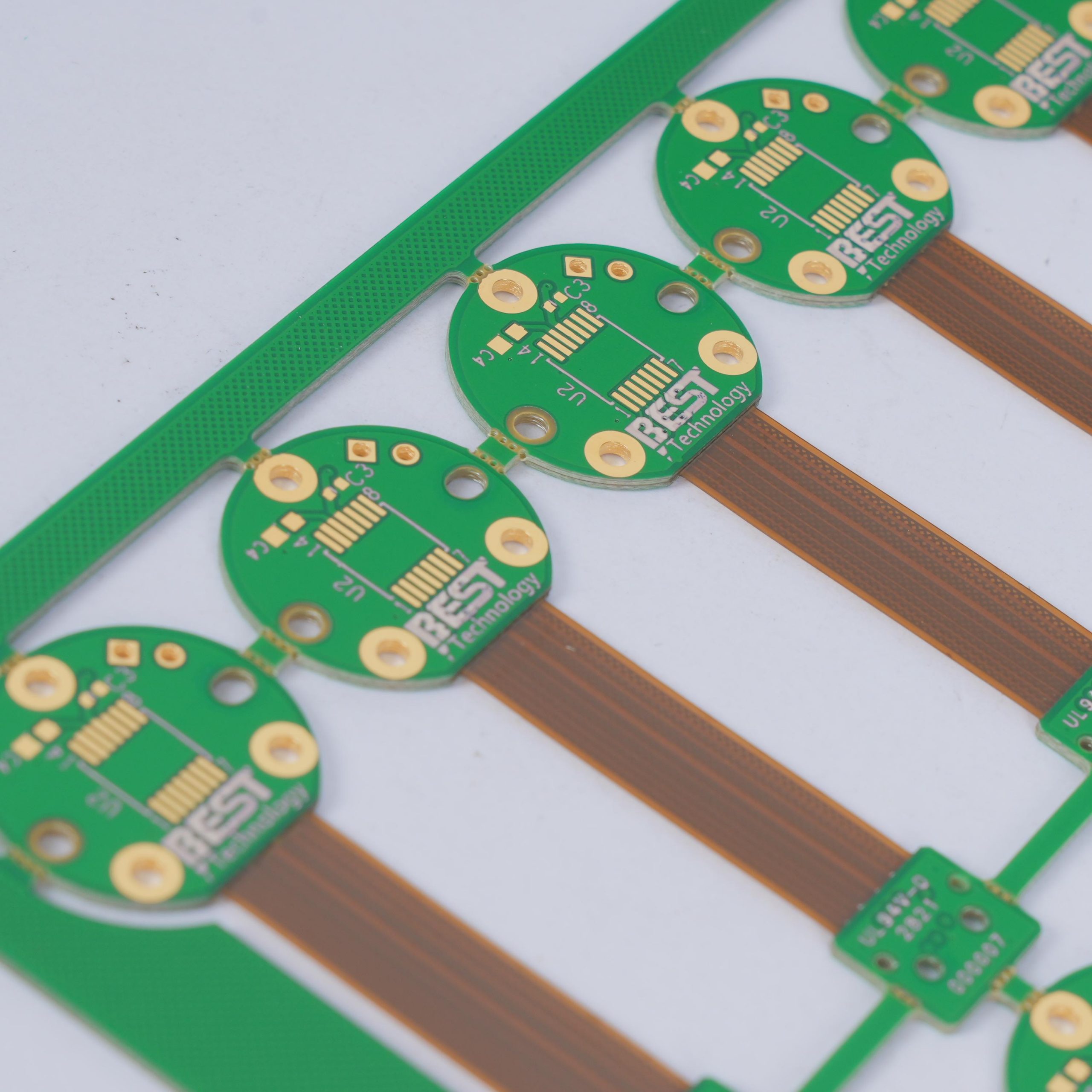
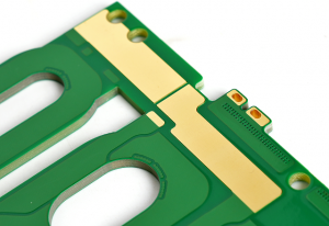
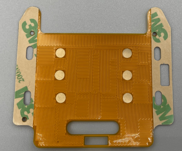
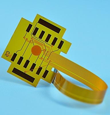
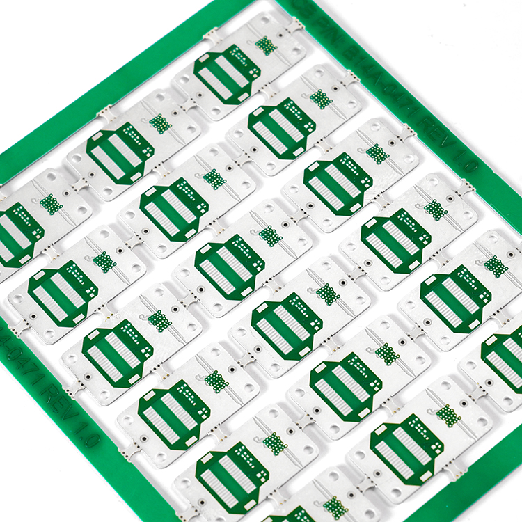
Flexible PCB is a printed circuit board made of flexible substrate, which can be bent, folded or twisted to a certain extent to meet the needs of various complex electronic device structures.
What are flexible PCBs made of?
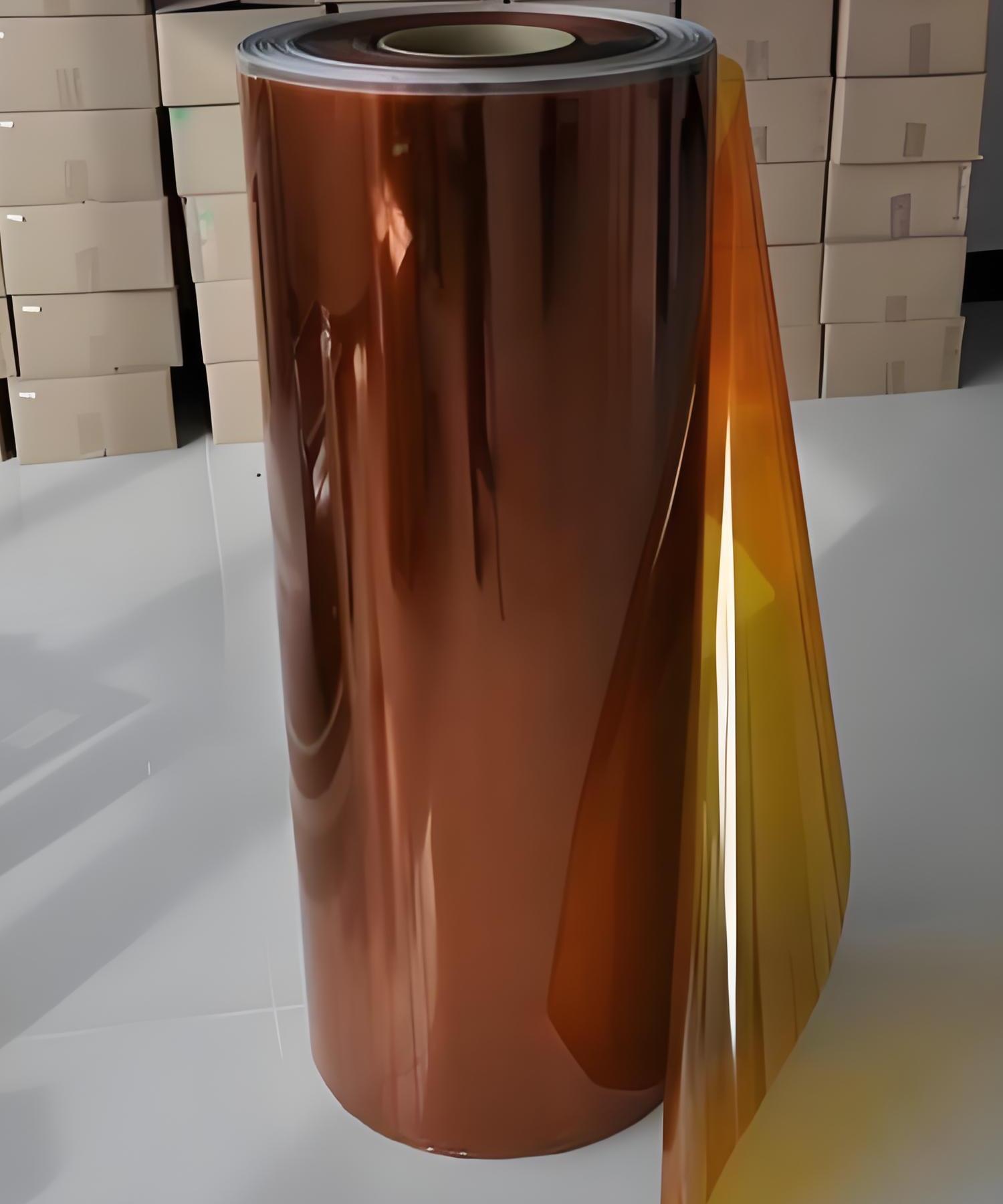
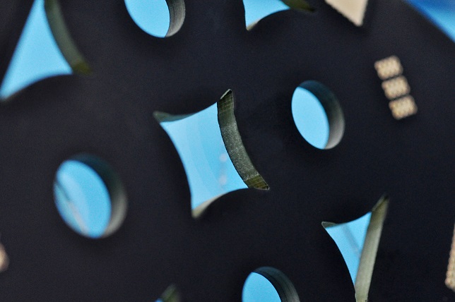
Flexible PCBs are mainly made of polyimide or polyester film. These materials have good flexibility and insulation properties, which enable flexible PCBs to maintain stable working conditions in various bending and twisting environments.
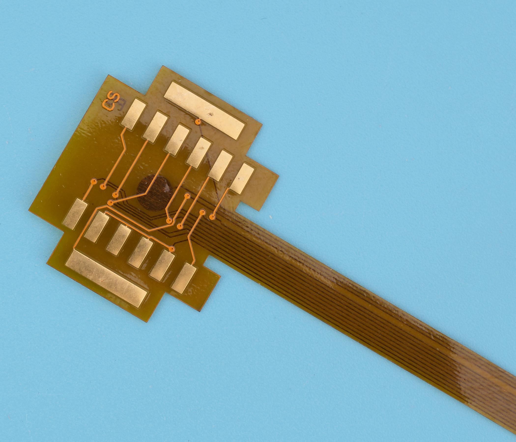
The manufacturing process of flexible PCBs includes the following main steps:
- Design phase: Use design software to create a prototype of the circuit board, determine the required lines, circuits and components, and design the shape and size of the flexible PCB according to the shape and size of the product.
- Board making phase: Print the required lines and patterns on the plastic substrate, usually using photolithography techniques such as coating photolithography and inkjet printing.
- Surface treatment and coating: Clean the circuit board and apply a protective coating to prevent chemical and mechanical wear, moisture, corrosion, etc.
- Electroplating copper: Apply electroplating copper to certain parts of the flexible PCB to thicken the line.
- Pattern chemical etching: Etch away the unnecessary parts of the circuit board and retain the required lines and components.
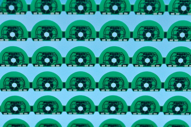
- Molding and perforation: Cut the flexible PCB into the desired shape.
What is the difference between FR4 and flex PCB?
Material composition and performance
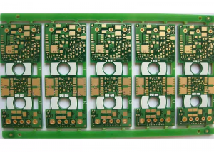
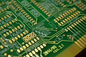
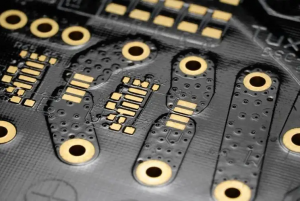
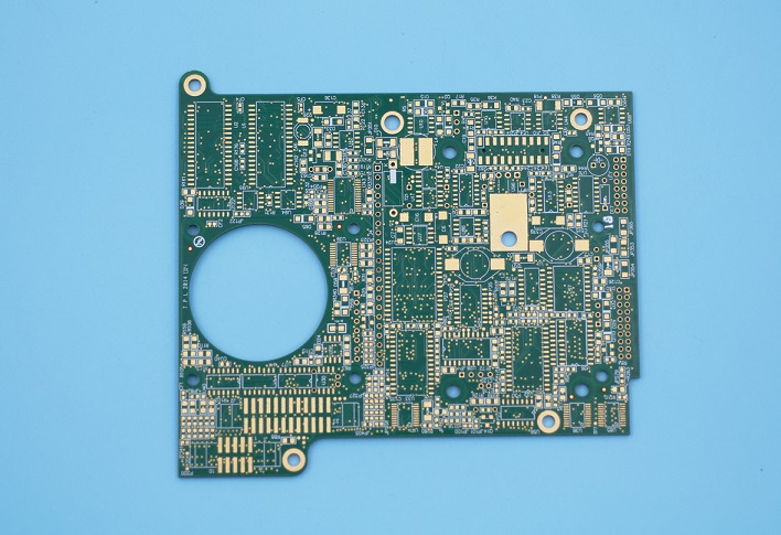
- FR4: FR4 is the most common PCB substrate, mainly composed of glass fiber and epoxy resin. It has good electrical, thermal and mechanical properties.
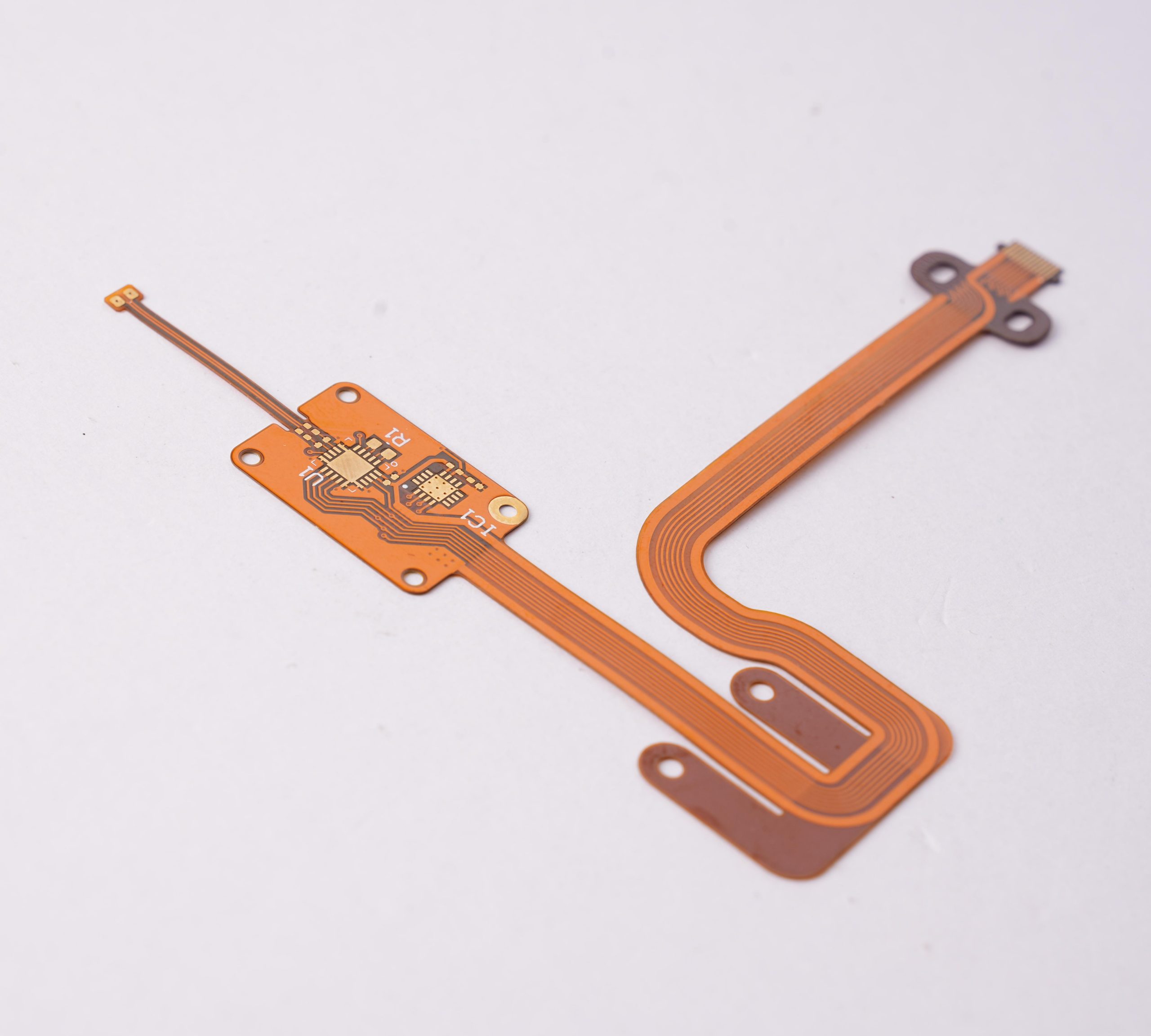
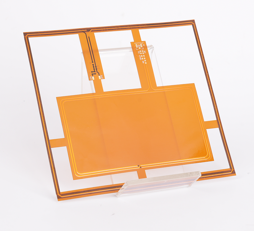
- Flexible PCB: Flexible PCB (FPC) is mainly made of materials such as polyimide (PI) and is flexible and bendable. They are often used in application scenarios that require frequent bending or limited space.
Application scenarios
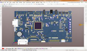
- FR4: Due to its rigidity and stability, FR4 is often used in applications that require high mechanical strength and stability, such as computer motherboards, mobile phone motherboards, etc.
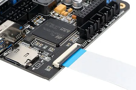
- Flexible PCB: Flexible PCB is often used in applications in car curves and corners, display screens and reverse cam screens, etc. due to its flexibility and bendability.
Manufacturing process and cost
- FR4: The manufacturing process includes drilling, etching, copper plating, etc., with moderate cost, suitable for most consumer electronic products.
- Flexible PCB: The manufacturing process is relatively complex and the cost is high, but it can meet the needs of specific applications.
In summary, FR4 and flexible PCBs have significant differences in material composition, performance and application scenarios. Choosing the right material depends on the specific application requirements.
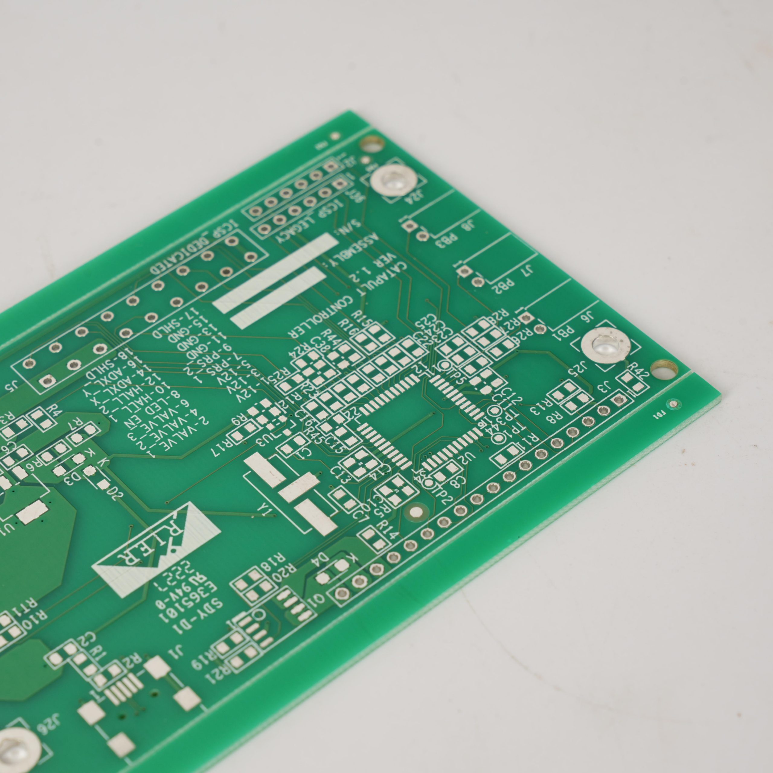
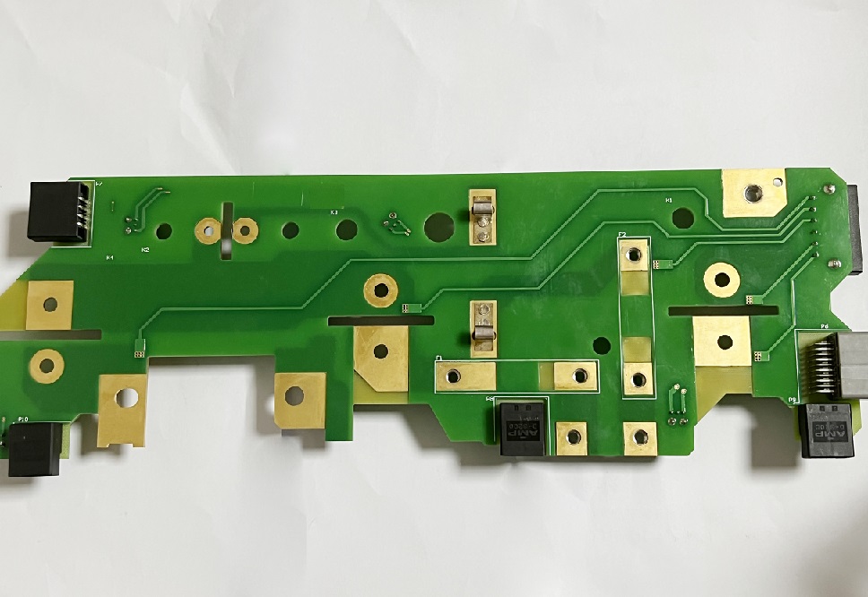
What is the difference between a rigid PCB and a flexible PCB?
The main differences between rigid PCBs and flexible PCBs include softness, load-bearing capacity, durability, heat resistance and other aspects.
- Softness: Flexible PCBs (FPCs) have good flexibility and can be easily twisted, bent and even folded, and are suitable for application scenarios that require flexible wiring. Rigid PCBs, on the other hand, are harder and cannot be bent, and are usually used in devices that require stability and high load capacity.
- Load-bearing capacity: Flexible PCBs have relatively weak current carrying capacity and are suitable for applications with smaller currents. Rigid PCBs have stronger current carrying capacity and are suitable for high-load electronic devices.
- Durability and heat resistance: Flexible PCBs can better absorb vibration and shock, have high durability and heat resistance, and can be used in extreme environments. Although rigid PCBs are thicker, they are easily damaged under the influence of high temperatures and chemicals.
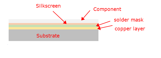
- Manufacturing process and materials: Flexible PCBs use flexible materials such as polyimide, and a cover layer process is used during the manufacturing process to protect the circuit. Rigid PCBs use thicker materials, usually made of glass-like materials, and require reinforcement.
- Application scenarios: Flexible PCBs are widely used in modern smart devices such as smartphones, tablets, and wearable devices due to their flexibility and thinness. Rigid PCBs are often used in devices that require stability and high load capacity, such as laptops and desktop computers.
In summary, there are significant differences between rigid PCBs and flexible PCBs in terms of softness, load-bearing capacity, durability, heat resistance, and application scenarios. The selection of the appropriate type of circuit board should be determined according to specific application requirements.
What is the advantage of flex PCB?
Flexible PCB (Flexible Printed Circuit, FPC for short) has the following main advantages:
- Flexibility: The main advantage of flexible PCBs is their elasticity and bending ability. They can be easily twisted, bent, and even folded, suitable for design requirements of various complex shapes.
- Reduce weight and space: Flexible PCBs not only provide greater design freedom, but also have better space utilization and weight efficiency. Due to their thin and light characteristics, flexible PCBs can greatly reduce weight and space, especially for small devices.
- Suitable for harsh environments: Flexible PCBs can be made of various corrosion-resistant materials and can withstand harsh environmental conditions.
- Better thermal management: Flexible PCBs are made of polyimide, which has excellent thermal stability and can withstand extremely high heat.
- Reduce costs: Flexible PCBs reduce assembly costs by reducing space requirements and the number of components. Since the need for wiring and connectors is reduced, testing and rework time is also reduced, improving productivity and efficiency.
In summary, flexible PCBs have significant advantages in flexibility, weight, space utilization, environmental adaptability and cost-effectiveness, making them an ideal choice for many high-tech products and applications requiring high reliability.
What are the disadvantages of flexible PCB?
The main disadvantages of flexible PCBs (FPCs) include:
- High one-time initial cost: Since flexible PCBs are designed and manufactured for special applications, the cost of circuit design, wiring and photographic plates is high.
- Difficult to change and repair: Once a flexible PCB is made, changes must start from the base map or the compiled photolithography program, so it is not easy to change. Its surface is covered with a protective film, which needs to be removed before repair and restored after repair, which is a relatively difficult task.
- Size is limited: Flexible PCB is usually manufactured by intermittent process when it is not yet popular. Therefore, it is limited by the size of production equipment and cannot be made very long or wide.
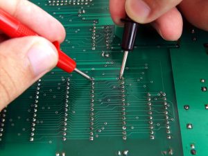
- Improper operation can easily cause damage: Improper operation by the assembly personnel can easily cause damage to the flexible circuit. Its soldering and rework require trained personnel to operate.
How thick is a flex PCB board?
The common thickness of flexible PCB board is 0.2mm. The thickening layer will be added behind the parts to be soldered. The thickness of the thickening layer is generally 0.2mm or 0.4mm12.
In addition, the thickness of flexible PCB board usually ranges from 0.1mm to 0.4mm, of which the thickness of 0.1mm to 0.4mm is called ultra-thin PCB board.
Where are flexible PCBs used?
Flexible PCB (Flexible Printed Circuit Board, FPC) is widely used in many fields, mainly including the following aspects:
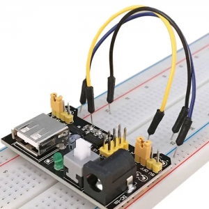
- Consumer electronics: Flexible PCB is widely used in consumer electronics such as smartphones, tablets, smart watches, etc.
- Medical equipment: In medical equipment, flexible PCB can bend and adapt to specific shapes, and is often used in electrocardiographs, blood pressure monitors, monitoring equipment and medical sensors, etc.
- Automotive electronics: Flexible PCB plays an important role in automotive electronic systems, connecting in-vehicle entertainment systems, navigation systems, dashboards, body control modules and safety systems, etc.
- Aerospace: Flexible PCB is also widely used in the aerospace field, such as satellite communications, spacecraft control, etc.
- Industrial control and automation: In the field of industrial control and automation, flexible PCB is used to connect sensors, actuators, control modules and data acquisition equipment, etc.
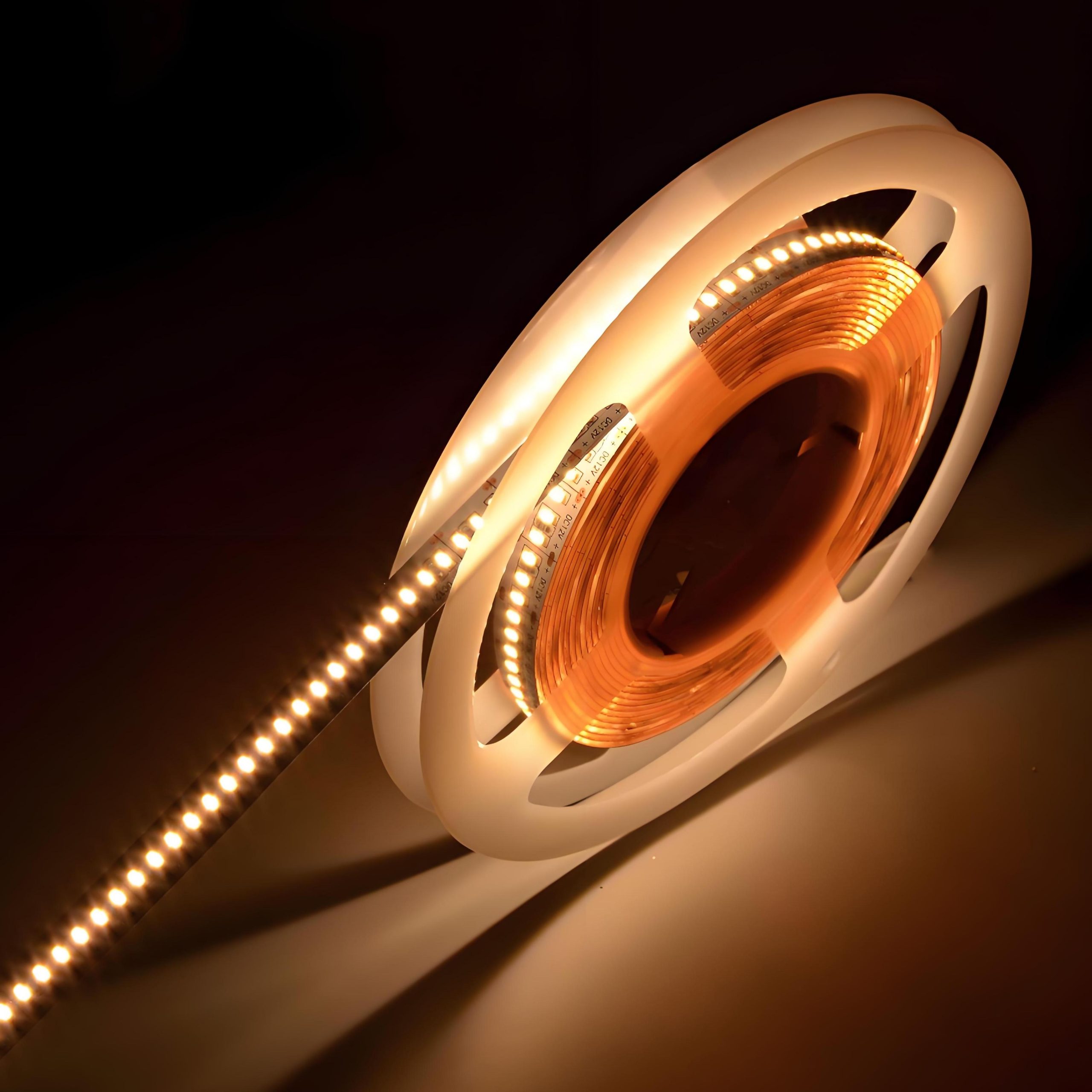
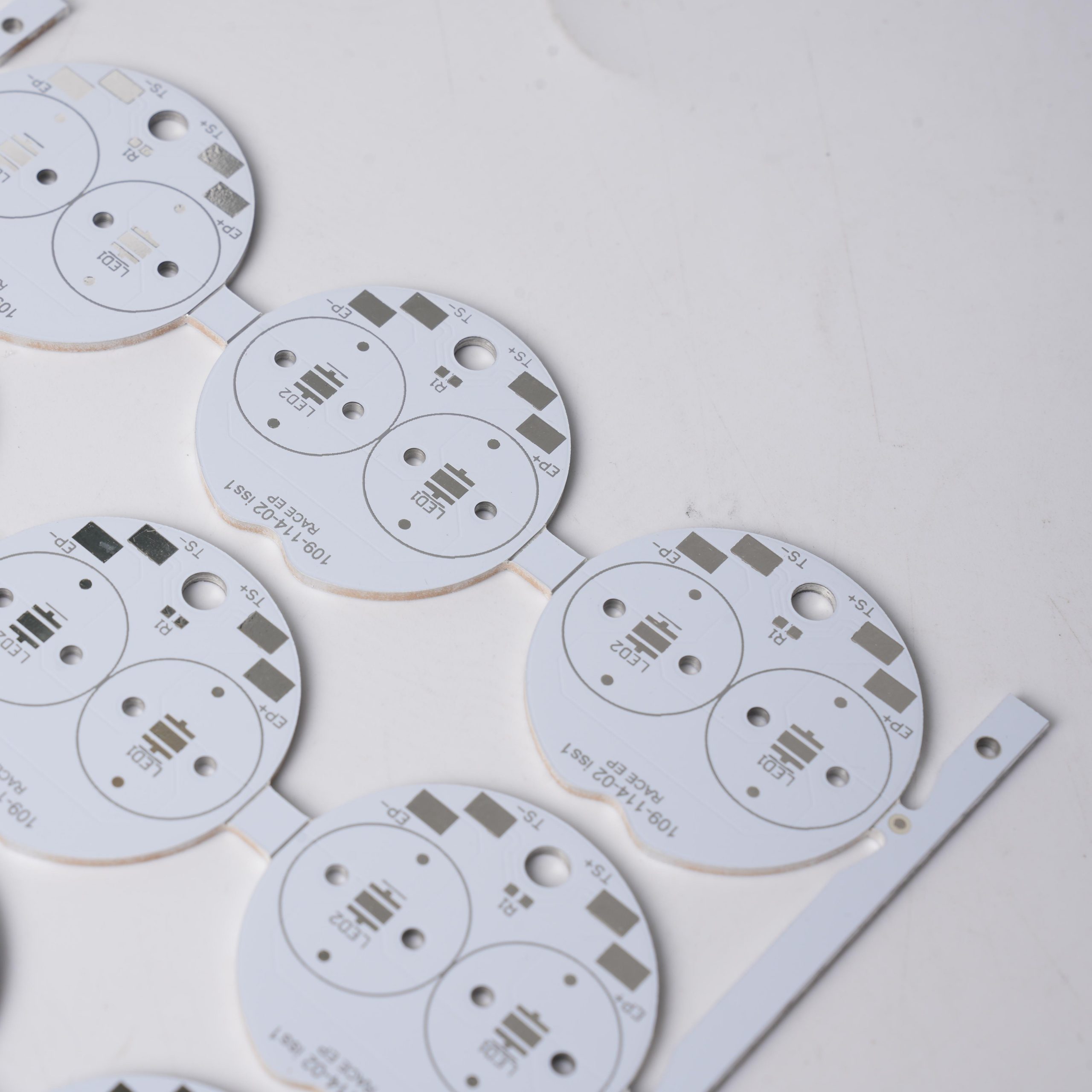
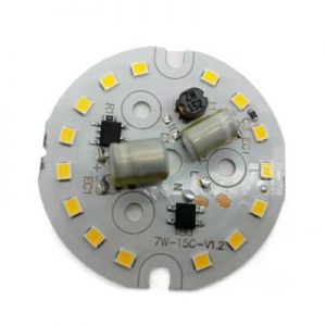
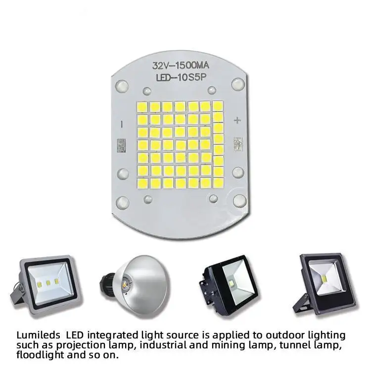
- LED lighting: Flexible PCB is also used in LED lighting products to provide connection and signal transmission functions.
In summary, the material combination of flexible PCBs gives them unique properties and a wide range of application prospects. The flexible substrate provides bendability and durability, the conductive layer ensures efficient transmission of electronic signals, and the cover layer provides protection for the entire structure. The continuous innovation and optimization of these materials will continue to promote the development of flexible PCBs.


.jpg)